|
|
市場調査レポート
商品コード
1577118
3D IC市場の2030年までの予測: コンポーネント別、タイプ別、用途別、エンドユーザー別、地域別の世界分析3D IC Market Forecasts to 2030 - Global Analysis By Component (Through Glass Via, Through-Silicon Via and Silicon Interposer), Type, Application, End User and By Geography |
||||||
|
|||||||
カスタマイズ可能
|
|||||||

| 3D IC市場の2030年までの予測: コンポーネント別、タイプ別、用途別、エンドユーザー別、地域別の世界分析 |
|
出版日: 2024年10月10日
発行: Stratistics Market Research Consulting
ページ情報: 英文 200+ Pages
納期: 2~3営業日
|

全表示
- 概要
- 図表
- 目次
Stratistics MRCによると、世界の3D IC市場は2024年に197億3,000万米ドルを占め、予測期間中にCAGR 20.9%で成長し、2030年には616億2,000万米ドルに達する見込みです。
3D IC(3次元集積回路)は、複数の半導体デバイス層を垂直に積み重ねて性能と機能を高める最先端技術です。単一平面上に配置される従来の2次元ICとは異なり、3次元ICは垂直方向の相互接続を利用するため、データ転送の高速化と信号遅延の低減が可能になります。3次元集積回路(3D IC)は、アクティブ・コンポーネントを多層に積層することで、性能の向上と実装面積の縮小を実現し、最新のエレクトロニクスに大きな利点をもたらします。
成長するデータセンターとクラウド・コンピューティング
データセンターでは、より高い性能とエネルギー効率への要求が高まっており、3D ICは、シリコンウェーハを多層に積層し、コンポーネントをより近接させることで、説得力のあるソリューションを提供します。これにより、待ち時間が短縮され、帯域幅が改善されます。さらに、3D ICは異種集積を可能にし、異なる種類のチップを1つのパッケージに組み合わせることで、機能性と電力使用量を最適化することができます。クラウド・コンピューティング・サービスが拡大するにつれ、スケーラブルで高性能なコンピューティング・ソリューションの必要性が、3D IC技術への投資と技術革新を後押ししています。
熱管理の問題
熱管理の問題は、3D集積回路の開発と性能を大きく阻害します。3Dアーキテクチャではトランジスタが垂直方向に積層されるため、部品密度が高くなり、限られたスペースでの発熱が大きくなります。不適切な熱管理は過熱、信頼性の低下、性能の低下につながるため、効果的な放熱が重要になります。従来の冷却方法では3D ICの小型化に対応できない可能性があるため、高度な熱インターフェース材料、マイクロ流体冷却システム、熱伝導技術の強化といった革新的なソリューションが必要となります。
車載アプリケーションでの採用増加
自動車が自律走行、インフォテインメント・システム、ADAS(先進運転支援システム)などの機能のために高度なエレクトロニクスへの依存度を増すにつれて、小型で高性能な部品への需要が高まっています。3D IC技術は、複数の半導体層を垂直に積み重ねることを可能にし、実装面積を縮小し、熱管理を改善します。この統合は、データ処理の高速化と電力効率の改善につながり、最新の自動車で必要とされる複雑な計算に不可欠です。
規制と標準化の課題
3D集積回路(IC)の進歩は、その普及を妨げる規制と標準化の大きな課題に直面しています。3D IC技術には、垂直方向に積層された多層の回路が組み込まれているため、さまざまなコンポーネント間の互換性と相互運用性を確保することが極めて重要です。現在のところ、設計手法、製造プロセス、試験プロトコルを規定する普遍的に受け入れられた標準は存在しないです。しかし、このような矛盾は、異なるメーカー間の協力を複雑にし、コスト増と市場投入時期の遅れにつながる可能性があります。
COVID-19の影響:
COVID-19パンデミックは3次元集積回路(IC)産業に大きな影響を与え、脆弱性と機会の両方を浮き彫りにしました。サプライチェーンの混乱により、半導体材料や部品の生産に遅れが生じ、コスト増とリードタイムの長期化につながった。メーカーが労働力不足や工場の操業停止に悩む中、コンパクトなフォームファクターでの性能向上の可能性を考慮すると、3D ICのような先進パッケージング・ソリューションに対する緊急性はより顕著になった。パンデミック時のリモートワークやデジタルサービスの急増は、高度な半導体技術に依存する高性能コンピューティングやデータセンターへの需要を加速させました。
予測期間中、シリコン貫通電極(TSV)セグメントが最大になると予想されます。
貫通電極(TSV)セグメントは、複数の半導体ダイ間の垂直相互接続を可能にすることで、予測期間中に最大となる見込みです。この革新的なアプローチにより、コンパクトな設計が可能になり、信号の移動距離が大幅に短縮されるため、性能とエネルギー効率が向上します。TSVは、より高いデータ転送速度と帯域幅を実現し、高性能コンピューティング、グラフィックス・プロセッシング、高度なモバイル機器など、高速通信を必要とするアプリケーションに不可欠です。さらに、TSVを使用したチップの3Dスタッキングによりスペースが最適化されるため、より小さなフットプリントでより多くの機能を実現できます。
予測期間中、CAGRが最も高くなると予想されるのは自動車分野です。
自動車の高度な電子機能、性能向上、小型化に対する要求が高まっているため、予測期間中、自動車分野のCAGRが最も高くなると予想されます。3D ICは、複数の回路層を垂直に積み重ねることを可能にし、スペース効率と電力管理を大幅に改善します。この技術は、ADAS(先進運転支援システム)、インフォテインメント、電気自動車(EV)管理などのアプリケーションに不可欠な、センシング、プロセッシング、通信などのさまざまな機能を単一の小型パッケージに統合することを容易にします。さらに、3D ICは、自律走行システムにおけるリアルタイムのデータ処理と意思決定に不可欠な高帯域幅と低遅延に貢献します。
最大のシェアを占める地域:
北米地域は、1チップ内でメモリと処理機能をシームレスに組み合わせることができるため、予測期間中、同市場で最大のシェアを占めると予想されます。ロジック・コンポーネントの上にメモリを直接積層することで、メーカーはコンパクトな設計を維持しながら、より高い帯域幅と密度を達成することができます。北米が半導体技術開発をリードし続ける中、メモリとロジックの統合に注力することで、技術大手と新興企業のコラボレーションが促進され、さらなる進歩が見込まれます。この進化は電子機器の性能を向上させるだけでなく、この地域を世界の半導体技術革新の最前線に位置付け、急速に進歩する技術情勢の中で競争力を維持することを確実にします。
CAGRが最も高い地域:
欧州地域は予測期間中、収益性の高い成長を維持する見込みです。安全性、環境への影響、性能について厳しい基準を設けることで、これらの規制は3D IC技術の革新がより広範な持続可能性の目標に合致することを保証します。これは消費者や業界の利害関係者の信頼を醸成するだけでなく、研究開発への投資も促進します。標準化が重視されることで、デバイス間の相互運用性が高まり、より効率的な製造プロセスへの道が開かれ、新製品の市場投入までの時間が短縮されます。欧州政府もデジタル主権を優先するため、半導体分野の現地生産と技術革新にインセンティブを与え、この地域が世界規模で競争力を維持できるようにしています。
無料のカスタマイズサービス:
本レポートをご購読のお客様には、以下の無料カスタマイズオプションのいずれかをご利用いただけます:
- 企業プロファイル
- 追加市場プレーヤーの包括的プロファイリング(3社まで)
- 主要企業のSWOT分析(3社まで)
- 地域セグメンテーション
- 顧客の関心に応じた主要国の市場推計・予測・CAGR(注:フィージビリティチェックによる)
- 競合ベンチマーキング
- 製品ポートフォリオ、地理的プレゼンス、戦略的提携に基づく主要企業のベンチマーキング
目次
第1章 エグゼクティブサマリー
第2章 序文
- 概要
- ステークホルダー
- 調査範囲
- 調査手法
- データマイニング
- データ分析
- データ検証
- 調査アプローチ
- 調査情報源
- 1次調査情報源
- 2次調査情報源
- 前提条件
第3章 市場動向分析
- 促進要因
- 抑制要因
- 機会
- 脅威
- 用途分析
- エンドユーザー分析
- 新興市場
- COVID-19の影響
第4章 ポーターのファイブフォース分析
- 供給企業の交渉力
- 買い手の交渉力
- 代替品の脅威
- 新規参入業者の脅威
- 競争企業間の敵対関係
第5章 世界の3D IC市場:コンポーネント別
- ガラス貫通ビア(TGV)
- シリコン貫通ビア(TSV)
- シリコンインターポーザ
第6章 世界の3D IC市場:タイプ別
- モノリシック 3D
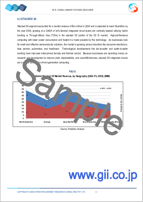
- スタック3D
第7章 世界の3D IC市場:用途別
- 航空宇宙
- イメージングとオプトエレクトロニクス
- センサー
- その他の用途
第8章 世界の3D IC市場:エンドユーザー別
- 通信
- 家電
- 自動車
- 医療機器
- その他のエンドユーザー
第9章 世界の3D IC市場:地域別
- 北米
- 米国
- カナダ
- メキシコ
- 欧州
- ドイツ
- 英国
- イタリア
- フランス
- スペイン
- その他欧州
- アジア太平洋
- 日本
- 中国
- インド
- オーストラリア
- ニュージーランド
- 韓国
- その他アジア太平洋地域
- 南米
- アルゼンチン
- ブラジル
- チリ
- その他南米
- 中東・アフリカ
- サウジアラビア
- アラブ首長国連邦
- カタール
- 南アフリカ
- その他中東とアフリカ
第10章 主な発展
- 契約、パートナーシップ、コラボレーション、合弁事業
- 買収と合併
- 新製品発売
- 事業拡大
- その他の主要戦略
第11章 企業プロファイリング
- ASE Group
- Infineon Technologies
- Intel Corporation
- Keyence Corporation
- NXP Semiconductors
- Qualcomm Incorporated
- Renesas Electronics
- Siliconware Precision Industries
- Synopsys
- United Microelectronics Corporation
List of Tables
- Table 1 Global 3D IC Market Outlook, By Region (2022-2030) ($MN)
- Table 2 Global 3D IC Market Outlook, By Component (2022-2030) ($MN)
- Table 3 Global 3D IC Market Outlook, By Through Glass Via (TGV) (2022-2030) ($MN)
- Table 4 Global 3D IC Market Outlook, By Through-Silicon Via (TSV) (2022-2030) ($MN)
- Table 5 Global 3D IC Market Outlook, By Silicon Interposer (2022-2030) ($MN)
- Table 6 Global 3D IC Market Outlook, By Type (2022-2030) ($MN)
- Table 7 Global 3D IC Market Outlook, By Monolithic 3D (2022-2030) ($MN)
- Table 8 Global 3D IC Market Outlook, By Stacked 3D (2022-2030) ($MN)
- Table 9 Global 3D IC Market Outlook, By Application (2022-2030) ($MN)
- Table 10 Global 3D IC Market Outlook, By Aerospace (2022-2030) ($MN)
- Table 11 Global 3D IC Market Outlook, By Imaging and Optoelectronics (2022-2030) ($MN)
- Table 12 Global 3D IC Market Outlook, By Sensors (2022-2030) ($MN)
- Table 13 Global 3D IC Market Outlook, By Other Applications (2022-2030) ($MN)
- Table 14 Global 3D IC Market Outlook, By End User (2022-2030) ($MN)
- Table 15 Global 3D IC Market Outlook, By Telecommunications (2022-2030) ($MN)
- Table 16 Global 3D IC Market Outlook, By Consumer Electronics (2022-2030) ($MN)
- Table 17 Global 3D IC Market Outlook, By Automotive (2022-2030) ($MN)
- Table 18 Global 3D IC Market Outlook, By Medical Devices (2022-2030) ($MN)
- Table 19 Global 3D IC Market Outlook, By Other End Users (2022-2030) ($MN)
- Table 20 North America 3D IC Market Outlook, By Country (2022-2030) ($MN)
- Table 21 North America 3D IC Market Outlook, By Component (2022-2030) ($MN)
- Table 22 North America 3D IC Market Outlook, By Through Glass Via (TGV) (2022-2030) ($MN)
- Table 23 North America 3D IC Market Outlook, By Through-Silicon Via (TSV) (2022-2030) ($MN)
- Table 24 North America 3D IC Market Outlook, By Silicon Interposer (2022-2030) ($MN)
- Table 25 North America 3D IC Market Outlook, By Type (2022-2030) ($MN)
- Table 26 North America 3D IC Market Outlook, By Monolithic 3D (2022-2030) ($MN)
- Table 27 North America 3D IC Market Outlook, By Stacked 3D (2022-2030) ($MN)
- Table 28 North America 3D IC Market Outlook, By Application (2022-2030) ($MN)
- Table 29 North America 3D IC Market Outlook, By Aerospace (2022-2030) ($MN)
- Table 30 North America 3D IC Market Outlook, By Imaging and Optoelectronics (2022-2030) ($MN)
- Table 31 North America 3D IC Market Outlook, By Sensors (2022-2030) ($MN)
- Table 32 North America 3D IC Market Outlook, By Other Applications (2022-2030) ($MN)
- Table 33 North America 3D IC Market Outlook, By End User (2022-2030) ($MN)
- Table 34 North America 3D IC Market Outlook, By Telecommunications (2022-2030) ($MN)
- Table 35 North America 3D IC Market Outlook, By Consumer Electronics (2022-2030) ($MN)
- Table 36 North America 3D IC Market Outlook, By Automotive (2022-2030) ($MN)
- Table 37 North America 3D IC Market Outlook, By Medical Devices (2022-2030) ($MN)
- Table 38 North America 3D IC Market Outlook, By Other End Users (2022-2030) ($MN)
- Table 39 Europe 3D IC Market Outlook, By Country (2022-2030) ($MN)
- Table 40 Europe 3D IC Market Outlook, By Component (2022-2030) ($MN)
- Table 41 Europe 3D IC Market Outlook, By Through Glass Via (TGV) (2022-2030) ($MN)
- Table 42 Europe 3D IC Market Outlook, By Through-Silicon Via (TSV) (2022-2030) ($MN)
- Table 43 Europe 3D IC Market Outlook, By Silicon Interposer (2022-2030) ($MN)
- Table 44 Europe 3D IC Market Outlook, By Type (2022-2030) ($MN)
- Table 45 Europe 3D IC Market Outlook, By Monolithic 3D (2022-2030) ($MN)
- Table 46 Europe 3D IC Market Outlook, By Stacked 3D (2022-2030) ($MN)
- Table 47 Europe 3D IC Market Outlook, By Application (2022-2030) ($MN)
- Table 48 Europe 3D IC Market Outlook, By Aerospace (2022-2030) ($MN)
- Table 49 Europe 3D IC Market Outlook, By Imaging and Optoelectronics (2022-2030) ($MN)
- Table 50 Europe 3D IC Market Outlook, By Sensors (2022-2030) ($MN)
- Table 51 Europe 3D IC Market Outlook, By Other Applications (2022-2030) ($MN)
- Table 52 Europe 3D IC Market Outlook, By End User (2022-2030) ($MN)
- Table 53 Europe 3D IC Market Outlook, By Telecommunications (2022-2030) ($MN)
- Table 54 Europe 3D IC Market Outlook, By Consumer Electronics (2022-2030) ($MN)
- Table 55 Europe 3D IC Market Outlook, By Automotive (2022-2030) ($MN)
- Table 56 Europe 3D IC Market Outlook, By Medical Devices (2022-2030) ($MN)
- Table 57 Europe 3D IC Market Outlook, By Other End Users (2022-2030) ($MN)
- Table 58 Asia Pacific 3D IC Market Outlook, By Country (2022-2030) ($MN)
- Table 59 Asia Pacific 3D IC Market Outlook, By Component (2022-2030) ($MN)
- Table 60 Asia Pacific 3D IC Market Outlook, By Through Glass Via (TGV) (2022-2030) ($MN)
- Table 61 Asia Pacific 3D IC Market Outlook, By Through-Silicon Via (TSV) (2022-2030) ($MN)
- Table 62 Asia Pacific 3D IC Market Outlook, By Silicon Interposer (2022-2030) ($MN)
- Table 63 Asia Pacific 3D IC Market Outlook, By Type (2022-2030) ($MN)
- Table 64 Asia Pacific 3D IC Market Outlook, By Monolithic 3D (2022-2030) ($MN)
- Table 65 Asia Pacific 3D IC Market Outlook, By Stacked 3D (2022-2030) ($MN)
- Table 66 Asia Pacific 3D IC Market Outlook, By Application (2022-2030) ($MN)
- Table 67 Asia Pacific 3D IC Market Outlook, By Aerospace (2022-2030) ($MN)
- Table 68 Asia Pacific 3D IC Market Outlook, By Imaging and Optoelectronics (2022-2030) ($MN)
- Table 69 Asia Pacific 3D IC Market Outlook, By Sensors (2022-2030) ($MN)
- Table 70 Asia Pacific 3D IC Market Outlook, By Other Applications (2022-2030) ($MN)
- Table 71 Asia Pacific 3D IC Market Outlook, By End User (2022-2030) ($MN)
- Table 72 Asia Pacific 3D IC Market Outlook, By Telecommunications (2022-2030) ($MN)
- Table 73 Asia Pacific 3D IC Market Outlook, By Consumer Electronics (2022-2030) ($MN)
- Table 74 Asia Pacific 3D IC Market Outlook, By Automotive (2022-2030) ($MN)
- Table 75 Asia Pacific 3D IC Market Outlook, By Medical Devices (2022-2030) ($MN)
- Table 76 Asia Pacific 3D IC Market Outlook, By Other End Users (2022-2030) ($MN)
- Table 77 South America 3D IC Market Outlook, By Country (2022-2030) ($MN)
- Table 78 South America 3D IC Market Outlook, By Component (2022-2030) ($MN)
- Table 79 South America 3D IC Market Outlook, By Through Glass Via (TGV) (2022-2030) ($MN)
- Table 80 South America 3D IC Market Outlook, By Through-Silicon Via (TSV) (2022-2030) ($MN)
- Table 81 South America 3D IC Market Outlook, By Silicon Interposer (2022-2030) ($MN)
- Table 82 South America 3D IC Market Outlook, By Type (2022-2030) ($MN)
- Table 83 South America 3D IC Market Outlook, By Monolithic 3D (2022-2030) ($MN)
- Table 84 South America 3D IC Market Outlook, By Stacked 3D (2022-2030) ($MN)
- Table 85 South America 3D IC Market Outlook, By Application (2022-2030) ($MN)
- Table 86 South America 3D IC Market Outlook, By Aerospace (2022-2030) ($MN)
- Table 87 South America 3D IC Market Outlook, By Imaging and Optoelectronics (2022-2030) ($MN)
- Table 88 South America 3D IC Market Outlook, By Sensors (2022-2030) ($MN)
- Table 89 South America 3D IC Market Outlook, By Other Applications (2022-2030) ($MN)
- Table 90 South America 3D IC Market Outlook, By End User (2022-2030) ($MN)
- Table 91 South America 3D IC Market Outlook, By Telecommunications (2022-2030) ($MN)
- Table 92 South America 3D IC Market Outlook, By Consumer Electronics (2022-2030) ($MN)
- Table 93 South America 3D IC Market Outlook, By Automotive (2022-2030) ($MN)
- Table 94 South America 3D IC Market Outlook, By Medical Devices (2022-2030) ($MN)
- Table 95 South America 3D IC Market Outlook, By Other End Users (2022-2030) ($MN)
- Table 96 Middle East & Africa 3D IC Market Outlook, By Country (2022-2030) ($MN)
- Table 97 Middle East & Africa 3D IC Market Outlook, By Component (2022-2030) ($MN)
- Table 98 Middle East & Africa 3D IC Market Outlook, By Through Glass Via (TGV) (2022-2030) ($MN)
- Table 99 Middle East & Africa 3D IC Market Outlook, By Through-Silicon Via (TSV) (2022-2030) ($MN)
- Table 100 Middle East & Africa 3D IC Market Outlook, By Silicon Interposer (2022-2030) ($MN)
- Table 101 Middle East & Africa 3D IC Market Outlook, By Type (2022-2030) ($MN)
- Table 102 Middle East & Africa 3D IC Market Outlook, By Monolithic 3D (2022-2030) ($MN)
- Table 103 Middle East & Africa 3D IC Market Outlook, By Stacked 3D (2022-2030) ($MN)
- Table 104 Middle East & Africa 3D IC Market Outlook, By Application (2022-2030) ($MN)
- Table 105 Middle East & Africa 3D IC Market Outlook, By Aerospace (2022-2030) ($MN)
- Table 106 Middle East & Africa 3D IC Market Outlook, By Imaging and Optoelectronics (2022-2030) ($MN)
- Table 107 Middle East & Africa 3D IC Market Outlook, By Sensors (2022-2030) ($MN)
- Table 108 Middle East & Africa 3D IC Market Outlook, By Other Applications (2022-2030) ($MN)
- Table 109 Middle East & Africa 3D IC Market Outlook, By End User (2022-2030) ($MN)
- Table 110 Middle East & Africa 3D IC Market Outlook, By Telecommunications (2022-2030) ($MN)
- Table 111 Middle East & Africa 3D IC Market Outlook, By Consumer Electronics (2022-2030) ($MN)
- Table 112 Middle East & Africa 3D IC Market Outlook, By Automotive (2022-2030) ($MN)
- Table 113 Middle East & Africa 3D IC Market Outlook, By Medical Devices (2022-2030) ($MN)
- Table 114 Middle East & Africa 3D IC Market Outlook, By Other End Users (2022-2030) ($MN)
According to Stratistics MRC, the Global 3D IC Market is accounted for $19.73 billion in 2024 and is expected to reach $61.62 billion by 2030 growing at a CAGR of 20.9% during the forecast period. A 3D IC, or three-dimensional integrated circuit, is a cutting-edge technology that stacks multiple layers of semiconductor devices vertically to enhance performance and functionality. Unlike traditional 2D ICs, which are laid out on a single plane, 3D ICs utilize vertical interconnections, enabling faster data transfer and reduced signal delay. Three-dimensional integrated circuits (3D ICs) offer significant advantages in modern electronics by stacking multiple layers of active components, leading to enhanced performance and reduced footprint.
Market Dynamics:
Driver:
Growing data centers and cloud computing
As the demand for higher performance and energy efficiency escalates in data centers, 3D ICs provide a compelling solution by stacking multiple layers of silicon wafers, enabling closer proximity of components. This reduces latency and improves bandwidth, crucial for handling massive data loads efficiently. Additionally, 3D ICs allow for heterogeneous integration, where different types of chips can be combined in a single package, optimizing functionality and power usage. As cloud computing services expand, the need for scalable, high-performance computing solutions drives investment and innovation in 3D IC technology.
Restraint:
Thermal management issues
Thermal management issues significantly hinder the development and performance of 3D integrated circuits. As transistors are stacked vertically in 3D architectures, the density of components increases, leading to higher heat generation in a confined space. Effective heat dissipation becomes critical, as inadequate thermal management can result in overheating, reduced reliability and lower performance. Traditional cooling methods may not be sufficient for the compactness of 3D ICs, necessitating innovative solutions such as advanced thermal interface materials, microfluidic cooling systems, or enhanced thermal conduction techniques.
Opportunity:
Rising adoption in automotive applications
As vehicles become increasingly reliant on advanced electronics for features like autonomous driving, infotainment systems, and advanced driver-assistance systems (ADAS), the demand for compact and high-performance components grows. 3D IC technology allows for vertical stacking of multiple semiconductor layers, reducing the footprint and improving thermal management. This integration leads to faster data processing and improved power efficiency, essential for the complex computations required in modern vehicles.
Threat:
Regulatory and standardization challenges
The advancement of 3D integrated circuits (ICs) faces significant regulatory and standardization challenges that hinder their widespread adoption. As 3D IC technology incorporates multiple layers of circuitry stacked vertically, ensuring compatibility and interoperability among various components is crucial. Currently, there is a lack of universally accepted standards governing design methodologies, manufacturing processes, and testing protocols. However, this inconsistency complicates collaboration among different manufacturers and can lead to increased costs and time-to-market delays.
Covid-19 Impact:
The COVID-19 pandemic significantly impacted the 3D integrated circuit (IC) industry, highlighting both vulnerabilities and opportunities. Supply chain disruptions caused delays in the production of semiconductor materials and components, leading to increased costs and longer lead times. As manufacturers grappled with labor shortages and factory shutdowns, the urgency for advanced packaging solutions like 3D ICs became more pronounced, given their potential for enhanced performance in compact form factors. The surge in remote work and digital services during the pandemic accelerated demand for high-performance computing and data centers, which rely on advanced semiconductor technologies.
The Through-Silicon Via (TSV) segment is expected to be the largest during the forecast period
Through-Silicon Via (TSV) segment is expected to be the largest during the forecast period by enabling vertical interconnections between multiple semiconductor dies. This innovative approach allows for a compact design, significantly reducing the distance that signals must travel, thereby improving performance and energy efficiency. TSVs facilitate higher data transfer rates and bandwidth, crucial for applications demanding rapid communication, such as high-performance computing, graphics processing and advanced mobile devices. Additionally, the 3D stacking of chips with TSVs optimizes space, allowing for more functionality within a smaller footprint.
The Automotive segment is expected to have the highest CAGR during the forecast period
Automotive segment is expected to have the highest CAGR during the forecast period due to the growing demands for advanced electronic features, enhanced performance and miniaturization in vehicles. 3D ICs allow for multiple layers of circuitry to be stacked vertically, significantly improving space efficiency and power management. This technology facilitates the integration of various functions-such as sensing, processing and communication-within a single compact package, which is crucial for applications like advanced driver-assistance systems (ADAS), infotainment, and electric vehicle (EV) management. Moreover, 3D ICs contribute to higher bandwidth and lower latency, essential for real-time data processing and decision-making in autonomous driving systems.
Region with largest share:
North America region is anticipated to command the largest share of the market over the extrapolated period by enabling the seamless combination of memory and processing functions within a single chip. By stacking memory directly on top of logic components, manufacturers can achieve higher bandwidth and density while maintaining compact designs. As North America continues to lead in semiconductor technology development, the focus on Memory and Logic Integration will drive further advancements, fostering collaboration between tech giants and startups. This evolution not only enhances the performance of electronic devices but also positions the region at the forefront of global semiconductor innovation, ensuring it remains competitive in a rapidly advancing technological landscape.
Region with highest CAGR:
Europe region is poised to hold profitable growth during the projected period. By establishing stringent standards for safety, environmental impact, and performance, these regulations ensure that innovations in 3D IC technology align with broader sustainability goals. This not only fosters trust among consumers and industry stakeholders but also encourages investment in research and development. The emphasis on standardization enhances interoperability among devices, paving the way for more efficient manufacturing processes and reduced time-to-market for new products. As European governments also prioritize digital sovereignty, they incentivize local production and innovation in the semiconductor sector, ensuring that the region remains competitive on a global scale.
Key players in the market
Some of the key players in 3D IC market include ASE Group, Infineon Technologies, Intel Corporation, Keyence Corporation, NXP Semiconductors, Qualcomm Incorporated, Renesas Electronics, Siliconware Precision Industries, Synopsys and United Microelectronics Corporation.
Key Developments:
In November 2023, Samsung Electronics is gearing up to introduce a new advanced 3D chip packaging technology named SAINT in a bid to viral Taiwan semiconductor manufacturing company's market dominance.
In February 2023, Cadence and UMC collaborated on a hybrid bonding reference flow for 3D-ICs. UMC intends to launch hybrid bonding solutions that are suitable for edge AI, image processing, and wireless communication across a broad range of technology nodes.
In October 2022, TSMC's 3DFabricTM offerings, including the integrated fan-out (InFO), chip-on-wafer-on-substrate (TSMC-SoICTM), and system-on-integrated chips (TSMC-SoICTM), have been certified by the leading Cadence(R) IntegrityTM 3D-IC platform and have met all reference design flow criteria. Cadence supports TSMC 3DbloxTM as part of the collaboration to accelerate the development of advanced multi-die packages for 5G, artificial intelligence, mobile, and hyperscale computing.
In March 2022, Amkor Technology, a company based in South Korea teamed up with the TSMC OIP 3D Fabric. With a first chance to use TSMC's 3D Fabric tech, new partners of the 3D Fabric Alliance can move their products forward at the same time as TSMC.
Components Covered:
- Through Glass Via (TGV)
- Through-Silicon Via (TSV)
- Silicon Interposer
Types Covered:
- Monolithic 3D
- Stacked 3D
Applications Covered:
- Aerospace
- Imaging and Optoelectronics
- Sensors
- Other Applications
End Users Covered:
- Telecommunications
- Consumer Electronics
- Automotive
- Medical Devices
- Other End Users
Regions Covered:
- North America
- US
- Canada
- Mexico
- Europe
- Germany
- UK
- Italy
- France
- Spain
- Rest of Europe
- Asia Pacific
- Japan
- China
- India
- Australia
- New Zealand
- South Korea
- Rest of Asia Pacific
- South America
- Argentina
- Brazil
- Chile
- Rest of South America
- Middle East & Africa
- Saudi Arabia
- UAE
- Qatar
- South Africa
- Rest of Middle East & Africa
What our report offers:
- Market share assessments for the regional and country-level segments
- Strategic recommendations for the new entrants
- Covers Market data for the years 2022, 2023, 2024, 2026, and 2030
- Market Trends (Drivers, Constraints, Opportunities, Threats, Challenges, Investment Opportunities, and recommendations)
- Strategic recommendations in key business segments based on the market estimations
- Competitive landscaping mapping the key common trends
- Company profiling with detailed strategies, financials, and recent developments
- Supply chain trends mapping the latest technological advancements
Free Customization Offerings:
All the customers of this report will be entitled to receive one of the following free customization options:
- Company Profiling
- Comprehensive profiling of additional market players (up to 3)
- SWOT Analysis of key players (up to 3)
- Regional Segmentation
- Market estimations, Forecasts and CAGR of any prominent country as per the client's interest (Note: Depends on feasibility check)
- Competitive Benchmarking
- Benchmarking of key players based on product portfolio, geographical presence, and strategic alliances
Table of Contents
1 Executive Summary
2 Preface
- 2.1 Abstract
- 2.2 Stake Holders
- 2.3 Research Scope
- 2.4 Research Methodology
- 2.4.1 Data Mining
- 2.4.2 Data Analysis
- 2.4.3 Data Validation
- 2.4.4 Research Approach
- 2.5 Research Sources
- 2.5.1 Primary Research Sources
- 2.5.2 Secondary Research Sources
- 2.5.3 Assumptions
3 Market Trend Analysis
- 3.1 Introduction
- 3.2 Drivers
- 3.3 Restraints
- 3.4 Opportunities
- 3.5 Threats
- 3.6 Application Analysis
- 3.7 End User Analysis
- 3.8 Emerging Markets
- 3.9 Impact of Covid-19
4 Porters Five Force Analysis
- 4.1 Bargaining power of suppliers
- 4.2 Bargaining power of buyers
- 4.3 Threat of substitutes
- 4.4 Threat of new entrants
- 4.5 Competitive rivalry
5 Global 3D IC Market, By Component
- 5.1 Introduction
- 5.2 Through Glass Via (TGV)
- 5.3 Through-Silicon Via (TSV)
- 5.4 Silicon Interposer
6 Global 3D IC Market, By Type
- 6.1 Introduction
- 6.2 Monolithic 3D
- 6.3 Stacked 3D
7 Global 3D IC Market, By Application
- 7.1 Introduction
- 7.2 Aerospace
- 7.3 Imaging and Optoelectronics
- 7.4 Sensors
- 7.5 Other Applications
8 Global 3D IC Market, By End User
- 8.1 Introduction
- 8.2 Telecommunications
- 8.3 Consumer Electronics
- 8.4 Automotive
- 8.5 Medical Devices
- 8.6 Other End Users
9 Global 3D IC Market, By Geography
- 9.1 Introduction
- 9.2 North America
- 9.2.1 US
- 9.2.2 Canada
- 9.2.3 Mexico
- 9.3 Europe
- 9.3.1 Germany
- 9.3.2 UK
- 9.3.3 Italy
- 9.3.4 France
- 9.3.5 Spain
- 9.3.6 Rest of Europe
- 9.4 Asia Pacific
- 9.4.1 Japan
- 9.4.2 China
- 9.4.3 India
- 9.4.4 Australia
- 9.4.5 New Zealand
- 9.4.6 South Korea
- 9.4.7 Rest of Asia Pacific
- 9.5 South America
- 9.5.1 Argentina
- 9.5.2 Brazil
- 9.5.3 Chile
- 9.5.4 Rest of South America
- 9.6 Middle East & Africa
- 9.6.1 Saudi Arabia
- 9.6.2 UAE
- 9.6.3 Qatar
- 9.6.4 South Africa
- 9.6.5 Rest of Middle East & Africa
10 Key Developments
- 10.1 Agreements, Partnerships, Collaborations and Joint Ventures
- 10.2 Acquisitions & Mergers
- 10.3 New Product Launch
- 10.4 Expansions
- 10.5 Other Key Strategies
11 Company Profiling
- 11.1 ASE Group
- 11.2 Infineon Technologies
- 11.3 Intel Corporation
- 11.4 Keyence Corporation
- 11.5 NXP Semiconductors
- 11.6 Qualcomm Incorporated
- 11.7 Renesas Electronics
- 11.8 Siliconware Precision Industries
- 11.9 Synopsys
- 11.10 United Microelectronics Corporation

