
3D TSVと2.5D-市場シェア分析、産業動向と統計、成長予測(2025年~2030年)
3D TSV And 2.5D - Market Share Analysis, Industry Trends & Statistics, Growth Forecasts (2025 - 2030)- 発行日
- ページ情報
- 英文 118 Pages
- 納期
- 2~3営業日
- 商品コード
- 1651039
- カスタマイズ可能 お客様のご希望に応じて、既存データの加工や未掲載情報(例:国別セグメント)の追加などの対応が可能です。詳細はお問い合わせください。
- 適宜更新あり 本レポートは最新情報反映のため適宜更新し、内容構成変更を行う場合があります。ご検討の際はお問い合わせください。
- 翻訳ツール提供対象 PDF対応AI翻訳ツールの無料貸し出しサービスのご利用が可能です
概要
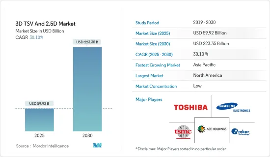
3D TSVと2.5D市場規模は、2025年に599億2,000万米ドルと推定され、予測期間(2025~2030年)のCAGRは30.1%で、2030年には2,233億5,000万米ドルに達すると予測されます。
半導体産業におけるパッケージングは、継続的な変貌を遂げています。半導体用途の成長に伴い、CMOSスケーリングの鈍化と価格の高騰により、産業はICパッケージングの先進に頼らざるを得なくなっています。3D積層技術は、AI、ML、データセンターなどの用途の要求性能を満たすソリューションです。したがって、高性能コンピューティング用途に対する要求の高まりが、予測期間にわたって主にTSV(Through Silicon Via)市場を牽引しています。
主要ハイライト
- 3D TSVパッケージング技術も牽引役となっています。現在のワイヤボンディング技術と比較してチップ間のデータ伝送時間が短縮されるため、高速化とともに消費電力が大幅に削減されます。2022年10月、TSMCは独創的な3DFabricアライアンスの立ち上げを発表しました。これはTSMCのオープンイノベーションプラットフォーム(OIP)に相当するイントロダクションであり、顧客が急増する半導体とシステムレベルの設計課題のハードルを克服するのに役立ちます。また、TSMCの3DFabric技術を使用した次世代HPCとモバイル技術の進歩の迅速な統合にも貢献します。
- 電子機器に対する消費者需要の高まりは、さまざまな新機能を実現する先進的半導体デバイスの必要性に火をつけた。半導体機器に対する要求が一貫して強まる中、先進パッケージング技術は、今日のデジタル化された世界に必要なフォームファクターと処理能力を提供しています。例えば、半導体産業協会によると、2022年8月の世界半導体産業売上高は474億米ドルで、2021年8月の合計473億米ドルから0.1%の微増となりました。
- また、GSM協会によると、2025年までに米国は世界で最もスマートフォンの普及率が高くなると予想されている(接続の49%)。米国IoT協会によると、米国は1世帯当たりのスマートホームデバイス比率が最も高く、2つまたは3つの使用事例(エネルギー、セキュリティ、民生用電子機器)にまたがる民生用電子機器製品を所有する消費者の傾向が最も顕著です。
- さらに、2022年9月、バイデン政権は、米国が国家安全保障に不可欠な世界の最先端チップの生産量ゼロ、消費量25%であることから、中国依存に対抗するため、国内半導体産業の育成に500億米ドルを投資すると発表しました。ジョー・バイデン大統領は2022年8月、中国に対する米国の競合強化の一環として、国内のハイテク製造業を後押しする2,800億米ドルのCHIPS法案に署名しました。このような半導体セグメントへの旺盛な投資は、研究市場の成長に有利な機会をもたらすと考えられます。
- MEMSとセンサの成長は、自動車や産業オートメーションなど様々な用途でセンサやディスプレイの需要が急速に高まっていることに起因しています。2022年8月、MEMSのメーカーであり、世界の半導体産業の重要な参入企業であるSTMicroelectronicsは、消費者向けスマート産業、モバイル機器、医療、小売セグメント向けに設計された第3世代のMEMSセンサを発表しました。堅牢なチップ・サイズのモーションセンサと環境センサは、今日のスマートフォンのユーザーフレンドリーな状況認識機能を実現し、ウェアラブル端末はMEMS技術で作られています。STの最新のMEMSセンサ世代は、出力精度と消費電力に関する技術的な限界を押し広げ、性能を新たなレベルに引き上げています。
- さらに、TSVデバイスの製造に関連する高コストが市場の成長を制限しています。これには、デバイスのコストだけでなく、デバイスが適切に機能するために必要な付属品や消耗品のコストも含まれます。さらに、TSVデバイスの製造に関する厳しいガイドラインや規制もコストに拍車をかけています。
- さらに、世界の半導体不足は、パンデミック後の生産能力拡大に注力する参入企業を後押ししました。例えば、SMICは、さまざまな都市に独自のチップ製造工場を建設し、2025年までに生産能力を倍増させるという積極的な計画を発表しました。また、多くのアジア太平洋の地方政府が長期的なプログラムで半導体産業に資金を提供しており、それゆえ市場成長の回復が期待されています。例えば、中国政府は国家IC投資基金2030の第2ステージの費用として約230億~300億米ドルを導入しました。
- さらに、現在進行中のロシアとウクライナの紛争は、エレクトロニクス産業に大きな影響を与えると予想されます。紛争はすでに、以前から産業に影響を及ぼしている半導体サプライチェーンの問題とチップ不足を悪化させています。この混乱は、ニッケル、パラジウム、銅、チタン、アルミニウム、鉄鉱石といった重要な原料の価格変動という形で現れ、材料不足を招く可能性があります。その結果、3D積層メモリの製造が妨げられることになります。
3D TSVと2.5D市場の動向
LEDパッケージングが著しい成長を遂げる見込み
- LEDの製品への使用が増加し、高出力、高密度、低コストのデバイスの拡大が促進されています。シリコン貫通電極(TSV)技術による3次元(3D)パッケージングは、2Dパッケージングとは異なり、高密度の垂直相互接続を可能にします。
- TSV集積回路は接続長を短くするため、寄生容量、インダクタンス、抵抗が小さくなり、モノリシック集積と多機能集積の組み合わせが効率的に行われ、高速で低消費電力の相互接続が可能になります。IEAによると、国際照明市場におけるLEDの普及率は、2025年には約76%に達し、2030年にはさらに87.4%に達すると予想されています。
- さらに、エネルギー効率の高いLEDを採用するための政府の取り組みや規則が、調査された市場を牽引しています。国際エネルギー機関(IEA)によると、照明市場におけるLEDの成長率は2025年に75.8%になると予想されています。
- LEDパッケージングの要件はもっと良くなる可能性があります。LEDチップのパッケージングへの位置が正確でないと、パッケージング機器全体の発光効率が直接影響を受ける可能性があります。決められた位置からずれると、LEDの光が反射カップから完全に反射されなくなり、LEDの明るさに影響を与えます。
- 米国エネルギー省は最近、最新技術を用いた10の検査的プロジェクトに6,100万米ドルを投資し、何千もの家庭や企業を最先端のエネルギー効率の高いネットワークに変えると発表しました。これは、白熱電球やハロゲン電球を、よりエネルギー効率の高いLED照明に切り替えることにも適用されます。その結果、LEDの拡大に伴い、米国のLEDパッケージングニーズは予測期間中に成長します。
- さらに、市場の様々な参入企業が、調査された市場で新製品を開発しています。2022年5月、Lumileds LLCはハイパワーCSP(チップスケールパッケージング)LEDを発売しました。LUXEON HL1Zはドーム型でない片面発光で、わずか1.4mm角の小さなボックスから高い発光効率(137lm/W以上)を実現します。
- LEDパッケージング用途の急速な進歩により、今後数年間は技術革新と消費が高まり、調査された市場成長が促進されると予測されます。一方、飽和度が高いため、製品の受容が制限される可能性があり、その結果、市場成長が制限されます。
アジア太平洋が大きな市場シェアを占める見込み
- アジア太平洋は、本市場において著しい成長を遂げている地域です。スマートフォンの普及率が上昇していることから、この地域は世界の主要モバイル市場の1つとなっています。
- GSM協会によると、スマートフォンのブロードバンドネットワークはアジア太平洋の人口の96%をカバーし、12億人がモバイルインターネットサービスにアクセスしています。5Gの勢いはアジア全域で続いており、現在14の市場で商用5Gサービスが利用可能です。インドやベトナムを含む他のいくつかの市場でも、今後数年で商用サービスが開始される見込みです。2025年までに、この地域全体で4億の5G接続が見込まれ、これは人口の14%以上に相当します。さらに、インダストリー4.0もアジア太平洋の最も新しい動向のひとつです。IoTデバイスと小型化は、3D TSVを活用したインダストリー4.0の重要な動向です。この地域は、スマートシティのインフラをサポートするため、IoTに多額の投資を行っています。
- 技術の開発は、民生用電子機器、通信、医療機器、通信機器、自動車の発展に貢献しています。同国では5Gの恩恵が開始され、りわけスマートフォンの需要が高まっている
- MIITによると、中国は次世代モバイルネットワークを開発するため、2022年に200万の5G基地局設置を望んでいます。MIITによると、中国本土には現在142万5,000の設置済み5G基地局があり、全国で5億人以上の5Gユーザーをサポートしており、世界で最も包括的なネットワークとなっています。同地域での5G導入の拡大は、5G対応デバイスの需要を促進し、それによって2.5Dと3D半導体パッケージングの必要性を高めると予想されます。
- さらに、CAICTによると、5Gスマートフォンの出荷台数は国内出荷台数の75.9%を記録しており、世界平均の40.7%よりも大きいです。2022年7月までに、5Gスマートフォンは中国の全携帯電話出荷台数の74%に達すると考えられます。2022年7月までの5G携帯電話の総出荷台数は124mm台で、中国は121機種の最新5G携帯電話を導入しました。このような動向は、この地域の2.5Dと3D半導体パッケージングソリューション需要を加速させると考えられます。
- 自律走行車と電気自動車の利用増加も、地域全体の先端半導体需要を増加させており、研究市場の成長をさらに後押ししています。2022年2月、Teslaは中国国内と輸出市場での需要増加に対応するため、中国に第2EV施設を建設する予定です。短期的には、Teslaは中国での生産能力を少なくとも年間100万台まで引き上げる意向で、上海臨港自由貿易区にある現在の展示会周辺に第2工場を計画しています。さらに、中国政府は2025年までに全自動車販売台数の20%を電気自動車にすることを目指しており、これには次世代の公用車としてNEVを採用することも含まれます。
- さらに、半導体製造とパッケージング工場への投資が拡大していることも、調査対象市場にとって有利な成長シナリオを生み出しています。例えば、大手半導体チップメーカーであるIntelは最近、マレーシアに先進チップパッケージング施設を建設するために70億米ドルを投資すると発表しました。同様に、2022年11月、Advanced Semiconductor Engineering(ASE)は、マレーシアの生産拠点を拡大するために3億米ドルの投資を発表しました。
3D TSVと2.5D産業概要
3D TSVと2.5D市場は競争が激しく、多様化しているため様々な重要なパフォーマーで構成されています。市場には小規模、大規模、ローカルベンダーが存在し、優れた競争を生み出しています。これらの企業は、市場シェアを拡大し収益性を高めるために、戦略的な協力関係を築いています。また、同市場の各社は、企業向けネットワーク機器技術に取り組む新興企業を買収し、製品力の強化を図っています。
2022年8月、Intelは、2.5Dと3Dベースのチップ設計を支援する独自のアーキテクチャとパッケージングのブレークスルーを披露し、チップ製造技術とその重要性における顕著な時代の到来を告げました。Intelのシステムファウンドリーモデルの特徴は、パッケージングの強化です。同組織は、2030年までにパッケージング上のトランジスタ数を1,000億個から1兆個に改善する意向です。
2022年3月、Appleは2.5Dアプローチを採用し、チップレットを利用した将来の設計への扉を開く最新のM1 Ultraデバイスの実現を後押ししました。UltraFusionと呼ばれるパッケージング・アーキテクチャは、2つのM1 Maxチップのダイをシリコン・インターポーザー上で相互接続し、1,140億トランジスタのシステムオン・ア・チップ(SoC)を構築します。これはシリコン基板とインターポーザーを利用し、2つのダイ間で2.5TB/秒の低レイテンシーとプロセッサ間帯域幅を持つ1万の相互接続で2つのダイをサポートします。また、800GB/秒のインターフェースで動作する128GBの低レイテンシー・ユニファイドメモリにも接続されています。
その他の特典
- エクセル形式の市場予測(ME)シート
- 3ヶ月間のアナリストサポート
目次
第1章 イントロダクション
- 調査の前提条件と市場の定義
- 調査範囲
第2章 調査手法
第3章 エグゼクティブサマリー
第4章 市場洞察
- 市場概要
- 産業の魅力-ポーターのファイブフォース分析
- 供給企業の交渉力
- 買い手の交渉力
- 新規参入業者の脅威
- 代替品の脅威
- 競争企業間の敵対関係の強さ
- 産業バリューチェーン分析
- マクロ経済動向の市場への影響
第5章 市場力学
- 市場促進要因
- ハイパフォーマンス・コンピューティング用途市場の拡大
- データセンターとメモリーデバイスの拡大
- 市場課題
- ICパッケージングの高単価化
第6章 技術スナップショット
第7章 市場セグメンテーション
- パッケージングタイプ別
- 3D積層メモリー
- 2.5Dインターポーザー
- TSV付きCIS
- 3D SoC
- その他のパッケージングタイプ(LED、MEMS&センサなど)
- エンドユーザー用途別
- コンシューマー・エレクトロニクス
- 自動車
- ハイパフォーマンス・コンピューティング(HPC)とネットワーキング
- その他のエンドユーザー用途
- 地域別
- 北米
- 米国
- カナダ
- 欧州
- 英国
- ドイツ
- フランス
- イタリア
- その他の欧州
- アジア太平洋
- 中国
- インド
- 日本
- オーストラリア
- 東南アジア
- その他のアジア太平洋
- その他
- 北米
第8章 競合情勢
- 企業プロファイル
- Toshiba Corp.
- Samsung Electronics Co. Ltd.
- ASE Group
- Taiwan Semiconductor Manufacturing Company Limited
- Amkor Technology, Inc.
- Pure Storage Inc.
- United Microelectronics Corp.
- STMicroelectronics NV
- Broadcom Ltd.
- Intel Corporation
- Jiangsu Changing Electronics Technology Co. Ltd.
第9章 投資分析
第10章 市場の将来
目次
The 3D TSV And 2.5D Market size is estimated at USD 59.92 billion in 2025, and is expected to reach USD 223.35 billion by 2030, at a CAGR of 30.1% during the forecast period (2025-2030).
Packaging in the semiconductor industry has noticed a continuous transformation. As the semiconductor applications are growing, the slowdown in CMOS scaling and escalating prices have forced the industry to rely on the advancement in IC packaging. 3D stacking technologies are the solution that meets the required performance of applications like AI, ML, and data centers. Therefore, the growing requirement for high-performance computing applications mainly drives the TSV (Through Silicon Via) market over the forecast period.
Key Highlights
- The 3D TSV packaging technology is also achieving traction. It reduces data transmission time between chips and the current wire bonding technology, resulting in significantly lower power consumption with faster speed. In October 2022, TSMC announced the launch of the creative 3DFabric Alliance, a considerable introduction to TSMC's Open Innovation Platform (OIP) to help customers overcome the surging hurdles of semiconductor and system-level design challenges. It will also help in gaining rapid integration of advancements for next-generation HPC and mobile technologies using TSMC's 3DFabric technologies.
- Increasing consumer demand for electronics has sparked the need for advanced semiconductor devices that enable various new capabilities. As the demands for semiconductor appliances intensify consistently, advanced packaging techniques deliver the form factor and processing power required for today's digitized world. For instance, according to the Semiconductor Industry Association, during August 2022, global semiconductor industry sales were USD 47.4 billion, a slight boost of 0.1% over the August 2021 total of USD 47.3 billion.
- In addition, according to the GSM Association, by 2025, the United States is expected to have the highest smartphone adoption globally (49% of connections). As per the United States IoT Association, it has the highest smart home device ratio per household and the most significant consumer tendency to own appliances across two or three use cases (energy, security, and appliances).
- Moreover, in September 2022, the Biden administration announced that it would invest USD 50 billion in building up the domestic semiconductor industry to counter dependency on China, as the US produces zero and consumes 25% of the world's leading-edge chips vital for its national security. President Joe Biden signed a USD 280 billion CHIPS bill in August 2022 to boost domestic high-tech manufacturing, part of his administration's push to increase US competitiveness over China. Such robust investments in the semiconductor sector would present lucrative opportunities for the growth of the studied market.
- The growth of MEMS and Sensors is attributed to the rapidly increasing demand for sensors and displays in various applications such as automotive, industrial automation, and many others. In August 2022, STMicroelectronics, a maker of MEMS and a significant player in the worldwide semiconductor industry, launched its third generation of MEMS sensors designed for consumer smart industries, mobile devices, healthcare, and retail sectors. The robust, chip-sized motion and environmental sensors power the user-friendly, context-aware features of today's smartphones, and wearables are made on MEMS technology. ST's most recent MEMS sensor generation drives technical boundaries regarding output accuracy and power consumption, elevating performance to a new level.
- Furthermore, the high costs associated with TSV device manufacturing restrict market growth. This includes not only the cost of devices but also the cost of accessories and consumables needed for their proper functioning. Moreover, the stringent guidelines and regulations governing TSV device manufacturing also add to the charges.
- Furthermore, the worldwide semiconductor shortage encouraged players to focus on expanding production capacity during a post-pandemic. For instance, the SMIC announced aggressive plans to double its production capacity by 2025 by constructing unique chip fabrication plants in different cities. Also, many Asian-Pacific local governments have funded the semiconductor industry in a long-term program, hence anticipated to regain market growth. For instance, the Chinese government introduced roughly USD 23-30 billion to pay for the second stage of its National IC Investment Fund 2030.
- Moreover, the ongoing conflict between Russia and Ukraine is expected to impact the electronics industry significantly. The conflict has already exacerbated the semiconductor supply chain issues and the chip shortage that have affected the industry for some time. The disruption may come in the form of volatile pricing for critical raw materials such as nickel, palladium, copper, titanium, aluminum, and iron ore, resulting in material shortages. This would obstruct the manufacturing of 3D Stacked Memory.
3D TSV And 2.5D Market Trends
LED Packaging Expected to Witness the Significant Growth
- The increasing use of LED in products has promoted the expansion of higher power, greater density, and lower-cost devices. Using three-dimensional (3D) packaging through silicon via (TSV) technology authorizes a high density of vertical interconnects, unlike 2D packaging.
- TSV integrated circuits reduce connection lengths; thus, smaller parasitic capacitance, inductance, and resistance are required where a combination of monolithic and multifunctional integration is done efficiently, providing high-speed, low-power interconnects. According to IEA, the penetration rate of LEDs into the international lighting market is expected to reach some 76% in 2025 and further to 87.4% in 2030.
- Further, government initiatives and rules to adopt energy-efficient LEDs drive the studied Market. According to the International Energy Agency (IEA), the growth rate of LEDs in the lighting market is anticipated to be 75.8% in 2025.
- The requirements for LED packaging could be much better. If LED chips are not positioned into the package precisely, the luminescence efficiency of the overall packaging appliance might be affected directly. Any deviation from the established position will prevent LED light from being fully reflected from the reflective cup, affecting the LED's brightness.
- The US Department of Energy recently announced investing USD 61 million in 10 pilot projects using the latest technologies to turn thousands of homes and businesses into cutting-edge, energy-efficient networks. This applies to switching out incandescent and halogen bulbs for better energy-efficient LED lighting. As a result, with the expansion in LEDs, the LED packaging need in the United States will grow in the forecasted period.
- Furthermore, various players in the market are developing new products in the studied Market. In May 2022, Lumileds LLC launched high-power CSP (chip-scale package) LED. The LUXEON HL1Z is an un-domed, single-sided emitter that delivers high luminous efficacy (137lm/W or more) from a tiny box, just 1.4mm square.
- Rapid advancements in LED package applications are projected to raise innovation and consumption in the coming years, propelling the studied market growth. On the other hand, high saturation may limit product acceptance, which, in turn, limits market growth.
Asia-Pacific is Expected to Hold the Significant Market Share
- Asia-Pacific is the significant-growing region in the Market studied. The rising smartphone adoption rates have made the region one of the major mobile markets in the world, primarily due to the increasing population evolution and urbanization.
- As per the GSM Association, smartphone broadband networks cover 96% of the population of APAC, with 1.2 billion people accessing mobile internet services. 5G momentum continues revving across the region, with commercial 5G services currently available across 14 markets. Several others, including India and Vietnam, are expected to board in the coming years. By 2025, there will be 400 million 5G connections across the region, over 14% of the population. Further, industry 4.0 is also one of Asia-Pacific's most emerging trends. IoT devices and miniaturization are important trends in Industry 4.0, utilizing 3D TSV. The region is investing heavily in IoT to support smart city infrastructure.
- Advancing technologies have contributed to the development of consumer electronics, telecom, medical devices, communication devices, and automotive. With the launch of 5G benefits in the country, the demand for smartphones, among other things, has been rising.
- According to the MIIT, China desired 2 million installed 5G base stations in 2022 to develop the country's next-generation mobile network. The Chinese mainland presently has 1.425 million installed 5G base stations that support more than 500 million 5G users nationally, making it the most comprehensive network in the world, as per MIIT. The growing implementation of 5G in the region is also expected to promote the demand for 5G-enabled devices, thereby increasing the need for 2.5D and 3D semiconductor packaging.
- Further, according to CAICT, 5G smartphone shipments are recorded for 75.9% of domestic shipments, more significant than a global average of 40.7%. By July 2022, 5G smartphones will have reached 74% of all cellphone shipments in China. The total number of 5G cell phone shipments by July 2022 was 124mm units, and China introduced 121 latest 5G mobile phone models. Such trends would accelerate the region's demand for 2.5D and 3D semiconductor packaging solutions.
- The increasing use of autonomous and electric vehicles has also increased the demand for advanced semiconductors across the region, further supporting the studied Market's growth. In February 2022, Tesla plans to build a 2nd EV facility in China to keep up with rising demand locally and in export markets. In the short term, Tesla intends to increase capacity in China to at least 1mm cars yearly, with a second plant planned around its present exhibition in Shanghai's Lingang free trade zone. In addition, the Chinese government seeks 20% of all vehicle sales to be electric by 2025, including adopting NEVs as the next generation of government vehicles.
- Moreover, the growing investments in semiconductor manufacturing and packaging plants also create a favorable growth scenario for the studied Market. For instance, Intel, a significant semiconductor chip manufacturer, recently announced a USD 7 billion investment to build an advanced chip packaging facility in Malaysia. Similarly, in November 2022, Advanced Semiconductor Engineering (ASE) announced a USD 300 million investment to expand its production site in Malaysia.
3D TSV And 2.5D Industry Overview
The 3D TSV and 2.5D market is highly competitive and consists of various significant performers as it is diversified. The existence of small, large, and local vendors in the Market creates excellent competition. These firms leverage strategic collaborative endeavors to expand their market share and increase profitability. The companies in the Market are also acquiring start-ups performing on enterprise network equipment technologies to strengthen their product capabilities.
In August 2022, Intel showcased the unique architectural and packaging breakthroughs that help 2.5D and 3D-based chip designs, ushering in a remarkable era in chipmaking technologies and their importance. Intel's system foundry model features enhanced packaging. The organization intends to improve the number of transistors on a package from 100 billion to 1 trillion by 2030.
In March 2022, Apple adopted a 2.5D approach to boost the enactment of its latest M1 Ultra device that unlocks the door to future designs utilizing chiplets. A packaging architecture called UltraFusion interconnects the die of two M1 Max chips on a silicon interposer to build a system on a chip (SoC) with 114bn transistors. This utilizes a silicon substrate and interposer that supports the two dies with 10,000 interconnects with 2.5 TB/s of low latency and inter-processor bandwidth between the die. This also connects the die to 128 GB of low-latency unified memory operating an 800 GB/s interface.
Additional Benefits:
- The market estimate (ME) sheet in Excel format
- 3 months of analyst support
TABLE OF CONTENTS
1 INTRODUCTION
- 1.1 Study Assumptions and Market Definitions
- 1.2 Scope of the Study
2 RESEARCH METHODOLOGY
3 EXECUTIVE SUMMARY
4 MARKET INSIGHTS
- 4.1 Market Overview
- 4.2 Industry Attractiveness - Porter's Five Forces Analysis
- 4.2.1 Bargaining Power of Suppliers
- 4.2.2 Bargaining Power of Buyers
- 4.2.3 Threat of New Entrants
- 4.2.4 Threat of Substitute Products
- 4.2.5 Intensity of Competitive Rivalry
- 4.3 Industry Value Chain Analysis
- 4.4 Impact of Macroeconomic Trends on the Market
5 MARKET DYNAMICS
- 5.1 Market Drivers
- 5.1.1 Expanding Market for High Performance Computing Application
- 5.1.2 Expanding Scope of Data Centers and Memory Devices
- 5.2 Market Challenges
- 5.2.1 High Unit Cost of IC Packages
6 TECHNOLOGICAL SNAPSHOT
7 MARKET SEGMENTATION
- 7.1 By Packaging Type
- 7.1.1 3D Stacked Memory
- 7.1.2 2.5D Interposer
- 7.1.3 CIS with TSV
- 7.1.4 3D SoC
- 7.1.5 Other Packaging Types ( LED, MEMS & Sensors, etc.)
- 7.2 By End User Application
- 7.2.1 Consumer Electronics
- 7.2.2 Automotive
- 7.2.3 High Performance Computing (HPC) and Networking
- 7.2.4 Other End User Applications
- 7.3 By Geography
- 7.3.1 North America
- 7.3.1.1 U.S.
- 7.3.1.2 Canada
- 7.3.2 Europe
- 7.3.2.1 United Kingdom
- 7.3.2.2 Germany
- 7.3.2.3 France
- 7.3.2.4 Italy
- 7.3.2.5 Rest of Europe
- 7.3.3 Asia-Pacific
- 7.3.3.1 China
- 7.3.3.2 India
- 7.3.3.3 Japan
- 7.3.3.4 Australia
- 7.3.3.5 South East Asia
- 7.3.3.6 Rest of Asia-Pacific
- 7.3.4 Rest of the World
- 7.3.1 North America
8 COMPETITIVE LANDSCAPE
- 8.1 Company Profiles
- 8.1.1 Toshiba Corp.
- 8.1.2 Samsung Electronics Co. Ltd.
- 8.1.3 ASE Group
- 8.1.4 Taiwan Semiconductor Manufacturing Company Limited
- 8.1.5 Amkor Technology, Inc.
- 8.1.6 Pure Storage Inc.
- 8.1.7 United Microelectronics Corp.
- 8.1.8 STMicroelectronics NV
- 8.1.9 Broadcom Ltd.
- 8.1.10 Intel Corporation
- 8.1.11 Jiangsu Changing Electronics Technology Co. Ltd.
9 INVESTMENT ANALYSIS
10 FUTURE OF THE MARKET
- 発行日
- 発行
- Mordor Intelligence
- ページ情報
- 英文 118 Pages
- 納期
- 2~3営業日