
基板:世界の市場シェア分析、産業動向と統計、成長予測(2025年~2030年)
Global Substrate - Market Share Analysis, Industry Trends & Statistics, Growth Forecasts (2025 - 2030)- 発行日
- ページ情報
- 英文 120 Pages
- 納期
- 2~3営業日
- 商品コード
- 1644468
- カスタマイズ可能 お客様のご希望に応じて、既存データの加工や未掲載情報(例:国別セグメント)の追加などの対応が可能です。詳細はお問い合わせください。
- 適宜更新あり 本レポートは最新情報反映のため適宜更新し、内容構成変更を行う場合があります。ご検討の際はお問い合わせください。
- 翻訳ツール提供対象 PDF対応AI翻訳ツールの無料貸し出しサービスのご利用が可能です
概要
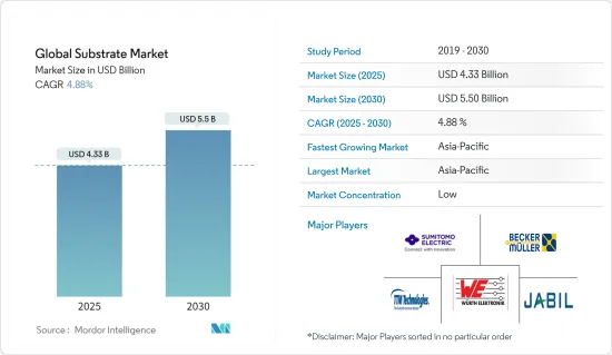
世界の基板市場規模は2025年に43億3,000万米ドルと推定され、2030年には55億米ドルに達すると予測され、予測期間(2025-2030年)のCAGRは4.88%です。
COVID-19の発生により、エレクトロニクス業界のサプライチェーンに混乱が生じ、市場成長に支障をきたしました。可処分所得が減少し、消費者心理が落ち込んだため、消費者は食品やクリーニング製品のような必需品の購入を選択し、ウェアラブルデバイスのような非必需品で高額な買い物は避けた。
主なハイライト
- COVID-19の大流行とそれに伴う半導体部品の不足は、世界経済と半導体業界に衝撃を与えました。初めて全世界とほぼすべての経済部門が影響を受け、サプライチェーンの混乱は今年以降も生産能力に悪影響を与え続けると思われます。さらに、COVID-19により、ヘルスケア・モニタリング・デバイスの需要が大幅に増加し、様々な提携が市場の成長につながった。
- フレキシブルハイブリッド・エレクトロニクス(FHE)は、印刷エレクトロニクスと従来のエレクトロニクスの長所を組み合わせた新しい電子回路製造アプローチです。この柔軟性と処理能力の組み合わせは、軽量化、新しいフォームファクターの実現、データロギングやBluetooth接続といった望ましい機能の維持につながるため、大いに望まれています。
- プリント回路基板(PCB)業界はここ数年、著しい成長を遂げているが、これは主に民生用電子機器の絶え間ない開発と、あらゆる電子機器や電気機器におけるPCB需要の増加によるものです。
- コンシューマーエレクトロニクスは、新しく、異なるPCB機能を要求しています。その開発は、PCBの形状やPCBに取り付けるアクセサリーに関連しています。PCBボードのカメラは、写真やビデオの画像処理と耐久性が主な改良点であり、大きく発展してきました。これらの小型カメラは、高解像度の画像や動画を簡単に撮影できるようになった。ボードカメラは今後数年でさらに開発され、堅牢な産業用および民生用エレクトロニクス・ソリューションを生み出すと思われます。
- 地域情勢別では、台湾、日本、中国などのアジア太平洋諸国が、世界のPCB市場の中で大きなシェアを占めています。しかし、台湾のPCB生産はここ数年減少傾向にあります。台北プリント回路協会(TPCA)によると、台湾のプリント基板市場は一時、大きな限界市場シェアで世界を席巻していました。仮に政府が世界規模で高度なプリント基板製造のハブを作り、プリント基板材料の供給における自主性を追求するとしよう。その場合、台湾は今後3~5年間、技術的優位性を保つことができます。
基板市場の動向
FHR市場では産業用が大きなシェアを占める
- また、FHE対応のソフトロボットはインダストリー4.0時代に応用されています。運動能力を失った人に運動能力を取り戻させ、職場での怪我を減らすために物体(木箱、ダンボール箱、箱など)の移動や持ち上げを補助するように設計されたロボット外骨格は、初期のソフトロボット・アプリケーションです。
- FHEの最も重要な用途のひとつは通信であり、無線技術はデータ・トランスミッションとシステム制御(IoT)に不可欠です。モノのインターネット」(IoT)という用語は、日常生活に未来的な視点を取り入れる新たなアイデアを指します。IoTは、膨大な数のインテリジェント・デバイス(センサーや情報送信機を内蔵)を接続してマシン間通信を可能にするもので、人手を介さずにクラウドと頻繁なデータ交換や更新を行う必要があり、スマートホーム、スマートヘルスケア、スマートシティ、産業、交通システムなどの分野でイノベーションを成功させることができます。
- FHEのもうひとつの応用分野は、環境景観における精密農業です。調査チームは、キトサンベースのインクを使って、フレキシブルなひずみセンサーを果実に直接印刷しました。このセンサーは果実によく接着し、機械的損傷を特定しました。グラフェン・オン・テープの調整可能なセンサーは、植物を通る水の流れを測定することができます。このセンサーは、あらかじめパターン化されたポリジメチルシロキサン(PDMS)表面にグラフェン膜を滴下し、パターン化されたグラフェン表面をターゲットテープに転写することで開発されました。
- もう1つの研究分野は、植物の健康モニタリングのための複数のセンシング機能を備えた、柔軟で伸縮可能なデバイスの開発です。さらに、報告された植物用ウェアラブルは、温度、湿度、ひずみセンサーを統合して設計されています。歪みセンサーは、PDMS基板上に薄い金金属膜を蒸着することで開発されました。温度センサーと湿度センサーは、同じフレキシブルなPI/PDMSプラットフォーム上に作製されました。
- ひずみ、インピーダンス、温度、光強度を測定する多機能農業モニタリングセンサーを開発中です。このセンサーは、CMOS、プリンタブルエレクトロニクス、転写印刷技術を組み合わせることで作製され、葉の水分、温度、ひずみ、照度センシング機能を実現しました。他の報告されているセンサーとは異なり、この伸縮可能なセンサーは葉とともに成長することができ、長期的なモニタリングに適合します。
スマート家電とウェアラブルデバイスの需要急増がSLP市場を牽引する見込み
- 民生用電子機器には、主にスマートフォン、スマートバンド、フィットネス機器、ウェアラブルが含まれます。民生用電子機器に対する需要の増加は、SLP市場のプレーヤーに展望をもたらすと期待されています。民生用電子機器の消費電力が増加しているため、バッテリーは大型化し、基板は小型化する必要があります。
- スマートフォンは、小型・薄型のICパッケージ基板なしには存在しないです。小型・薄型のICパッケージ基板は、複数の電子デバイスの機能を可能にし、すべてのデバイスを接続する多層薄型PCBも同様です。スマートフォンの機能やバッテリーの大容量化に伴い、マザーボードの高密度化や小型・軽量化が求められています。イビデンによると、MSAP(Modified Semi-Adaptiveプロセス)を採用した微細配線技術と、従来のFVSS(Full-Via Stacked Structure)で提供してきたフィルドビア積層構造を用いた技術を実現したといいます。
- ユン氏によると、ファンアウト・ウェハーレベル・パッケージは、プレミアム製品、つまり携帯電話ベンダーのスマートフォンのフラッグシップモデルに搭載されるハイエンドのアプリケーション・プロセッサー向けです。SLPは携帯電話のマザーボード向けで、このようなアセンブリに必要なスペースを削減します。ボールグリッドアレイやフリップチップパッケージは、通常、携帯電話のファインピッチスロットに使用されます。
- フレキシブルエレクトロニクスは通常、ポリエステルやポリエーテル・エーテル・ケトン(PEEK)などの柔軟なプラスチック基板上に設置された電気回路で構成されています。何度も屈曲を繰り返しても電気的接触が損なわれないようにするには、導電性トレースを高い疲労強度を持つ柔軟な金属で作るか、導電性ポリエステルで作る必要があります。この仕事に理想的な材料は、しばしばポリマーです。
- フレキシブルエレクトロニクスは、フィットネス・トラッカー、スマートウォッチ、小型のリアルタイム医療モニタリング・デバイスなどで、この拡大する産業に積極的に参加していくと思われます。人間の体はそれぞれ微妙に形が異なるため、フレキシブルエレクトロニクスは特にこの環境に適しています。接触性を確保するために機器をきつく装着する代わりに、センサーはフレキシブルエレクトロニクスのおかげで皮膚の自然なカーブに適合することができます。フレキシブルエレクトロニクスの最近の研究では、医療用途が注目されています。歩数カウンターやカロリーカウンターに加え、血圧モニター、酸素モニター、グルコースメーター、さらには血中アルコール濃度計も作られています。
- 技術が飛躍的に進歩すれば、効率的でフレキシブルなソーラーパネルが実現するかもしれないです。フレキシブルソーラー・パネルは、屋根に設置するラック以外にも、電柱、井戸のケーシング、フェンスの支柱など、同様の構造物に設置することができます。
- さらに、アップルのサプライヤーのひとつとされるZhen Ding Technologyは、超薄型・軽量が要求されるスマートフォン、ウェアラブル、その他のモバイル機器向けのSLPの需要を展望しています。SLPを使用することで、コンピューティング性能を犠牲にすることなくコンパクトな設計が可能になります。ゼンディンは、中国の工場にSLPの生産ラインを増設する計画です。
基板業界の概要
世界の基板市場は非常に断片化されています。世界のメーカーは、限られたスペースにより多くのハードウェアを配置するために、高密度相互接続(HDI)PCBなどの設計に依存してきました。HDI PCBは高性能でコアレス構造を採用しています。従来のPCBに比べ、より高密度な配線、小型化されたレーザービア、キャプチャーパッドなどを備えています。業界の既存プレーヤーは、製造能力と研究開発能力を活用して技術革新を推進し、市場での競争力を維持しています。
- 2022年10月、PCB接点用パワーエレメントのメーカーであるWurth Elektronik ICSは、試行錯誤を重ねた鉛フリー大電流接点の新世代を発表しました。PowerPlusの第2世代であるLF PowerPlus 2.0は、トルクと通電能力は第1世代と同じですが、加工がさらに容易になり、組み立て効率も向上しています。Wurth Elektronik ICSは、LF PowerPlus製品ファミリにより、プレスフィット技術アプリケーションのPCBコンタクトに信頼性が高く効果的な大電流コンタクトを提供します。特に高トルクが必要な場合や設置スペースが限られている場合に、素子を固定したり、ケーブルや部品をPCBに取り付けたりするのに最適です。
- 2022年9月、マイクロ波およびRFベースの技術スペシャリストであるTTMテクノロジーズ・インクの高周波・特殊部品ビジネスユニットは、無線周波数(「RF」)およびマイクロ波部品・半導体のピュアプレイ・プレミアディストリビューターであるRFMWと販売契約を締結しました。TTMは、RFMWを通じて、有名なXingerブランドの製品ラインナップを含むRF&S製品の全ラインナップを提供します。販売機会の特定と開発、技術的な販売サポートの提供、流通サービスも含まれます。RFMWのオンラインストアでは、TTMコンポーネントも提供されます。
その他の特典:
- エクセル形式の市場予測(ME)シート
- 3ヶ月間のアナリスト・サポート
目次
第1章 イントロダクション
- 調査の前提条件と市場定義
- 調査範囲
第2章 調査手法
第3章 エグゼクティブサマリー
第4章 プリント基板(PCB)の世界市場
- 現在の市場概要-動向/動向/市場推計・予測
- 市場成長を促進する要因
- PCB製造プロセスと技術要件
- PCBにおける技術の進歩(製造プロセスと材料の進歩)
- PCBに使用される材料とその仕様と用途
第5章 市場セグメンテーション
- 用途別
- コンピューティング
- コンシューマー
- 産業/医療
- 通信
- 自動車
- 軍事/航空宇宙
- PCBベンダー上位10社の分析
- 市場展望
第6章 フレキシブルハイブリッドエレクトロニクス(FHE)の世界市場
- 現在の市場概要-動向/力学/市場推計・予測
- 市場成長の促進要因
- FHEの製造プロセスと技術要件
- FHEの技術的進歩(製造プロセスと材料の進歩)
- FHEに使用される材料とその仕様
- FHEの技術ロードマップ
- 用途と使用事例
- 自動車および航空
- ウェアラブルおよびヘルスケア・モニタリング
- 消費財
- 産業/環境
- スマートパッケージングとRFID
- FHEベンダーの分析
- 市場の展望
第7章 世界のSLP(Substrate Like PCB)市場
- 現在の市場概要-動向/力学/市場推計・予測
- 市場成長の促進要因
- SLPの製造プロセスと技術要件
- SLPの技術進歩(製造プロセスと材料の進歩)
- SLPに使用される材料とその仕様
- SLPの技術ロードマップ
- 市場セグメンテーション
- 用途別
- コンシューマーエレクトロニクス
- 自動車
- 通信
- その他の用途
- 用途別
- SLPベンダーの分析
- 市場展望
第8章 システムインパッケージ(SIP)の世界市場
- 現在の市場概要-動向/力学/市場推計・予測
- 市場成長の促進要因
- SIPの製造プロセスと技術要件
- SIPの技術的進歩(製造プロセスと材料の進歩)
- SIPに使用される材料とその仕様
- SIPの技術ロードマップ
- 市場セグメンテーション
- 用途別
- テレコムとインフラ(サーバーと基地局)
- 自動車および輸送
- モバイルとコンシューマー
- 医療・産業
- 航空宇宙と防衛
- SIPベンダーの分析
- 市場展望
- 用途別
目次
The Global Substrate Market size is estimated at USD 4.33 billion in 2025, and is expected to reach USD 5.50 billion by 2030, at a CAGR of 4.88% during the forecast period (2025-2030).
Due to the COVID-19 outbreak, there was a disruption in the electronics industry's supply chain, which challenged market growth. With reduced disposable incomes and depressed consumer sentiment, consumers chose to buy necessities, like food and cleaning products, and avoid non-essential, big-ticket purchases, like wearable devices.
Key Highlights
- The COVID-19 pandemic and the ensuing shortage of semiconductor components proved to be a shock to the global economy and the semiconductor industry; for the first time, the entire world and nearly all economic sectors were affected, and supply chain disruptions will continue to impact production capacities negatively even in and beyond the current year. Furthermore, due to COVID-19, the demand for healthcare monitoring devices increased significantly, and various partnerships have led to market growth.
- Flexible hybrid electronics (FHE) is a novel electronic circuit manufacturing approach that combines the best of printed and conventional electronics. This combination of flexibility and processing capability is much desired since it reduces weight, enables new form factors, and maintains desirable functionality, such as data logging and Bluetooth connectivity.
- The printed circuit board (PCB) industry has experienced significant growth in the last few years, primarily owing to the continuous development of consumer electronics devices and the increasing demand for PCBs in all electronics and electrical equipment.
- Consumer electronics have been demanding new and different PCB functions. The development is related to the shape of the PCB or the accessory attached to it. PCB board cameras have developed significantly, with photo and video imaging and durability being the primary areas of improvement. These small cameras could take high-resolution images and videos with ease. Board cameras are poised to develop even further in the next few years, creating robust industry and consumer electronics solutions.
- Geographically, Asia-Pacific countries, such as Taiwan, Japan, and China, occupy a significant share of the global PCB landscape. However, PCB production in Taiwan has been on a declining trend for a few years. According to the Taipei Printed Circuit Association (TPCA), Taiwan's printed circuit board market briefly dominated the world with a large marginal market share. Suppose the government creates a hub for sophisticated PCB manufacture on a global scale and pursues autonomy in the supply of PCB materials. In that case, Taiwan can preserve its technological edge for the coming three to five years.
Substrate Market Trends
In FHR Market, Industrial to Account for a Significant Share in the Market
- Also, FHE-enabled soft robots have found applications in the Industry 4.0 era. Robotic exoskeletons designed to give mobility back to those who have lost it and assist with moving and lifting objects (e.g., crates, cartons, and boxes) to reduce workplace injury are early soft robotic applications.
- One of the most critical uses for FHE is in communication, as wireless technology is essential for data transmission and system control (IoT). The term "Internet of Things" (IoT) refers to an emerging idea that encompasses a futuristic perspective on everyday life. It connects a vast array of intelligent devices (embedded with sensors and information transmitters) to enable machine-to-machine communication, which necessitates frequent data exchange and updates to the cloud without human intervention, allowing successful innovation in areas like smart homes, smart healthcare, smart cities, industry, and transportation systems.
- Another application area for FHE is precision agriculture in the environmental landscape. Researchers printed a flexible strain sensor directly on the fruits using chitosan-based ink. These sensors provided good adhesion to the fruit and identified mechanical injuries. A graphene-on-tape adjustable sensor can measure water flow through plants. The sensor is developed by dropping a graphene film on a pre-patterned polydimethylsiloxane (PDMS) surface and then transferring the patterned graphene surface onto a target tape.
- Another research area is developing a flexible and stretchable device with multiple sensing capabilities for plant health monitoring. Further, the reported plant wearable is designed by integrating temperature, humidity, and strain sensors. The strain sensors were developed by depositing a thin gold metal film on the PDMS substrate. The temperature and humidity sensors were fabricated on the same flexible PI/PDMS platform.
- A multifunctional agricultural monitoring sensor is being developed to measure strain, impedance, temperature, and light intensity. The sensor is fabricated by combining CMOS, printable electronics, and transfer printing techniques, leading to hydration, temperature, strain, and light illuminance sensing capabilities on leaves. Unlike other reported sensors, these stretchable sensors can grow with the leaves, making them compatible with long-term monitoring.
Surge in Demand for Smart Consumer Electronics and Wearable Devices is Expected to Drive the SLP Market
- Consumer electronics mostly include smartphones, smart bands, fitness devices, and wearables. Increasing demand for consumer electronics is expected to provide prospects for players in the SLP market. Due to the increasing power consumption in consumer electronics applications, batteries need to get bigger, while boards need to get smaller.
- Smartphones would not exist without the compact, thin IC packaging substrates Compact, thin IC packaging substrates enable multiple electronic devices to function, as does the multilayer, thin PCB that connects all the devices. The advancement of smartphone functions and battery capacity requires higher densities and smaller, lighter motherboards. According to IBIDEN, it has achieved a micro-wiring technology employing the Modified Semi-Adaptive Process (MSAP) and a technique using the filled-via stack-up structure they have been offering in conventional full-via stacked structures (FVSS).
- According to Yoon, fan-out wafer-level packaging is for high-end application processors going into premium products, the flagship smartphone models for handset vendors. SLP is meant for the motherboard of phones, reducing the space needed for such assemblies. Ball grid arrays or flip-chip packages are typically used for fine-pitch slots in a phone.
- Flexible electronics typically consist of electrical circuits installed on a flexible plastic substrate, such as polyester or polyether ether ketone (PEEK). For the electrical contact to remain intact even after numerous flexing cycles, the conductive traces must either be made of a flexible metal with high fatigue strength or conductive polyester. The ideal material for the job is often a polymer.
- Flexible electronics will actively participate in this expanding industry with fitness trackers, smartwatches, and tiny, real-time medical monitoring devices. Since every human body is slightly distinct in shape, flexible electronics are especially well adapted to this environment. Instead of being compelled to wear equipment too tightly to ensure contact, sensors may now conform to the skin's natural curves thanks to flexible electronics. Medical applications have been the focus of recent research in flexible electronics. Blood pressure monitors, oxygen monitors, glucose meters, and even blood-alcohol meters are being created in addition to step counters and calorie counters.
- Efficient, flexible solar panels might become a reality as technology progresses exponentially. Flexible solar panels can be installed on surfaces other than roof-mounted racks, such as telephone poles, well casings, fence posts, and other similar structures.
- Furthermore, Zhen Ding Technology, reportedly among the suppliers of Apple, has discussed its vision of SLP demand for smartphones, wearables, and other mobile devices requiring an ultra-thin and lightweight profile. The use of SLP enables compact design without sacrificing computing performance. Zhen Ding plans to build additional SLP production lines at its factory site in China.
Substrate Industry Overview
The global substrate market is highly fragmented. Manufacturers globally have depended on designs, such as high-density interconnect (HDI) PCBs, to place more hardware in limited space. HDI PCBs use high-performance and coreless construction. Compared to traditional PCBs, they sport more densely packed wiring, miniaturized laser vias, capture pads, and other features. The industry's established players are leveraging their manufacturing capabilities and research and development capabilities to drive innovation and sustain their competitive position in the market.
- In October 2022, the manufacturer of Powerelements for PCB contacting, Wurth Elektronik ICS, launched a new generation of its tried-and-true lead-free high-current contacts: the second PowerPlus generation, LF PowerPlus 2.0, has the same torque and current-carrying capacity as the first generation but is now even easier to process and more effective to assemble. Wurth Elektronik ICS provides reliable and effective high-current contacts for PCB contact in press-fit technology applications with the LF PowerPlus product family. They are perfect for fastening elements or attaching cables and components to the PCB, especially when high torques are needed or there is limited installation space.
- In September 2022, TTM Technologies Inc.'s Radio Frequency & Specialty Components Business Unit, a microwave and RF-based technology specialist, signed a distribution agreement with RFMW, a pure play premier distributor for radio frequency ("RF") and microwave components and semiconductors. TTM will make available through RFMW the entirety of its line of RF&S goods, including its well-known Xinger brand product lineup. Opportunities will be identified and developed, technical sales support will be provided, and distribution will be included in the distribution services. The RFMW online store will also provide the TTM components.
Additional Benefits:
- The market estimate (ME) sheet in Excel format
- 3 months of analyst support
TABLE OF CONTENTS
1 INTRODUCTION
- 1.1 Study Assumptions and Market Definition
- 1.2 Scope of the Study
2 RESEARCH METHODOLOGY
3 EXECUTIVE SUMMARY
4 GLOBAL PCB MARKET
- 4.1 Current Market Overview - Trends/Dynamics/Market Demand Estimates and Projections
- 4.2 Factors Driving Market Growth
- 4.3 PCB Manufacturing Process and Technical Requirements
- 4.4 Technological Advancements in PCBs (Manufacturing Process and Materials Advancements)
- 4.5 Materials Used for PCBs along with their Specifications and Applications
5 MARKET SEGMENTATION
- 5.1 By Application
- 5.1.1 Computing
- 5.1.2 Consumer
- 5.1.3 Industrial/Medical
- 5.1.4 Communication
- 5.1.5 Automotive
- 5.1.6 Military/Aerospace
- 5.2 Analysis of Top 10 PCB Vendors
- 5.3 Market Outlook
6 GLOBAL FLEXIBLE HYBRID ELECTRONICS (FHE) MARKET
- 6.1 Current Market Overview - Trends/Dynamics/Market Demand Estimates & Projections
- 6.2 Factors Driving the Market Growth
- 6.3 FHE Manufacturing Process and Technical Requirements
- 6.4 Technological Advancement in FHE (Manufacturing Process and Materials Advancements)
- 6.5 Materials Used for FHEs along with their Specifications
- 6.6 Technological Roadmap of FHE
- 6.7 Applications and Use Cases
- 6.7.1 Automotive and Aeronautical
- 6.7.2 Wearable and Healthcare Monitoring
- 6.7.3 Consumer Goods
- 6.7.4 Industrial/Environmental
- 6.7.5 Smart Packaging and RFID
- 6.8 Analysis of FHE Vendors
- 6.9 Market Outlook
7 GLOBAL SUBSTRATE LIKE PCB (SLP) MARKET
- 7.1 Current Market Overview - Trends/Dynamics/Market Demand Estimates and Projections
- 7.2 Factors Driving the Market Growth
- 7.3 SLP Manufacturing Process and Technical Requirements
- 7.4 Technological Advancement in SLP (Manufacturing Process and Materials Advancements)
- 7.5 Materials Used for SLP with their Specifications
- 7.6 Technological Roadmap of SLP
- 7.7 MARKET SEGMENTATION
- 7.7.1 By Application
- 7.7.1.1 Consumer Electronics
- 7.7.1.2 Automotive
- 7.7.1.3 Communication
- 7.7.1.4 Other Applications
- 7.7.1 By Application
- 7.8 Analysis of SLP Vendors
- 7.9 Market Outlook
8 GLOBAL SYSTEM-IN-PACKAGE (SIP) MARKET
- 8.1 Current Market Overview - Trends/Dynamics/Market Demand Estimates and Projections
- 8.2 Factors Driving the Market Growth
- 8.3 SIP Manufacturing Process and Technical Requirements
- 8.4 Technological Advancement in SIP (Manufacturing Process and Materials Advancements)
- 8.5 Materials Used for SIP along with their Specifications
- 8.6 Technological Roadmap of SIP
- 8.7 MARKET SEGMENTATION
- 8.7.1 By Application
- 8.7.1.1 Telecom and Infrastructure (Servers and Base Stations)
- 8.7.1.2 Automotive and Transportation
- 8.7.1.3 Mobile and Consumer
- 8.7.1.4 Medical and Industrial
- 8.7.1.5 Aerospace and Defense
- 8.7.2 Analysis of SIP Vendors
- 8.7.3 Market Outlook
- 8.7.1 By Application
- 発行日
- 発行
- Mordor Intelligence
- ページ情報
- 英文 120 Pages
- 納期
- 2~3営業日


