|
|
市場調査レポート
商品コード
1689939
半導体計測・検査装置:市場シェア分析、産業動向、成長予測(2025年~2030年)Semiconductor Metrology And Inspection Equipment - Market Share Analysis, Industry Trends & Statistics, Growth Forecasts (2025 - 2030) |
||||||
|
|||||||
カスタマイズ可能
適宜更新あり
|
|||||||


| 半導体計測・検査装置:市場シェア分析、産業動向、成長予測(2025年~2030年) |
|
出版日: 2025年03月18日
発行: Mordor Intelligence
ページ情報: 英文 150 Pages
納期: 2~3営業日
|

全表示
- 概要
- 目次
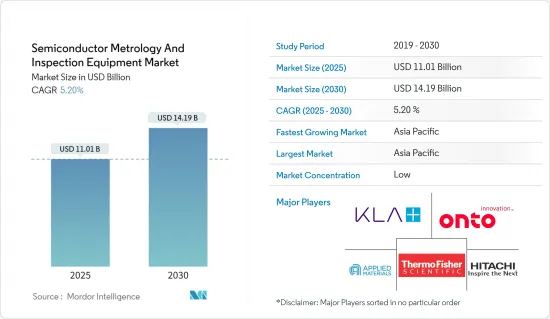
半導体計測・検査装置市場規模は2025年に110億1,000万米ドルと推定、2030年には141億9,000万米ドルに達すると予測、予測期間(2025年~2030年)のCAGRは5.2%。
主なハイライト
- 半導体の計測と検査は、半導体製造プロセスの管理において重要な役割を果たしています。半導体ウエハーの製造プロセスには約400~600の工程があり、1~2カ月で完了することもあります。工程の早い段階で欠点が見つかると、その後の工程に費やされた努力が無駄になりかねません。半導体製造工程では、特定の歩留まりを保証するために、重要な節目で計測・検査手順が実施されます。
- 浜松ホトニクスは、半導体ウエハーに対する現在の市場要求を満たすために、高い生産歩留まりを達成することの重要性を強調しています。計測と検査は、最適な品質と歩留まりを保証するために、広範な半導体製造プロセスにおいて重要な役割を果たしています。薄膜、線幅、パターン欠陥、その他の可能性のある欠陥を効率的に特性評価および測定し、あらゆる問題に迅速に対処し、高価なダウンタイムを最小限に抑えることが極めて重要です。半導体検査では、検査時間を短縮し、ウエハー上のパターンや薄膜の評価精度を向上させるために、高輝度UV光源の利用が不可欠です。
- 半導体計測は、ウエハーの物理的特性に関する詳細な情報を提供し、特定のパラメータに適合するよう製造プロセスの調整を容易にすることで、半導体製造プロセスにおいて重要な役割を果たしています。これにより、無駄を最小限に抑えながら、信頼性の高い高品質の半導体デバイスの生産が保証され、製造プロセスの経済性と持続可能性が維持されます。
- 半導体部門は、性能と速度を向上させ、よりコンパクトな集積回路を目指しており、その結果、製造技術も進歩しています。手順の正確な監視を維持することは、製造において不可欠な要素となっています。TSMC、Infineon、Qualcomm、Intelなどの企業がチップ生産への投資を拡大していることから、後工程では計測機器とサービスの需要が高まると予想されます。
- コスト効率の高い半導体材料への需要は、スマートフォン、家電製品、自動車用アプリケーションによって高まっています。これらの進歩は、無線技術(5G)や人工知能のようなイノベーションを刺激しています。さらに、IoTデバイスの採用動向が拡大し続けていることから、半導体業界はスマート製品を実現するためにIoTデバイスに投資すると予想されます。スマートデバイスの利用は増加傾向にあり、5G接続の世界の拡大とともにさらに増加すると予想されます。GSMAによると、5Gモバイル・ブロードバンド接続は2025年までに11億(11億)に達すると推定され、5Gの展開は同年までに世界人口の34%を包含すると予想されています。
- 市場で確固たる足場を築くため、ベンダーは戦略的パートナーシップを積極的に結び、先進的な多機能検査プラットフォームを構築しています。最近では、k-スペース・アソシエイツが2023年1月に最新の薄膜測定ツール、kSA XRF(蛍光X線)を発表しました。このツールは、光学的手法では確実に測定できない膜厚を正確に測定するために特別に設計されています。その有効性は、ガラスパネル、ウエハー、サセプターなど、さまざまな基板上の半導体層や誘電体層の測定で実証されています。これらの用途は、特に太陽エネルギー、発電、その他の薄膜技術の分野に関連しています。
- しかし、予測期間中の市場の成長は、セットアップコストの高さや計測システムの取り扱いに関する専門知識の不足といった要因によって効率的に阻害されると予想されます。こうした課題を克服するために、サービス指向のプレーヤーはオンデマンド計測サービスを提供し、精密寸法計測の専門分野で専門的な拡張機能を提供しています。
- さらに、調査対象市場の成長は、米国と中国の貿易紛争などのマクロ経済的要因によっても課題となっています。米国は中国に対していくつかの制裁を科し、中国が先端半導体装置にアクセスするのを妨げています。中国は同市場のサプライチェーンで重要な役割を果たしているため、こうした動向は同市場の成長に悪影響を及ぼします。
半導体計測・検査装置市場の動向
ウエハー検査が大きな成長を遂げる
- 半導体デバイスの設計が微細化するにつれて、製造歩留まり向上という課題が顕著になっています。ノードの微細化と複雑な3Dアーキテクチャの導入により、設計段階での工程が増え、複雑さが増しています。プロセスには何百もの工程があり、どの段階でも欠陥や電気的な不具合があれば、全体的な生産効率に支障をきたす可能性があります。新しい半導体設計の成功を左右する市場投入までの時間と歩留まりの重要性を考えると、ウエハー検査ツールの活用は、各段階で最適な性能を確保するために極めて重要です。
- ウエハー検査に対する需要の高まりは、今後数年間、3次元集積回路に対するニーズの高まりによって促進されると予想されます。これらの回路は、メモリーカード、スマートフォン、スマートカード、各種コンピューティングデバイスなどの小型半導体デバイスに広く使用されています。三次元回路は、速度、耐久性、低消費電力、メモリの軽量化など、製品全体の性能を高めるため、携帯家電、センサー、MEMS、工業製品など、スペースに制約のある数多くのアプリケーションで人気を集めています。
- 費用対効果の高いクラウド・コンピューティング・ソリューションの利用が可能になりつつあることから、マイクロプロセッサーやデジタル・シグナル・プロセッサーなどのロジック・デバイスの需要が増加しています。これは主に、さまざまな業界でサーバーやデータセンター・システムの利用が拡大していることが背景にあります。さらに、IoT対応デバイスの普及により、マイクロプロセッサの使用量も増加しています。これらのデバイスでは、温度制御を強化し性能を最適化するため、薄型ウエハーの利用が増加しています。これらの要因がウエハー検査市場の拡大に寄与しています。
- LEDアプリケーションに300mmウエハーが広く採用されていることも、薄型ウエハー検査市場の世界の成長を促す要因となっています。300mmウエハは歩留まりが高いため、LEDメーカーはスケールメリットを享受し、収益性を高めることができます。稼働中の300mmウエハー生産施設の数が増え続けているため、300mmウエハーの需要は大幅に急増すると予想されます。
- SEMI Silicon Manufacturers Group(SMG)が年末に行った分析によると、2023年の世界のシリコンウエハー出荷量は14.3%減少し、126億200万平方インチに達しました。また、同期間のウエハー収入は10.9%減の123億米ドルに縮小しました。しかし、2024年の回復の勢いは2026年まで続くと予想されており、将来への楽観的な見方もあります。人工知能(AI)、ハイパフォーマンス・コンピューティング(HPC)、5G、自動車、産業用アプリケーションなど、さまざまな分野でのシリコン需要の増加を背景に、ウエハー出荷量は過去最高を更新するとみられます。
- 5Gの導入と5G導入活動への投資の増加は、チップ産業におけるウエハーとウエハー検査ツールの需要をさらに促進すると予想されます。Ericsson Mobility Report 2022によると、北米は今後5年間で5G加入普及の世界的リーダーになると予測されています。同地域では2027年までに契約数の90%が5Gになると予測されています。さらに同レポートは、2027年までに西欧では加入の82%、湾岸協力会議では80%、北東アジアでは74%が5Gになると予測しています。すでに5Gの導入が始まっているインドでは、2027年までに全契約の約40%を5Gが占めると予想されています。世界的には、5Gは2027年までに全契約のほぼ半分を占め、合計44億契約に達すると予想されます。
- IT、IoT、再生可能エネルギー、EV、電気通信、その他のセクターは、今後数年間で大きく成長する見込みです。また、これらの分野は無線技術に大きく依存しています。ICや半導体の活用は、無線技術の応用を可能にします。その結果、ウエハー検査市場には多くの機会がもたらされています。Infineon、TSMC、ST、Micron、Intel、Samsung、その他の半導体業界の著名企業は、チップ生産活動に多額の投資を行っており、市場の需要拡大に大きく貢献しています。
アジア太平洋が市場を独占する
- アジア太平洋は、半導体産業において製造と消費の両面で突出した地域のひとつです。SIAによると、アジア太平洋地域は最大の半導体市場であり、中国が最も大きなシェアを占めています。エレクトロニクス分野の著しい進歩は、テレビやスマートフォンなどの電子機器への依存度の高まりと相まって、この地域でのウエハー検査の必要性を高めると予想されています。さらに、この地域に位置する企業は、ウエハー検査の利用に向けて資金を配分する用意があります。
- 半導体計測/検査装置市場では、多くの地域企業が提携やパートナーシップを結んでいます。例えば、中国のチップ製造装置メーカーである深センJT自動化設備は、中国最大のチップ開発企業であるファーウェイのHiSilicon Technologiesと5年間(2021年~2025年)の法的拘束力のある覚書を締結したと発表しました。両社は、半導体パッケージングツールの開発におけるパートナーシップを拡大し、自給自足で規制のない産業を創出することを目指しています。
- 地元半導体産業を発展させるための地域政府の取り組みも、研究対象市場の成長に有利な見通しを生み出しています。例えば、中国国務院の「国家集積回路産業開発ガイドライン」は、2030年までに同国を半導体産業の全分野で世界のリーダーにすることを目指しています。さらに、「メイド・イン・チャイナ2025」イニシアティブは、中国の将来の経済にとって不可欠な要素として、先端半導体製造に関する知識の達成を維持しています。これは、全国的な強力な製造業の戦略構築に非常に重点を置いています。
- 例えば、2023年7月、中国第2位のチップファウンドリーである華虹半導体は、212億人民元(29億5,000万米ドル)を調達する計画を明らかにしました。この戦略的な動きは、半導体供給の自給自足を達成し、米国による技術封鎖を克服しようとする中国の断固たる努力に沿ったものです。主にチップ生産に集中した初期段階とは対照的に、中国ICファンドIIは、既存の障害を克服するため、国内の半導体製造、設備、関連材料に多額の投資を行いました。
- 米国と中国の緊張が続く中、韓国は自国の半導体産業を強化するため、自国版「チップス法」の制定を計画しています。こうした緊張は、組立やパッケージングといったサービスに対する需要を生み出し、韓国が半導体産業を支えることを極めて重要なものにしています。2023年3月、韓国国会は、企業への税制優遇措置や投資の奨励を通じて、支配的な半導体産業を強化するための法案を可決しました。このような政府の取り組みにより、計測や検査などのバックエンド機器メーカーがこの地域で存在感を高める機会が増えると予想されます。
- 2023年3月、韓国の大手電子機器メーカーであるサムスンは、2042年までに龍仁(ヨンイン)の南燮(ナムサユプ)に710万平方メートルに及ぶ巨大な半導体ハブを設立するという韓国政府のイニシアチブを支援するため、今後20年間で300兆ウォン(2,308億米ドルに相当)を投資する意向を表明しました。この戦略的な動きは、競争が激化する世界半導体市場における韓国の地位を強化するためのものであり、その結果、ウエハーテスト、ATP、その他の装置などのバックエンド装置の需要を押し上げることになります。
- さらに、多くの企業がさまざまな分野で利益を上げるため、活動の拡大に注力しています。新北市政府は、オランダの半導体装置専門企業ASML Holding NVが2024年度に新北市林口区で新施設の建設を開始すると発表しました。さらに、日本の電子・半導体企業である東京エレクトロン株式会社は、台南市の南台湾サイエンスパークに事業拠点の設立を進めており、2024年末までに完成させる予定です。これらの投資は、計測・検査市場にビジネスチャンスをもたらす可能性を秘めています。
半導体計測・検査装置産業の概要
半導体計測・検査装置市場は、以下のような著名な企業で構成されています。 Applied Materials Inc., Nikon Metrology NV, and KLA Corporation. これらの企業は、市場拡大と買収に注力することで、継続的に事業規模を拡大してきました。これらの買収活動は、調査対象市場全体の成長を効果的に牽引しました。また、大手企業は、市場における地位を維持し、イノベーションを推進するために、研究開発活動に多大なリソースを投入しています。全体として、競争は依然として激しく、これは主に調査対象市場に参入している有力企業の存在感の強さに起因しています。
- 2023年12月、日立ハイテクは暗視野ウエハー欠陥検査装置の最新イノベーションであるDI4600を発表しました。この最新鋭ツールは、半導体製造ラインのパターン付きウエハー上のパーティクルや欠陥を検査するために特別に設計されています。専用サーバーを搭載したDI4600は、データ処理能力が強化され、パーティクルや欠陥の検出能力が向上しています。半導体メーカーは、この先進的なシステムを生産ラインに組み込むことで、高精度な欠陥モニタリングが可能となり、生産量の増加に伴う歩留まり向上とコスト効率向上を実現します。
- アプライドマテリアルズは2023年7月、フラウンホーファーIPMS(フォトニックマイクロシステム研究所)と先駆的な協力関係を結び、欧州における半導体計測およびプロセス解析の最高峰のテクノロジーセンターを設立すると発表しました。この革新的な拠点は、ICAPS(モノのインターネット、通信、自動車、電力、センサー)市場分野を中心に、半導体研究を加速し、欧州全域のチップメーカーやエコシステムパートナーとの研究開発活動を強化するための最先端の計測システムを提供することを目的としています。
その他の特典:
- エクセル形式の市場予測(ME)シート
- 3ヶ月間のアナリストサポート
目次
第1章 イントロダクション
- 調査の前提条件と市場定義
- 調査範囲
第2章 調査手法
第3章 エグゼクティブサマリー
第4章 市場洞察
- 市場概要
- 業界の魅力度-ポーターのファイブフォース分析
- 供給企業の交渉力
- 買い手の交渉力
- 新規参入業者の脅威
- 代替品の脅威
- 競合の程度
- 主要マクロ動向の影響評価
第5章 市場力学
- 市場促進要因
- 高性能、低コスト半導体への需要増加
- コンシューマー・エレクトロニクスにおける半導体ウエハー需要の増加
- 市場抑制要因
- セットアップコストの高さと、計測システムを効率的に扱うノウハウの不足
- 高い原材料費と製造コスト
第6章 市場セグメンテーション
- タイプ別
- リソグラフィー計測
- オーバーレイ
- 寸法測定装置
- マスク検査・計測
- ウエハー検査
- 薄膜計測
- その他のプロセス制御システム
- リソグラフィー計測
- 地域別
- 北米
- 欧州
- アジア太平洋
- 世界のその他の地域
第7章 競合情勢
- 企業プロファイル
- KLA Corporation
- Applied Materials Inc.
- Onto Innovation Inc.
- Thermo Fisher Scientific Inc.
- Hitachi Hi-Technologies Corporation(Hitachi Limited)
- Nova Measuring Instruments Ltd
- ASML Holding NV
- Lasertec Corporation
- JEOL Ltd
- Nikon Metrology NV(Nikon Group)
- Camtek Limited
第8章 投資分析
第9章 市場の将来
The Semiconductor Metrology And Inspection Equipment Market size is estimated at USD 11.01 billion in 2025, and is expected to reach USD 14.19 billion by 2030, at a CAGR of 5.2% during the forecast period (2025-2030).
Key Highlights
- Semiconductor metrology and inspection play a crucial role in the management of the semiconductor manufacturing process. The manufacturing process of semiconductor wafers involves approximately 400 to 600 steps, which can be completed within one to two months. Any shortcomings detected early on in the process can result in the wastage of all the efforts put into the subsequent steps. Metrology and inspection procedures are implemented at critical junctures of the semiconductor manufacturing process to guarantee a specific yield.
- Hamamatsu emphasizes the importance of achieving high production yields in order to satisfy the current market requirements for semiconductor wafers. Metrology and inspection play a vital role in the extensive semiconductor manufacturing process to guarantee optimal quality and yield. It is crucial to efficiently characterize and measure thin films, line widths, pattern flaws, and other possible defects to promptly address any issues and minimize expensive downtime. In semiconductor inspection, the utilization of higher radiance UV light sources is essential to reduce inspection durations and improve the precision of evaluating patterns and thin films on wafers.
- Semiconductor metrology plays a crucial role in the semiconductor manufacturing process by offering detailed information on the physical properties of the wafer and facilitating adjustments to the production process to meet specific parameters. This ensures the production of reliable semiconductor devices of high quality while minimizing wastage, thus maintaining the economic viability and sustainability of the manufacturing process.
- The semiconductor sector is continuously aiming for more compact integrated circuits that provide enhanced performance and speeds, resulting in progress in manufacturing techniques. Maintaining accurate oversight of procedures has emerged as a vital factor in manufacturing. With firms like TSMC, Infineon, Qualcomm, and Intel expanding their chip production investments, the demand for metrology equipment and services is expected to rise in the back-end process.
- The demand for cost-effective semiconductor materials is being fueled by smartphones, consumer electronics, and automotive applications. These advancements are inspiring innovations like wireless technologies (5G) and artificial intelligence. Additionally, the semiconductor industry is expected to invest in IoT devices to achieve smart products as the trend of adoption of IoT devices continues to grow. The utilization of smart devices is on the rise and is anticipated to increase further with the global expansion of 5G connections. As per the GSMA, it is estimated that 5G mobile broadband connections will reach 1,100 million (1.1 billion) by the year 2025, while the 5G deployment is expected to encompass 34% of the global population by the same year.
- In order to gain a strong foothold in the market, vendors are actively engaging in strategic partnerships to create advanced multifunction inspection platforms. Recently, k-Space Associates introduced its latest thin film metrology tool, the kSA XRF (X-ray fluorescence), in January 2023. This tool is specifically designed to accurately measure the thickness of films that cannot be reliably measured using optical methods. Its effectiveness has been demonstrated in measuring semiconductor and dielectric layers on various substrates such as glass panels, wafers, and susceptors. These applications are particularly relevant in the fields of solar energy, power generation, and other thin-film technologies.
- However, the market's growth during the forecast period is expected to be hindered efficiently by factors such as high setup costs and a lack of expertise in handling metrology systems. In order to overcome these challenges, service-oriented players are offering on-demand metrology services, providing a professional extension in the specialized field of precision dimensional metrology.
- Furthermore, the growth of the market studied is also challenged by macroeconomic factors, such as the US-China trade dispute. The United States has imposed several sanctions on China, preventing the country from accessing advanced semiconductor equipment. Since China plays a significant role in the market's supply chain, these trends negatively impact the growth of the market studied.
Semiconductor Metrology and Inspection Equipment Market Market Trends
Wafer Inspection to Witness Significant Growth
- As the design of semiconductor devices progresses toward smaller nodes, the challenge of increasing manufacturing yields becomes more pronounced. The introduction of smaller nodes and intricate 3D architectures leads to additional steps and heightened complexity in the design phase. With hundreds of steps in the process, any defect or electrical fault at any stage can impede overall production efficiency. Given the significance of time-to-market and time-to-yield in determining the success of a new semiconductor design, the utilization of wafer inspection tools is crucial to ensure optimal performance at each stage.
- The growing demand for wafer inspection is expected to be fueled by the increasing need for three-dimensional integrated circuits in the upcoming years. These circuits are widely used in small semiconductor devices such as memory cards, smartphones, smart cards, and various computing devices. Three-dimensional circuits are gaining popularity in numerous space-constrained applications like portable consumer electronics, sensors, MEMS, and industrial products, as they enhance overall product performance in terms of speed, durability, low power consumption, and lightweight memory.
- The increasing availability of cost-effective cloud computing solutions has led to a rise in demand for logic devices such as microprocessors and digital signal processors. This is primarily driven by the growing use of server and data center systems in various industries. Furthermore, the proliferation of IoT-enabled devices has resulted in a higher usage of microprocessors. Thin wafers are increasingly utilized in these devices to enhance temperature control and optimize performance. These factors collectively contribute to the expansion of the wafer inspection market.
- The widespread adoption of 300 mm wafers in LED applications is also a key driver for the global growth of the thin wafer inspection market. These wafers offer higher yields, enabling LED manufacturers to achieve economies of scale and enhance profitability. As the number of operational 300 mm wafer production facilities continues to increase, the demand for 300 mm wafers is expected to witness a significant surge.
- According to the year-end analysis conducted by the SEMI Silicon Manufacturers Group (SMG), global silicon wafer shipments experienced a decline of 14.3% in 2023, reaching 12,602 million square inches. Additionally, wafer revenue contracted by 10.9% to USD 12.3 billion during the same period. However, there is optimism for the future as the momentum from the 2024 rebound is expected to continue until 2026. This positive trend is anticipated to result in new record-high wafer shipments, driven by the increasing demand for silicon in various sectors such as artificial intelligence (AI), high-performance computing (HPC), 5G, automotive, and industrial applications.
- The introduction of 5G and increasing investments in the 5G adoption activities are further expected to drive the demand for wafers and wafer inspection tools in the chip industry. According to the Ericsson Mobility Report 2022, North America is projected to be the global leader in 5G subscription penetration over the next five years. It is anticipated that 90% of subscriptions in the region will be 5G by 2027. Additionally, the report predicts that by 2027, 82% of subscriptions in Western Europe, 80% in the Gulf Cooperation Council, and 74% in North-East Asia will be 5G. In India, where 5G deployments have already begun, it is expected that 5G will account for approximately 40% of all subscriptions by 2027. Globally, 5G is expected to represent nearly half of all subscriptions by 2027, reaching a total of 4.4 billion subscriptions.
- The IT, IoT, renewable, EVs, telecom, and other sectors are poised for substantial growth in the upcoming years. Additionally, these sectors heavily rely on wireless technology. The utilization of ICs and semiconductors enables the application of wireless technology. As a result, the wafer inspection market is presented with a multitude of opportunities. Prominent companies in the semiconductor industry, such as Infineon, TSMC, ST, Micron, Intel, Samsung, and others, are making significant investments in chip production activities, which can greatly contribute to the market's increased demand.
Asia-Pacific to Dominate the Market
- Asia-Pacific is one of the prominent regions in the semiconductor industry in terms of manufacturing and consumption. According to SIA, Asia-Pacific is the largest regional semiconductor market, and China accounts for the most significant share in the region. The significant advancements in the electronics sector, combined with the growing reliance on electronic gadgets like televisions and smartphones, are anticipated to boost the requirement for wafer inspection in the region. Furthermore, companies situated in this area are prepared to allocate funds toward the utilization of wafer inspections.
- Many regional companies are entering collaborations and partnerships in the semiconductor metrology/inspection equipment market. For instance, Shenzhen JT Automation Equipment, a chip production tool manufacturer in China, announced a legally binding five-year (2021-2025) memorandum of understanding with Huawei's HiSilicon Technologies, China's largest chip developer. Both firms aim to extend their partnership for the development of semiconductor packaging tools, creating a self-sufficient and regulated industry.
- The regional government's initiatives to develop the local semiconductor industry also create a favorable outlook for the growth of the market studied. For instance, China's State Council's "National Integrated Circuit Industry Development Guidelines" aim to make the country a global leader in all segments of the semiconductor industry by 2030. Additionally, the Made in China 2025 initiative maintains achieving knowledge concerning advanced semiconductor manufacturing as a vital component of China's future economy. It is highly focused on building a strategy for strong manufacturing nationwide.
- For instance, in July 2023, Hua Hong Semiconductor, the second-largest chip foundry in China, revealed its plan to raise CNY 21.2 billion (USD 2.95 billion). This strategic move is in line with China's determined efforts to attain self-sufficiency in semiconductor supply and overcome the technology blockade imposed by the United States. In contrast to the initial phase that primarily concentrated on chip production, the China IC Fund II has made significant investments in domestic semiconductor manufacturing, equipment, and associated materials to overcome the existing obstacles.
- South Korea plans to enact its own version of the "Chips Act" in order to bolster its semiconductor industry amid the ongoing tensions between the United States and China. These tensions have created a demand for services such as assembly and packaging, making it crucial for South Korea to support its semiconductor industry. In March 2023, the country's parliament passed legislation to strengthen its dominant semiconductor industry by providing tax benefits to businesses and encouraging investments. Such government initiatives are expected to boost the opportunities for the backend equipment markers, such as metrology and inspection, to enhance their presence in the region.
- In March 2023, Samsung, the Korean electronics giant, announced its intention to invest KRW 300 trillion (equivalent to USD 230.8 billion) over the next two decades in support of the South Korean government's initiative to establish a massive semiconductor hub spanning 7.1 million square meters in Namsayup, Yongin, by 2042. This strategic move is designed to bolster Korea's position in the increasingly competitive global semiconductor market, consequently driving up the demand for backend equipment such as wafer testing, ATP, and other equipment.
- Additionally, numerous enterprises are focusing on expanding their activities to boost profits in different sectors. The New Taipei City government announced that ASML Holding NV, a Dutch company that specializes in semiconductor equipment, will commence the construction of its new facility in the Linkou District of New Taipei City in the fiscal year 2024. Moreover, Tokyo Electron Ltd, a Japanese electronics and semiconductor corporation, is making progress in establishing its operations hub in the Southern Taiwan Science Park in Tainan, with plans to complete it by the end of 2024. These investments have the potential to create opportunities in the metrology and inspection market.
Semiconductor Metrology and Inspection Equipment Industry Overview
The semiconductor metrology and inspection equipment market comprises prominent players such as Applied Materials Inc., Nikon Metrology NV, and KLA Corporation. These firms have continuously expanded their operation scales by focusing on market expansions and acquisitions. Acquisition activities effectively set the ball rolling regarding the overall growth of the market studied. Large companies have also been expending significant resources on R&D operations to protect their market position and drive innovation in the market studied. Overall, the degree of competition remains high, primarily driven by the strong presence of prominent players involved in the market studied.
- In December 2023, Hitachi High-Tech Corporation unveiled the DI4600, the latest innovation in its Dark Field Wafer Defect Inspection System. This state-of-the-art tool is specifically designed to inspect particles and defects on patterned wafers in semiconductor production lines. With its dedicated server, the DI4600 offers enhanced data processing power, enabling improved detection capabilities for particles and defects. By incorporating this advanced system into their production lines, semiconductor manufacturers can ensure highly accurate defect monitoring, resulting in increased yields and cost efficiency as production volumes continue to rise.
- In July 2023, Applied Materials Inc. and the Fraunhofer Institute for Photonic Microsystems IPMS announced a pioneering collaboration to create the premier technology center for semiconductor metrology and process analysis in Europe. This innovative hub is designed to provide state-of-the-art metrology systems to accelerate semiconductor research and enhance development efforts with chipmakers and ecosystem partners across Europe, with a specific focus on ICAPS (Internet of Things, communications, automotive, power, and sensors) market segments.
Additional Benefits:
- The market estimate (ME) sheet in Excel format
- 3 months of analyst support
TABLE OF CONTENTS
1 INTRODUCTION
- 1.1 Study Assumptions and Market Definition
- 1.2 Scope of the Study
2 RESEARCH METHODOLOGY
3 EXECUTIVE SUMMARY
4 MARKET INSIGHTS
- 4.1 Market Overview
- 4.2 Industry Attractiveness - Porter's Five Forces Analysis
- 4.2.1 Bargaining Power of Suppliers
- 4.2.2 Bargaining Power of Buyers
- 4.2.3 Threat of New Entrants
- 4.2.4 Threat of Substitutes
- 4.2.5 Degree of Competition
- 4.3 An Assessment of the Impact of Key Macro Trends
5 MARKET DYNAMICS
- 5.1 Market Drivers
- 5.1.1 Increasing Demand for High-performance, Low-cost Semiconductors
- 5.1.2 Increasing Demand for Semiconductor Wafers in Consumer Electronics
- 5.2 Market Restraints
- 5.2.1 High Setup Cost and Lack of Expertise in Handling Metrology Systems Efficiently
- 5.2.2 High Raw Material and Fabrication Costs
6 MARKET SEGMENTATION
- 6.1 By Type
- 6.1.1 Lithography Metrology
- 6.1.1.1 Overlay
- 6.1.1.2 Dimension Equipment
- 6.1.1.3 Mask Inspection and Metrology
- 6.1.2 Wafer Inspection
- 6.1.3 Thin Film Metrology
- 6.1.4 Other Process Control Systems
- 6.1.1 Lithography Metrology
- 6.2 By Geography
- 6.2.1 North America
- 6.2.2 Europe
- 6.2.3 Asia-Pacific
- 6.2.4 Rest of the World
7 COMPETITIVE LANDSCAPE
- 7.1 Company Profiles
- 7.1.1 KLA Corporation
- 7.1.2 Applied Materials Inc.
- 7.1.3 Onto Innovation Inc.
- 7.1.4 Thermo Fisher Scientific Inc.
- 7.1.5 Hitachi Hi-Technologies Corporation (Hitachi Limited)
- 7.1.6 Nova Measuring Instruments Ltd
- 7.1.7 ASML Holding NV
- 7.1.8 Lasertec Corporation
- 7.1.9 JEOL Ltd
- 7.1.10 Nikon Metrology NV (Nikon Group)
- 7.1.11 Camtek Limited

