|
|
市場調査レポート
商品コード
1397753
半導体エッチング装置の世界市場規模、シェア、産業動向分析レポート:タイプ別、プロセス別、エンドユーザー別、地域別展望と予測、2023年~2030年Global Semiconductor Etch Equipment Market Size, Share & Industry Trends Analysis Report By Type (Dry and Wet), By Process, By End User (Integrated Device Manufacturers, Foundry and Memory Manufacturers), By Regional Outlook and Forecast, 2023 - 2030 |
||||||
|
|
|||||||
|
|||||||


| 半導体エッチング装置の世界市場規模、シェア、産業動向分析レポート:タイプ別、プロセス別、エンドユーザー別、地域別展望と予測、2023年~2030年 |
|
出版日: 2023年12月15日
発行: KBV Research
ページ情報: 英文 242 Pages
納期: 即納可能
|

- 全表示
- 概要
- 図表
- 目次
半導体エッチング装置市場規模は2030年には398億米ドルに達し、予測期間中のCAGRは8.0%の市場成長率で上昇すると予測されます。
また、少量多品種生産が進む中、半導体エッチング装置は安定した需要が見込まれます。これらの需要は主に、製品や装置のバリエーションに対応して最適な処理条件を維持しようとするバイヤーからのものです。
生産ラインにおいては、アクティブ・プロセス・コントロール・システムを搭載した次世代の高精度半導体エッチング装置が標準装備されることが予想されます。半導体エッチング装置の基本性能を向上させるため、各メーカーは半導体エッチング装置の応用分野をさらに拡大し、最終用途の消費者の需要に応えようとしています。
COVID-19の影響分析
COVID-19の蔓延により、電子産業と製造業は操業停止を余儀なくされました。製造施設は閉鎖され、影響を受けた国によって課された制限のため、サプライチェーンは世界的に妨げられました。その結果、半導体エッチング装置の製造が減少し、市場成長に悪影響を及ぼしました。また、渡航禁止や完全閉鎖による労働力不足もあり、結局、世界の半導体不足の原因となっています。半導体の製造と市場需要の減少により、半導体エッチング装置市場の成長は制限されました。このため、半導体エッチング装置市場はパンデミック期以降に回復し、急成長を遂げることができると思われます。
市場成長要因
半導体の用途拡大
半導体の用途は多岐にわたり、日常生活に欠かせないものとなりつつあります。半導体は、ノートパソコン、携帯電話、電子レンジ、冷蔵庫、ゲーム機などの家電製品に欠かせない部品です。また、デジタル時計、GOSシステム、セントラルヒーティングシステム、フィットネストラッカー、テレビなど、さまざまな製品の製造を可能にする組み込みシステムの重要な部品でもあります。半導体の特性は、熱伝導率の高い半導体など、他の用途にも有用であり、半導体は熱電用途の冷却剤としても利用されています。これによって市場の成長が促進されます。
自動車分野での使用の増加
今日の技術的に進歩した自動車では、半導体デバイスは自動車のセンシング、安全機能、ディスプレイ、制御、電力管理などの重要な機能に利用されています。電気自動車やハイブリッド車(EV)では、半導体の用途がさらに増えており、現在、大きく成長しています。半導体デバイスは、安全システムや半自律運転支援システムを可能にします。半導体は、死角検出システム、バックアップカメラ、衝突回避センサー、アダプティブクルーズコントロール、レーンチェンジアシスト、エアバッグ展開センサー、緊急ブレーキシステムなどのスマート機能を可能にします。これにより、市場の成長が促進されます。
市場抑制要因
原材料不足
チップメーカーが経験する負担は、大手市場メーカーにとっても甚大です。あらゆる業界のメーカーが、未曾有の経済情勢の中で供給と要件を満たすために奔走しました。チップメーカーにとっては、パンデミックの間、政府の操業停止やその他の制限により、生産が長期間停止しました。生産が再開されるまでに、半導体メーカーはさまざまな部門からの圧力増大に対応しなければならなかっています。多くの自然現象やその他の理由による原材料の不足や半導体の生産停止は半導体産業に影響を与え、その結果、半導体エッチング装置市場の成長が制限されました。
タイプ別展望
半導体エッチング装置市場はタイプ別にウェットとドライに区分されます。2022年の半導体エッチング装置市場では、ドライセグメントが最も高い収益シェアを占めました。これは、イオン衝撃のような物理的技術による材料の除去にドライエッチングが使用されるためです。その後、表面から材料を排出したり、表面を吹き飛ばすことのできる反応性ガス種に変換する化学プロセスが行われます。ドライエッチシステムは、微細加工や異方性に優れ、精密加工を可能にします。ドライエッチング装置のこのような特質は、近い将来、このセグメントの拡大に役立つと思われます。
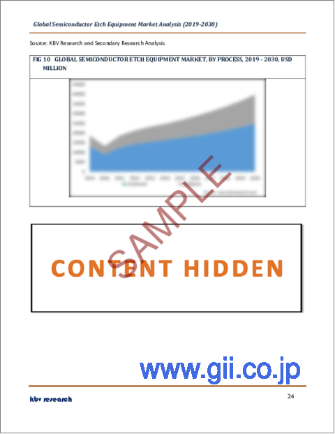
プロセス別展望
プロセス別に見ると、半導体エッチング装置市場は誘電体と導電体に分類されます。誘電体セグメントは、2022年の半導体エッチング装置市場で大幅な収益シェアを示しました。この成長は、半導体製造中に誘電体材料をエッチングするために半導体産業で使用されるためです。誘電体エッチングプロセスは、窒化シリコン、酸化シリコン、フォトレジストマスクのような様々な誘電体物質を除去する異方性プロセスです。半導体回路の小型化や高性能電子機器への需要の高まりが、予測期間中の同セグメントの成長を急増させると思われます。
エンドユーザー別展望
エンドユーザー別に見ると、半導体エッチング装置市場は集積デバイスメーカー、ファウンドリーメーカー、メモリーメーカーに二分されます。2022年の半導体エッチング装置市場では、集積デバイスメーカー部門が最も高い収益シェアを獲得しました。半導体メーカーが集積回路製品を製造、設計、販売しているためです。集積デバイスメーカーは、半導体製造を自社で行う企業を指すことが多いです。半導体とIC製品に対する需要の高まりは、集積デバイスメーカーの生産を増加させ、それによって同分野の成長を急増させる。
地域別展望
地域別では、半導体エッチング装置市場は北米、欧州、アジア太平洋、LAMEAで分析されます。アジア太平洋地域は、2022年に最大の収益シェアを獲得し、半導体エッチング装置市場をリードしました。この成長は、最も著名な半導体ファウンドリの存在によるものです。この地域の多くの国々は、半導体分野への投資を増やしており、生産とR&Dを増加させるために、新規企業や老舗企業に有利な制度やインセンティブを提供しています。消費財需要の増加に伴う技術投資の増加は、半導体エッチング装置の利用を促進し、それによって同地域の市場成長を急増させると思われます。
目次
第1章 市場範囲と調査手法
- 市場の定義
- 目的
- 市場範囲
- セグメンテーション
- 調査手法
第2章 市場要覧
- 主なハイライト
第3章 市場概要
- イントロダクション
- 概要
- 市場構成とシナリオ
- 概要
- 市場に影響を与える主な要因
- 市場促進要因
- 市場抑制要因
- ポーターファイブフォース分析
第4章 半導体エッチング装置市場における展開戦略
第5章 世界の半導体エッチング装置市場:タイプ別
- 世界のドライ市場:地域別
- 世界の生鮮市場:地域別
第6章 世界の半導体エッチング装置市場:プロセス別
- 世界の導体市場:地域別
- 世界の誘電体市場:地域別
第7章 世界の半導体エッチング装置市場:エンドユーザー別
- 世界の統合デバイスメーカー市場:地域別
- 世界の鋳造市場:地域別
- 世界のメモリメーカー市場:地域別
第8章 世界の半導体エッチング装置市場:地域別
- 北米の市場
- 北米の市場:タイプ別
- 北米のドライ市場
- 北米の生鮮市場
- 北米の市場:プロセス別
- 北米の導体市場
- 北米の誘電体市場
- 北米の市場:エンドユーザー別
- 北米の統合デバイスメーカー市場
- 北米の鋳造市場
- 北米のメモリメーカー市場
- 北米の市場:国別
- 米国の半導体エッチング装置市場
- カナダの半導体エッチング装置市場
- メキシコの半導体エッチング装置市場
- その他の北米の市場
- 北米の市場:タイプ別
- 欧州の市場
- 欧州の市場:タイプ別
- 欧州のドライ市場
- 欧州の生鮮市場
- 欧州の市場:プロセス別
- 欧州の導体市場
- 欧州の誘電体市場
- 欧州の市場:エンドユーザー別
- 欧州の統合デバイスメーカー市場
- 欧州の鋳造市場
- 欧州のメモリメーカー市場
- 欧州の市場:国別
- ドイツの半導体エッチング装置市場
- 英国の半導体エッチング装置市場
- フランスの半導体エッチング装置市場
- ロシアの半導体エッチング装置市場
- スペインの半導体エッチング装置市場
- イタリアの半導体エッチング装置市場
- その他の欧州の市場
- 欧州の市場:タイプ別
- アジア太平洋の市場
- アジア太平洋の市場:タイプ別
- アジア太平洋地域のドライ市場
- アジア太平洋地域の生鮮市場
- アジア太平洋の市場:プロセス別
- アジア太平洋地域の導体市場
- アジア太平洋地域の誘電体市場
- アジア太平洋の市場:エンドユーザー別
- アジア太平洋地域の集積デバイスメーカー市場
- アジア太平洋地域の鋳造市場
- アジア太平洋地域のメモリメーカー市場
- アジア太平洋の市場:国別
- 中国の半導体エッチング装置市場
- 日本の半導体エッチング装置市場
- インドの半導体エッチング装置市場
- 韓国の半導体エッチング装置市場
- シンガポールの半導体エッチング装置市場
- マレーシアの半導体エッチング装置市場
- その他のアジア太平洋の市場
- アジア太平洋の市場:タイプ別
- ラテンアメリカ・中東・アフリカの市場
- ラテンアメリカ・中東・アフリカの市場:タイプ別
- LAMEAのドライマーケット
- LAMEAの生鮮市場
- ラテンアメリカ・中東・アフリカの市場:プロセス別
- LAMEAの導体市場
- LAMEAの誘電体市場
- ラテンアメリカ・中東・アフリカの市場:エンドユーザー別
- LAMEAの統合デバイスメーカー市場
- LAMEA鋳造市場
- LAMEAのメモリメーカー市場
- ラテンアメリカ・中東・アフリカの市場:国別
- ブラジルの半導体エッチング装置市場
- アルゼンチン半導体エッチング装置市場
- UAEの半導体エッチング装置市場
- サウジアラビアの半導体エッチング装置市場
- 南アフリカの半導体エッチング装置市場
- ナイジェリアの半導体エッチング装置市場
- その他のラテンアメリカ・中東・アフリカの市場
- ラテンアメリカ・中東・アフリカの市場:タイプ別
第9章 企業プロファイル
- Panasonic Industry Co, Ltd.(Panasonic Holdings Corporation)
- ULVAC, Inc
- Hitachi High-Tech Corporation(Hitachi, Ltd)
- Tokyo Electron Ltd
- Applied Materials, Inc
- SPTS Technologies Ltd(KLA Corporation)
- ASML Holding NV
- Samco, Inc
- EV Group
- Suzhou Delphi Laser Co, Ltd.
- Lam Research Corporation
第10章 半導体エッチング装置市場の勝利の必須条件
LIST OF TABLES
- TABLE 1 Global Semiconductor Etch Equipment Market, 2019 - 2022, USD Million
- TABLE 2 Global Semiconductor Etch Equipment Market, 2023 - 2030, USD Million
- TABLE 3 Global Semiconductor Etch Equipment Market, By Type, 2019 - 2022, USD Million
- TABLE 4 Global Semiconductor Etch Equipment Market, By Type, 2023 - 2030, USD Million
- TABLE 5 Global Dry Market, By Region, 2019 - 2022, USD Million
- TABLE 6 Global Dry Market, By Region, 2023 - 2030, USD Million
- TABLE 7 Global Wet Market, By Region, 2019 - 2022, USD Million
- TABLE 8 Global Wet Market, By Region, 2023 - 2030, USD Million
- TABLE 9 Global Semiconductor Etch Equipment Market, By Process, 2019 - 2022, USD Million
- TABLE 10 Global Semiconductor Etch Equipment Market, By Process, 2023 - 2030, USD Million
- TABLE 11 Global Conductor Market, By Region, 2019 - 2022, USD Million
- TABLE 12 Global Conductor Market, By Region, 2023 - 2030, USD Million
- TABLE 13 Global Dielectric Market, By Region, 2019 - 2022, USD Million
- TABLE 14 Global Dielectric Market, By Region, 2023 - 2030, USD Million
- TABLE 15 Global Semiconductor Etch Equipment Market, By End User, 2019 - 2022, USD Million
- TABLE 16 Global Semiconductor Etch Equipment Market, By End User, 2023 - 2030, USD Million
- TABLE 17 Global Integrated Device Manufacturers Market, By Region, 2019 - 2022, USD Million
- TABLE 18 Global Integrated Device Manufacturers Market, By Region, 2023 - 2030, USD Million
- TABLE 19 Global Foundry Market, By Region, 2019 - 2022, USD Million
- TABLE 20 Global Foundry Market, By Region, 2023 - 2030, USD Million
- TABLE 21 Global Memory Manufacturers Market, By Region, 2019 - 2022, USD Million
- TABLE 22 Global Memory Manufacturers Market, By Region, 2023 - 2030, USD Million
- TABLE 23 Global Semiconductor Etch Equipment Market, By Region, 2019 - 2022, USD Million
- TABLE 24 Global Semiconductor Etch Equipment Market, By Region, 2023 - 2030, USD Million
- TABLE 25 North America Semiconductor Etch Equipment Market, 2019 - 2022, USD Million
- TABLE 26 North America Semiconductor Etch Equipment Market, 2023 - 2030, USD Million
- TABLE 27 North America Semiconductor Etch Equipment Market, By Type, 2019 - 2022, USD Million
- TABLE 28 North America Semiconductor Etch Equipment Market, By Type, 2023 - 2030, USD Million
- TABLE 29 North America Dry Market, By Country, 2019 - 2022, USD Million
- TABLE 30 North America Dry Market, By Country, 2023 - 2030, USD Million
- TABLE 31 North America Wet Market, By Country, 2019 - 2022, USD Million
- TABLE 32 North America Wet Market, By Country, 2023 - 2030, USD Million
- TABLE 33 North America Semiconductor Etch Equipment Market, By Process, 2019 - 2022, USD Million
- TABLE 34 North America Semiconductor Etch Equipment Market, By Process, 2023 - 2030, USD Million
- TABLE 35 North America Conductor Market, By Country, 2019 - 2022, USD Million
- TABLE 36 North America Conductor Market, By Country, 2023 - 2030, USD Million
- TABLE 37 North America Dielectric Market, By Country, 2019 - 2022, USD Million
- TABLE 38 North America Dielectric Market, By Country, 2023 - 2030, USD Million
- TABLE 39 North America Semiconductor Etch Equipment Market, By End User, 2019 - 2022, USD Million
- TABLE 40 North America Semiconductor Etch Equipment Market, By End User, 2023 - 2030, USD Million
- TABLE 41 North America Integrated Device Manufacturers Market, By Country, 2019 - 2022, USD Million
- TABLE 42 North America Integrated Device Manufacturers Market, By Country, 2023 - 2030, USD Million
- TABLE 43 North America Foundry Market, By Country, 2019 - 2022, USD Million
- TABLE 44 North America Foundry Market, By Country, 2023 - 2030, USD Million
- TABLE 45 North America Memory Manufacturers Market, By Country, 2019 - 2022, USD Million
- TABLE 46 North America Memory Manufacturers Market, By Country, 2023 - 2030, USD Million
- TABLE 47 North America Semiconductor Etch Equipment Market, By Country, 2019 - 2022, USD Million
- TABLE 48 North America Semiconductor Etch Equipment Market, By Country, 2023 - 2030, USD Million
- TABLE 49 US Semiconductor Etch Equipment Market, 2019 - 2022, USD Million
- TABLE 50 US Semiconductor Etch Equipment Market, 2023 - 2030, USD Million
- TABLE 51 US Semiconductor Etch Equipment Market, By Type, 2019 - 2022, USD Million
- TABLE 52 US Semiconductor Etch Equipment Market, By Type, 2023 - 2030, USD Million
- TABLE 53 US Semiconductor Etch Equipment Market, By Process, 2019 - 2022, USD Million
- TABLE 54 US Semiconductor Etch Equipment Market, By Process, 2023 - 2030, USD Million
- TABLE 55 US Semiconductor Etch Equipment Market, By End User, 2019 - 2022, USD Million
- TABLE 56 US Semiconductor Etch Equipment Market, By End User, 2023 - 2030, USD Million
- TABLE 57 Canada Semiconductor Etch Equipment Market, 2019 - 2022, USD Million
- TABLE 58 Canada Semiconductor Etch Equipment Market, 2023 - 2030, USD Million
- TABLE 59 Canada Semiconductor Etch Equipment Market, By Type, 2019 - 2022, USD Million
- TABLE 60 Canada Semiconductor Etch Equipment Market, By Type, 2023 - 2030, USD Million
- TABLE 61 Canada Semiconductor Etch Equipment Market, By Process, 2019 - 2022, USD Million
- TABLE 62 Canada Semiconductor Etch Equipment Market, By Process, 2023 - 2030, USD Million
- TABLE 63 Canada Semiconductor Etch Equipment Market, By End User, 2019 - 2022, USD Million
- TABLE 64 Canada Semiconductor Etch Equipment Market, By End User, 2023 - 2030, USD Million
- TABLE 65 Mexico Semiconductor Etch Equipment Market, 2019 - 2022, USD Million
- TABLE 66 Mexico Semiconductor Etch Equipment Market, 2023 - 2030, USD Million
- TABLE 67 Mexico Semiconductor Etch Equipment Market, By Type, 2019 - 2022, USD Million
- TABLE 68 Mexico Semiconductor Etch Equipment Market, By Type, 2023 - 2030, USD Million
- TABLE 69 Mexico Semiconductor Etch Equipment Market, By Process, 2019 - 2022, USD Million
- TABLE 70 Mexico Semiconductor Etch Equipment Market, By Process, 2023 - 2030, USD Million
- TABLE 71 Mexico Semiconductor Etch Equipment Market, By End User, 2019 - 2022, USD Million
- TABLE 72 Mexico Semiconductor Etch Equipment Market, By End User, 2023 - 2030, USD Million
- TABLE 73 Rest of North America Semiconductor Etch Equipment Market, 2019 - 2022, USD Million
- TABLE 74 Rest of North America Semiconductor Etch Equipment Market, 2023 - 2030, USD Million
- TABLE 75 Rest of North America Semiconductor Etch Equipment Market, By Type, 2019 - 2022, USD Million
- TABLE 76 Rest of North America Semiconductor Etch Equipment Market, By Type, 2023 - 2030, USD Million
- TABLE 77 Rest of North America Semiconductor Etch Equipment Market, By Process, 2019 - 2022, USD Million
- TABLE 78 Rest of North America Semiconductor Etch Equipment Market, By Process, 2023 - 2030, USD Million
- TABLE 79 Rest of North America Semiconductor Etch Equipment Market, By End User, 2019 - 2022, USD Million
- TABLE 80 Rest of North America Semiconductor Etch Equipment Market, By End User, 2023 - 2030, USD Million
- TABLE 81 Europe Semiconductor Etch Equipment Market, 2019 - 2022, USD Million
- TABLE 82 Europe Semiconductor Etch Equipment Market, 2023 - 2030, USD Million
- TABLE 83 Europe Semiconductor Etch Equipment Market, By Type, 2019 - 2022, USD Million
- TABLE 84 Europe Semiconductor Etch Equipment Market, By Type, 2023 - 2030, USD Million
- TABLE 85 Europe Dry Market, By Country, 2019 - 2022, USD Million
- TABLE 86 Europe Dry Market, By Country, 2023 - 2030, USD Million
- TABLE 87 Europe Wet Market, By Country, 2019 - 2022, USD Million
- TABLE 88 Europe Wet Market, By Country, 2023 - 2030, USD Million
- TABLE 89 Europe Semiconductor Etch Equipment Market, By Process, 2019 - 2022, USD Million
- TABLE 90 Europe Semiconductor Etch Equipment Market, By Process, 2023 - 2030, USD Million
- TABLE 91 Europe Conductor Market, By Country, 2019 - 2022, USD Million
- TABLE 92 Europe Conductor Market, By Country, 2023 - 2030, USD Million
- TABLE 93 Europe Dielectric Market, By Country, 2019 - 2022, USD Million
- TABLE 94 Europe Dielectric Market, By Country, 2023 - 2030, USD Million
- TABLE 95 Europe Semiconductor Etch Equipment Market, By End User, 2019 - 2022, USD Million
- TABLE 96 Europe Semiconductor Etch Equipment Market, By End User, 2023 - 2030, USD Million
- TABLE 97 Europe Integrated Device Manufacturers Market, By Country, 2019 - 2022, USD Million
- TABLE 98 Europe Integrated Device Manufacturers Market, By Country, 2023 - 2030, USD Million
- TABLE 99 Europe Foundry Market, By Country, 2019 - 2022, USD Million
- TABLE 100 Europe Foundry Market, By Country, 2023 - 2030, USD Million
- TABLE 101 Europe Memory Manufacturers Market, By Country, 2019 - 2022, USD Million
- TABLE 102 Europe Memory Manufacturers Market, By Country, 2023 - 2030, USD Million
- TABLE 103 Europe Semiconductor Etch Equipment Market, By Country, 2019 - 2022, USD Million
- TABLE 104 Europe Semiconductor Etch Equipment Market, By Country, 2023 - 2030, USD Million
- TABLE 105 Germany Semiconductor Etch Equipment Market, 2019 - 2022, USD Million
- TABLE 106 Germany Semiconductor Etch Equipment Market, 2023 - 2030, USD Million
- TABLE 107 Germany Semiconductor Etch Equipment Market, By Type, 2019 - 2022, USD Million
- TABLE 108 Germany Semiconductor Etch Equipment Market, By Type, 2023 - 2030, USD Million
- TABLE 109 Germany Semiconductor Etch Equipment Market, By Process, 2019 - 2022, USD Million
- TABLE 110 Germany Semiconductor Etch Equipment Market, By Process, 2023 - 2030, USD Million
- TABLE 111 Germany Semiconductor Etch Equipment Market, By End User, 2019 - 2022, USD Million
- TABLE 112 Germany Semiconductor Etch Equipment Market, By End User, 2023 - 2030, USD Million
- TABLE 113 UK Semiconductor Etch Equipment Market, 2019 - 2022, USD Million
- TABLE 114 UK Semiconductor Etch Equipment Market, 2023 - 2030, USD Million
- TABLE 115 UK Semiconductor Etch Equipment Market, By Type, 2019 - 2022, USD Million
- TABLE 116 UK Semiconductor Etch Equipment Market, By Type, 2023 - 2030, USD Million
- TABLE 117 UK Semiconductor Etch Equipment Market, By Process, 2019 - 2022, USD Million
- TABLE 118 UK Semiconductor Etch Equipment Market, By Process, 2023 - 2030, USD Million
- TABLE 119 UK Semiconductor Etch Equipment Market, By End User, 2019 - 2022, USD Million
- TABLE 120 UK Semiconductor Etch Equipment Market, By End User, 2023 - 2030, USD Million
- TABLE 121 France Semiconductor Etch Equipment Market, 2019 - 2022, USD Million
- TABLE 122 France Semiconductor Etch Equipment Market, 2023 - 2030, USD Million
- TABLE 123 France Semiconductor Etch Equipment Market, By Type, 2019 - 2022, USD Million
- TABLE 124 France Semiconductor Etch Equipment Market, By Type, 2023 - 2030, USD Million
- TABLE 125 France Semiconductor Etch Equipment Market, By Process, 2019 - 2022, USD Million
- TABLE 126 France Semiconductor Etch Equipment Market, By Process, 2023 - 2030, USD Million
- TABLE 127 France Semiconductor Etch Equipment Market, By End User, 2019 - 2022, USD Million
- TABLE 128 France Semiconductor Etch Equipment Market, By End User, 2023 - 2030, USD Million
- TABLE 129 Russia Semiconductor Etch Equipment Market, 2019 - 2022, USD Million
- TABLE 130 Russia Semiconductor Etch Equipment Market, 2023 - 2030, USD Million
- TABLE 131 Russia Semiconductor Etch Equipment Market, By Type, 2019 - 2022, USD Million
- TABLE 132 Russia Semiconductor Etch Equipment Market, By Type, 2023 - 2030, USD Million
- TABLE 133 Russia Semiconductor Etch Equipment Market, By Process, 2019 - 2022, USD Million
- TABLE 134 Russia Semiconductor Etch Equipment Market, By Process, 2023 - 2030, USD Million
- TABLE 135 Russia Semiconductor Etch Equipment Market, By End User, 2019 - 2022, USD Million
- TABLE 136 Russia Semiconductor Etch Equipment Market, By End User, 2023 - 2030, USD Million
- TABLE 137 Spain Semiconductor Etch Equipment Market, 2019 - 2022, USD Million
- TABLE 138 Spain Semiconductor Etch Equipment Market, 2023 - 2030, USD Million
- TABLE 139 Spain Semiconductor Etch Equipment Market, By Type, 2019 - 2022, USD Million
- TABLE 140 Spain Semiconductor Etch Equipment Market, By Type, 2023 - 2030, USD Million
- TABLE 141 Spain Semiconductor Etch Equipment Market, By Process, 2019 - 2022, USD Million
- TABLE 142 Spain Semiconductor Etch Equipment Market, By Process, 2023 - 2030, USD Million
- TABLE 143 Spain Semiconductor Etch Equipment Market, By End User, 2019 - 2022, USD Million
- TABLE 144 Spain Semiconductor Etch Equipment Market, By End User, 2023 - 2030, USD Million
- TABLE 145 Italy Semiconductor Etch Equipment Market, 2019 - 2022, USD Million
- TABLE 146 Italy Semiconductor Etch Equipment Market, 2023 - 2030, USD Million
- TABLE 147 Italy Semiconductor Etch Equipment Market, By Type, 2019 - 2022, USD Million
- TABLE 148 Italy Semiconductor Etch Equipment Market, By Type, 2023 - 2030, USD Million
- TABLE 149 Italy Semiconductor Etch Equipment Market, By Process, 2019 - 2022, USD Million
- TABLE 150 Italy Semiconductor Etch Equipment Market, By Process, 2023 - 2030, USD Million
- TABLE 151 Italy Semiconductor Etch Equipment Market, By End User, 2019 - 2022, USD Million
- TABLE 152 Italy Semiconductor Etch Equipment Market, By End User, 2023 - 2030, USD Million
- TABLE 153 Rest of Europe Semiconductor Etch Equipment Market, 2019 - 2022, USD Million
- TABLE 154 Rest of Europe Semiconductor Etch Equipment Market, 2023 - 2030, USD Million
- TABLE 155 Rest of Europe Semiconductor Etch Equipment Market, By Type, 2019 - 2022, USD Million
- TABLE 156 Rest of Europe Semiconductor Etch Equipment Market, By Type, 2023 - 2030, USD Million
- TABLE 157 Rest of Europe Semiconductor Etch Equipment Market, By Process, 2019 - 2022, USD Million
- TABLE 158 Rest of Europe Semiconductor Etch Equipment Market, By Process, 2023 - 2030, USD Million
- TABLE 159 Rest of Europe Semiconductor Etch Equipment Market, By End User, 2019 - 2022, USD Million
- TABLE 160 Rest of Europe Semiconductor Etch Equipment Market, By End User, 2023 - 2030, USD Million
- TABLE 161 Asia Pacific Semiconductor Etch Equipment Market, 2019 - 2022, USD Million
- TABLE 162 Asia Pacific Semiconductor Etch Equipment Market, 2023 - 2030, USD Million
- TABLE 163 Asia Pacific Semiconductor Etch Equipment Market, By Type, 2019 - 2022, USD Million
- TABLE 164 Asia Pacific Semiconductor Etch Equipment Market, By Type, 2023 - 2030, USD Million
- TABLE 165 Asia Pacific Dry Market, By Country, 2019 - 2022, USD Million
- TABLE 166 Asia Pacific Dry Market, By Country, 2023 - 2030, USD Million
- TABLE 167 Asia Pacific Wet Market, By Country, 2019 - 2022, USD Million
- TABLE 168 Asia Pacific Wet Market, By Country, 2023 - 2030, USD Million
- TABLE 169 Asia Pacific Semiconductor Etch Equipment Market, By Process, 2019 - 2022, USD Million
- TABLE 170 Asia Pacific Semiconductor Etch Equipment Market, By Process, 2023 - 2030, USD Million
- TABLE 171 Asia Pacific Conductor Market, By Country, 2019 - 2022, USD Million
- TABLE 172 Asia Pacific Conductor Market, By Country, 2023 - 2030, USD Million
- TABLE 173 Asia Pacific Dielectric Market, By Country, 2019 - 2022, USD Million
- TABLE 174 Asia Pacific Dielectric Market, By Country, 2023 - 2030, USD Million
- TABLE 175 Asia Pacific Semiconductor Etch Equipment Market, By End User, 2019 - 2022, USD Million
- TABLE 176 Asia Pacific Semiconductor Etch Equipment Market, By End User, 2023 - 2030, USD Million
- TABLE 177 Asia Pacific Integrated Device Manufacturers Market, By Country, 2019 - 2022, USD Million
- TABLE 178 Asia Pacific Integrated Device Manufacturers Market, By Country, 2023 - 2030, USD Million
- TABLE 179 Asia Pacific Foundry Market, By Country, 2019 - 2022, USD Million
- TABLE 180 Asia Pacific Foundry Market, By Country, 2023 - 2030, USD Million
- TABLE 181 Asia Pacific Memory Manufacturers Market, By Country, 2019 - 2022, USD Million
- TABLE 182 Asia Pacific Memory Manufacturers Market, By Country, 2023 - 2030, USD Million
- TABLE 183 Asia Pacific Semiconductor Etch Equipment Market, By Country, 2019 - 2022, USD Million
- TABLE 184 Asia Pacific Semiconductor Etch Equipment Market, By Country, 2023 - 2030, USD Million
- TABLE 185 China Semiconductor Etch Equipment Market, 2019 - 2022, USD Million
- TABLE 186 China Semiconductor Etch Equipment Market, 2023 - 2030, USD Million
- TABLE 187 China Semiconductor Etch Equipment Market, By Type, 2019 - 2022, USD Million
- TABLE 188 China Semiconductor Etch Equipment Market, By Type, 2023 - 2030, USD Million
- TABLE 189 China Semiconductor Etch Equipment Market, By Process, 2019 - 2022, USD Million
- TABLE 190 China Semiconductor Etch Equipment Market, By Process, 2023 - 2030, USD Million
- TABLE 191 China Semiconductor Etch Equipment Market, By End User, 2019 - 2022, USD Million
- TABLE 192 China Semiconductor Etch Equipment Market, By End User, 2023 - 2030, USD Million
- TABLE 193 Japan Semiconductor Etch Equipment Market, 2019 - 2022, USD Million
- TABLE 194 Japan Semiconductor Etch Equipment Market, 2023 - 2030, USD Million
- TABLE 195 Japan Semiconductor Etch Equipment Market, By Type, 2019 - 2022, USD Million
- TABLE 196 Japan Semiconductor Etch Equipment Market, By Type, 2023 - 2030, USD Million
- TABLE 197 Japan Semiconductor Etch Equipment Market, By Process, 2019 - 2022, USD Million
- TABLE 198 Japan Semiconductor Etch Equipment Market, By Process, 2023 - 2030, USD Million
- TABLE 199 Japan Semiconductor Etch Equipment Market, By End User, 2019 - 2022, USD Million
- TABLE 200 Japan Semiconductor Etch Equipment Market, By End User, 2023 - 2030, USD Million
- TABLE 201 India Semiconductor Etch Equipment Market, 2019 - 2022, USD Million
- TABLE 202 India Semiconductor Etch Equipment Market, 2023 - 2030, USD Million
- TABLE 203 India Semiconductor Etch Equipment Market, By Type, 2019 - 2022, USD Million
- TABLE 204 India Semiconductor Etch Equipment Market, By Type, 2023 - 2030, USD Million
- TABLE 205 India Semiconductor Etch Equipment Market, By Process, 2019 - 2022, USD Million
- TABLE 206 India Semiconductor Etch Equipment Market, By Process, 2023 - 2030, USD Million
- TABLE 207 India Semiconductor Etch Equipment Market, By End User, 2019 - 2022, USD Million
- TABLE 208 India Semiconductor Etch Equipment Market, By End User, 2023 - 2030, USD Million
- TABLE 209 South Korea Semiconductor Etch Equipment Market, 2019 - 2022, USD Million
- TABLE 210 South Korea Semiconductor Etch Equipment Market, 2023 - 2030, USD Million
- TABLE 211 South Korea Semiconductor Etch Equipment Market, By Type, 2019 - 2022, USD Million
- TABLE 212 South Korea Semiconductor Etch Equipment Market, By Type, 2023 - 2030, USD Million
- TABLE 213 South Korea Semiconductor Etch Equipment Market, By Process, 2019 - 2022, USD Million
- TABLE 214 South Korea Semiconductor Etch Equipment Market, By Process, 2023 - 2030, USD Million
- TABLE 215 South Korea Semiconductor Etch Equipment Market, By End User, 2019 - 2022, USD Million
- TABLE 216 South Korea Semiconductor Etch Equipment Market, By End User, 2023 - 2030, USD Million
- TABLE 217 Singapore Semiconductor Etch Equipment Market, 2019 - 2022, USD Million
- TABLE 218 Singapore Semiconductor Etch Equipment Market, 2023 - 2030, USD Million
- TABLE 219 Singapore Semiconductor Etch Equipment Market, By Type, 2019 - 2022, USD Million
- TABLE 220 Singapore Semiconductor Etch Equipment Market, By Type, 2023 - 2030, USD Million
- TABLE 221 Singapore Semiconductor Etch Equipment Market, By Process, 2019 - 2022, USD Million
- TABLE 222 Singapore Semiconductor Etch Equipment Market, By Process, 2023 - 2030, USD Million
- TABLE 223 Singapore Semiconductor Etch Equipment Market, By End User, 2019 - 2022, USD Million
- TABLE 224 Singapore Semiconductor Etch Equipment Market, By End User, 2023 - 2030, USD Million
- TABLE 225 Malaysia Semiconductor Etch Equipment Market, 2019 - 2022, USD Million
- TABLE 226 Malaysia Semiconductor Etch Equipment Market, 2023 - 2030, USD Million
- TABLE 227 Malaysia Semiconductor Etch Equipment Market, By Type, 2019 - 2022, USD Million
- TABLE 228 Malaysia Semiconductor Etch Equipment Market, By Type, 2023 - 2030, USD Million
- TABLE 229 Malaysia Semiconductor Etch Equipment Market, By Process, 2019 - 2022, USD Million
- TABLE 230 Malaysia Semiconductor Etch Equipment Market, By Process, 2023 - 2030, USD Million
- TABLE 231 Malaysia Semiconductor Etch Equipment Market, By End User, 2019 - 2022, USD Million
- TABLE 232 Malaysia Semiconductor Etch Equipment Market, By End User, 2023 - 2030, USD Million
- TABLE 233 Rest of Asia Pacific Semiconductor Etch Equipment Market, 2019 - 2022, USD Million
- TABLE 234 Rest of Asia Pacific Semiconductor Etch Equipment Market, 2023 - 2030, USD Million
- TABLE 235 Rest of Asia Pacific Semiconductor Etch Equipment Market, By Type, 2019 - 2022, USD Million
- TABLE 236 Rest of Asia Pacific Semiconductor Etch Equipment Market, By Type, 2023 - 2030, USD Million
- TABLE 237 Rest of Asia Pacific Semiconductor Etch Equipment Market, By Process, 2019 - 2022, USD Million
- TABLE 238 Rest of Asia Pacific Semiconductor Etch Equipment Market, By Process, 2023 - 2030, USD Million
- TABLE 239 Rest of Asia Pacific Semiconductor Etch Equipment Market, By End User, 2019 - 2022, USD Million
- TABLE 240 Rest of Asia Pacific Semiconductor Etch Equipment Market, By End User, 2023 - 2030, USD Million
- TABLE 241 LAMEA Semiconductor Etch Equipment Market, 2019 - 2022, USD Million
- TABLE 242 LAMEA Semiconductor Etch Equipment Market, 2023 - 2030, USD Million
- TABLE 243 LAMEA Semiconductor Etch Equipment Market, By Type, 2019 - 2022, USD Million
- TABLE 244 LAMEA Semiconductor Etch Equipment Market, By Type, 2023 - 2030, USD Million
- TABLE 245 LAMEA Dry Market, By Country, 2019 - 2022, USD Million
- TABLE 246 LAMEA Dry Market, By Country, 2023 - 2030, USD Million
- TABLE 247 LAMEA Wet Market, By Country, 2019 - 2022, USD Million
- TABLE 248 LAMEA Wet Market, By Country, 2023 - 2030, USD Million
- TABLE 249 LAMEA Semiconductor Etch Equipment Market, By Process, 2019 - 2022, USD Million
- TABLE 250 LAMEA Semiconductor Etch Equipment Market, By Process, 2023 - 2030, USD Million
- TABLE 251 LAMEA Conductor Market, By Country, 2019 - 2022, USD Million
- TABLE 252 LAMEA Conductor Market, By Country, 2023 - 2030, USD Million
- TABLE 253 LAMEA Dielectric Market, By Country, 2019 - 2022, USD Million
- TABLE 254 LAMEA Dielectric Market, By Country, 2023 - 2030, USD Million
- TABLE 255 LAMEA Semiconductor Etch Equipment Market, By End User, 2019 - 2022, USD Million
- TABLE 256 LAMEA Semiconductor Etch Equipment Market, By End User, 2023 - 2030, USD Million
- TABLE 257 LAMEA Integrated Device Manufacturers Market, By Country, 2019 - 2022, USD Million
- TABLE 258 LAMEA Integrated Device Manufacturers Market, By Country, 2023 - 2030, USD Million
- TABLE 259 LAMEA Foundry Market, By Country, 2019 - 2022, USD Million
- TABLE 260 LAMEA Foundry Market, By Country, 2023 - 2030, USD Million
- TABLE 261 LAMEA Memory Manufacturers Market, By Country, 2019 - 2022, USD Million
- TABLE 262 LAMEA Memory Manufacturers Market, By Country, 2023 - 2030, USD Million
- TABLE 263 LAMEA Semiconductor Etch Equipment Market, By Country, 2019 - 2022, USD Million
- TABLE 264 LAMEA Semiconductor Etch Equipment Market, By Country, 2023 - 2030, USD Million
- TABLE 265 Brazil Semiconductor Etch Equipment Market, 2019 - 2022, USD Million
- TABLE 266 Brazil Semiconductor Etch Equipment Market, 2023 - 2030, USD Million
- TABLE 267 Brazil Semiconductor Etch Equipment Market, By Type, 2019 - 2022, USD Million
- TABLE 268 Brazil Semiconductor Etch Equipment Market, By Type, 2023 - 2030, USD Million
- TABLE 269 Brazil Semiconductor Etch Equipment Market, By Process, 2019 - 2022, USD Million
- TABLE 270 Brazil Semiconductor Etch Equipment Market, By Process, 2023 - 2030, USD Million
- TABLE 271 Brazil Semiconductor Etch Equipment Market, By End User, 2019 - 2022, USD Million
- TABLE 272 Brazil Semiconductor Etch Equipment Market, By End User, 2023 - 2030, USD Million
- TABLE 273 Argentina Semiconductor Etch Equipment Market, 2019 - 2022, USD Million
- TABLE 274 Argentina Semiconductor Etch Equipment Market, 2023 - 2030, USD Million
- TABLE 275 Argentina Semiconductor Etch Equipment Market, By Type, 2019 - 2022, USD Million
- TABLE 276 Argentina Semiconductor Etch Equipment Market, By Type, 2023 - 2030, USD Million
- TABLE 277 Argentina Semiconductor Etch Equipment Market, By Process, 2019 - 2022, USD Million
- TABLE 278 Argentina Semiconductor Etch Equipment Market, By Process, 2023 - 2030, USD Million
- TABLE 279 Argentina Semiconductor Etch Equipment Market, By End User, 2019 - 2022, USD Million
- TABLE 280 Argentina Semiconductor Etch Equipment Market, By End User, 2023 - 2030, USD Million
- TABLE 281 UAE Semiconductor Etch Equipment Market, 2019 - 2022, USD Million
- TABLE 282 UAE Semiconductor Etch Equipment Market, 2023 - 2030, USD Million
- TABLE 283 UAE Semiconductor Etch Equipment Market, By Type, 2019 - 2022, USD Million
- TABLE 284 UAE Semiconductor Etch Equipment Market, By Type, 2023 - 2030, USD Million
- TABLE 285 UAE Semiconductor Etch Equipment Market, By Process, 2019 - 2022, USD Million
- TABLE 286 UAE Semiconductor Etch Equipment Market, By Process, 2023 - 2030, USD Million
- TABLE 287 UAE Semiconductor Etch Equipment Market, By End User, 2019 - 2022, USD Million
- TABLE 288 UAE Semiconductor Etch Equipment Market, By End User, 2023 - 2030, USD Million
- TABLE 289 Saudi Arabia Semiconductor Etch Equipment Market, 2019 - 2022, USD Million
- TABLE 290 Saudi Arabia Semiconductor Etch Equipment Market, 2023 - 2030, USD Million
- TABLE 291 Saudi Arabia Semiconductor Etch Equipment Market, By Type, 2019 - 2022, USD Million
- TABLE 292 Saudi Arabia Semiconductor Etch Equipment Market, By Type, 2023 - 2030, USD Million
- TABLE 293 Saudi Arabia Semiconductor Etch Equipment Market, By Process, 2019 - 2022, USD Million
- TABLE 294 Saudi Arabia Semiconductor Etch Equipment Market, By Process, 2023 - 2030, USD Million
- TABLE 295 Saudi Arabia Semiconductor Etch Equipment Market, By End User, 2019 - 2022, USD Million
- TABLE 296 Saudi Arabia Semiconductor Etch Equipment Market, By End User, 2023 - 2030, USD Million
- TABLE 297 South Africa Semiconductor Etch Equipment Market, 2019 - 2022, USD Million
- TABLE 298 South Africa Semiconductor Etch Equipment Market, 2023 - 2030, USD Million
- TABLE 299 South Africa Semiconductor Etch Equipment Market, By Type, 2019 - 2022, USD Million
- TABLE 300 South Africa Semiconductor Etch Equipment Market, By Type, 2023 - 2030, USD Million
- TABLE 301 South Africa Semiconductor Etch Equipment Market, By Process, 2019 - 2022, USD Million
- TABLE 302 South Africa Semiconductor Etch Equipment Market, By Process, 2023 - 2030, USD Million
- TABLE 303 South Africa Semiconductor Etch Equipment Market, By End User, 2019 - 2022, USD Million
- TABLE 304 South Africa Semiconductor Etch Equipment Market, By End User, 2023 - 2030, USD Million
- TABLE 305 Nigeria Semiconductor Etch Equipment Market, 2019 - 2022, USD Million
- TABLE 306 Nigeria Semiconductor Etch Equipment Market, 2023 - 2030, USD Million
- TABLE 307 Nigeria Semiconductor Etch Equipment Market, By Type, 2019 - 2022, USD Million
- TABLE 308 Nigeria Semiconductor Etch Equipment Market, By Type, 2023 - 2030, USD Million
- TABLE 309 Nigeria Semiconductor Etch Equipment Market, By Process, 2019 - 2022, USD Million
- TABLE 310 Nigeria Semiconductor Etch Equipment Market, By Process, 2023 - 2030, USD Million
- TABLE 311 Nigeria Semiconductor Etch Equipment Market, By End User, 2019 - 2022, USD Million
- TABLE 312 Nigeria Semiconductor Etch Equipment Market, By End User, 2023 - 2030, USD Million
- TABLE 313 Rest of LAMEA Semiconductor Etch Equipment Market, 2019 - 2022, USD Million
- TABLE 314 Rest of LAMEA Semiconductor Etch Equipment Market, 2023 - 2030, USD Million
- TABLE 315 Rest of LAMEA Semiconductor Etch Equipment Market, By Type, 2019 - 2022, USD Million
- TABLE 316 Rest of LAMEA Semiconductor Etch Equipment Market, By Type, 2023 - 2030, USD Million
- TABLE 317 Rest of LAMEA Semiconductor Etch Equipment Market, By Process, 2019 - 2022, USD Million
- TABLE 318 Rest of LAMEA Semiconductor Etch Equipment Market, By Process, 2023 - 2030, USD Million
- TABLE 319 Rest of LAMEA Semiconductor Etch Equipment Market, By End User, 2019 - 2022, USD Million
- TABLE 320 Rest of LAMEA Semiconductor Etch Equipment Market, By End User, 2023 - 2030, USD Million
- TABLE 321 Key Information - Panasonic Industry Co., Ltd.
- TABLE 322 Key Information - ULVAC, Inc.
- TABLE 323 Key Information - Hitachi High-Tech Corporation
- TABLE 324 Key Information - Tokyo Electron Ltd.
- TABLE 325 Key Information - Applied Materials, Inc.
- TABLE 326 Key Information - SPTS Technologies Ltd.
- TABLE 327 Key Information - ASML Holding N.V.
- TABLE 328 Key Information - Samco, Inc.
- TABLE 329 Key Information - EV Group
- TABLE 330 Key Information - Suzhou Delphi Laser Co., Ltd.
- TABLE 331 Key Information - Lam Research Corporation
The Global Semiconductor Etch Equipment Market size is expected to reach $39.8 billion by 2030, rising at a market growth of 8.0% CAGR during the forecast period.
In fabrication of semiconductor devices, etching is known as a technology that will selectively remove material from a thin film on a substrate (with or without prior structure on its surface) and, by this removal, a pattern is created of that material on the substrate. The etching process is resistant to the pattern which is defined by a mask.
When the mask is in place, etching of the material that is not protected by the mask can occur by dry physical or wet chemical methods. Semiconductor etch equipment removes layers from the silicon wafer's surface through various chemicals. The requirement for semiconductor etches equipment is rising significantly due to the continuously growing precision requirement of semiconductor devices.
In addition, as the manufacturing trend toward low-volume diversified production continues to advance, semiconductor etches equipment will witness consistent demand. These demands will majorly be from buyers looking to maintain optimum processing conditions in response to variations in products and equipment.
In the production line, the high-precision semiconductor etches equipment of next generation, fitted with the active process control system is expected to become a standard feature. To enhance the basic performance of semiconductor, etch equipment, the manufacturers will further increase the application area of semiconductor etch equipment striving to meet the end-use consumer's demand.
COVID-19 Impact Analysis
The outspread of COVID-19 enforced the electronic, and manufacturing industries to shut down and halt their work. Manufacturing facilties were shut down, and the supply chain was hampered globally, due to the restrictions imposed by the affected nations. All this resulted in reduction of the manufacturing of semiconductor etch equipment, thereby negatively effecting the market growth. Also, there were shortages in the workforce due to travel bans and complete lockdowns, which at the end became the reason for shortage of semiconductors globally. With the decline in the manufacturing of semiconductors and their demand in the market, the growth of the semiconductor etch equipment market was restricted. Which will aid the semiconductor etch equipment market to recovery and surge its growth after the pandemic period.
Market Growth Factors
Wider Usage of Semiconductors
The application of semiconductors is wide-ranging and becoming increasingly essential to day-to-day life. Semiconductors are critical components in consumer electronics, including laptops, mobile phones, microwaves, refrigerators, gaming consoles, and more. They are also essential components of embedded systems that make it possible to produce various products like digital watches, GOS systems, central heating systems, fitness trackers, televisions etc. The properties of semiconductors make them useful for other applications, such as those with high thermal conductivity, as semiconductors are also utilized as cooling agents in thermoelectric applications. Thereby propelling the market's growth.
The increasing usage in automotive sector
In today's technologically advanced automobiles, semiconductor devices are utilized for critical functions, like sensing, safety features, displays, control, and power management of the vehicle. There are more applications of semiconductors in electric and hybrid vehicles (EVs), which are now growing majorly. Semiconductors devices enable safety systems and semi-autonomous driver assistance systems. Semiconductors allows smart functions, which are blind-spot detection systems, backup cameras, collision-avoidance sensors, adaptive cruise controls, lane-change assist, airbag deployment sensors, and emergency braking systems. Thereby propelling the market's growth.
Market Restraining Factors
The shortage of raw material
The burden that chipmakers experience is enormous, even for major market players. Manufacturers in all industries scrambled to meet the supply and requirements in an unprecedented economic climate. For chipmakers, production during the pandemic was halted for an extended period due to government shutdowns and other restrictions. By the time production resumed, semiconductor companies had to adjust to the increased pressure from various sectors. The lack of raw materials and the halt in the production of semiconductors due to many natural causes and other reasons affected the semiconductor industries, which in turn restricted the semiconductor etch equipment market's growth.
Type Outlook
Based on type, the semiconductor etch equipment market is segmented into wet and dry. The dry segment held the highest revenue share in the semiconductor etch equipment market in 2022. This is due to the usage of dry etching in the removal of material by physical techniques such as ion impact. It is followed by material expulsion from the surface or chemical processes that convert the surface to reactive gaseous species that can be blown away. Dry etch systems are excellent in microfabrication and anisotropic and enable precision processing. These qualities of the dry etch equipment will aid in the segment's expansion in near future.
Process Outlook
By process, the semiconductor etch equipment market is classified into dielectric and conductor. The dielectric segment witnessed a substantial revenue share in the semiconductor etch equipment market in 2022. The growth is due to their usage in the semiconductor industry for etching dielectric material during semiconductor manufacturing. The dielectric etching process is an anisotropic process that removes various dielectric substances like silicon nitride, silicon oxide, and overlying photoresist masks. The rising demand for miniaturizing semiconductors circuits and high-performance electronic gadgets will surge the segment's growth in the forecasted period.
End-User Outlook
Based on end-user, the semiconductor etch equipment market is bifurcated into integrated device manufacturers, foundry and memory manufacturers. The integrated device manufacturers segment generated the highest revenue share in the semiconductor etch equipment market in 2022. The growth is because semiconductor companies manufacture, design, and sell integrated circuit products. An integrated device manufacturer is often referred to as companies that handles the semiconductor manufacturing in-house. The rising demand for semiconductors and IC products will increase the production in the integrated device manufacturers, thereby surging segment's growth.
Regional Outlook
Region-wise, the semiconductor etch equipment market is analyzed across North America, Europe, Asia Pacific, and LAMEA. The Asia-Pacific region led the semiconductor etch equipment market by generating maximum revenue share in 2022. The growth is due to the presence of the most prominent semiconductor foundries. Many nations in the region are increasingly investing in the semiconductor sector and providing lucrative schemes and incentives for new and well-established companies to increase production and R&D. The rising technological investment with the increasing demand for consumer goods will propel the semiconductor etch equipment usage and thereby surging the market's growth in the region.
The market research report covers the analysis of key stake holders of the market. Key companies profiled in the report include Panasonic Industry Co., Ltd. (Panasonic Holdings Corporation), ULVAC, Inc., Hitachi High-Tech Corporation (Hitachi, Ltd.), Tokyo Electron Ltd., Applied Materials, Inc., SPTS Technologies Ltd. (KLA Corporation), ASML Holding N.V., Samco, Inc., EV Group, Suzhou Delphi Laser Co., Ltd and Lam Research Corporation.
Semiconductor Etch Equipment Market Report Coverage:
Report Attribute Details
Market size value in 2022 USD 21.4 Billion
Market size forecast in 2030 USD 39.8 Billion
Base Year 2022
Historical period 2019 to 2021
Forecast Period 2023 to 2030
Revenue Growth Rate CAGR of 8% from 2023 to 2030
Number of Pages 242
Tables 331
Report coverage Market Trends, Revenue Estimation and Forecast, Segmentation Analysis, Regional and Country Breakdown, Companies Strategic Developments, Company Profiling
Segments covered Type, Process, End User, Region
Country scope US, Canada, Mexico, Germany, UK, France, Russia, Spain, Italy, China, Japan, India, South Korea, Singapore, Malaysia, Brazil, Argentina, UAE, Saudi Arabia, South Africa, Nigeria
Growth Drivers * Wider Usage of Semiconductors
* Increasing usage in automotive sector
Restraints * Shortage of raw material
Strategies Deployed in Semiconductor Etch Equipment Market
2023-Jun: Lam Research Corporation unveiled Coronus DX, a bevel deposition solution in the industry. Coronus DX designed to effectively tackle major manufacturing hurdles in next-gen logic, 3D NAND, and advanced packaging applications. With the launch of Coronus DX, Lam Research provides its customers with more effective and innovative technology in the semiconductor manufacturing industry.
2022-Dec: Hitachi High-Tech Corporation introduced LS9600, the latest system for detecting defects and particles on non-patterned wafer surfaces. The product features a shot-wavelength laser, high-output that enhances throughput at the sensitivity categories needed for the mass production of cutting-edge semiconductor devices by ~2.6 times its past generation systems. Moreover, the company would continue to enhance yields and decrease inspection costs associated with customers' mass manufacturing of semiconductor devices.
2022-Nov: Lam Research Corporation took over SEMSYSCO GmbH, a German company specializing in semiconductor manufacturing solutions and equipment. Through this acquisition, Lam Research aimed to provide its customers with innovative technologies to resolve the emerging problems faced in the semiconductor manufacturing industry.
2022-Oct: Samco released AD-800LP, the latest Plasma Enhanced Atomic Layer Deposition (PEALD) system. This launch would improve Samco's footprint globally in the ALD equipment market.
2022-Oct: Hitachi High-Tech Science Corporation launched the latest optional data input and output support software package for the company's thermal analyzers which automates measurement entry conditions and helps easier management of data. Additionally, the company would aim to solve challenges such as human error while entering various measurement conditions and reading analysis results faced while measurement and analysis.
2022-Aug: Lam Research Corporation expanded its geographical footprints in India, through this expansion Lam Research opened an R&D center in India. Additionally, Lam Research would be able to enhance its capabilities and build and design its products.
2022-Jun: Hitachi High-Tech Corporation unveiled Hitachi Dark Field Wafer Defect Inspection System DI2800, an important component in any semiconductor manufacturer's metrology abilities. The product is a high-speed metrology system created to recognize particles and defects on patterned wafers up to 200mm in diameter. Moreover, this launch would ensure device safety and reliability, specifically for highly sensitive applications consisting of IoT and automotive fields where complete inspection is needed.
2022-Jan: Samco unveiled Chester H, a plasma etching cluster tool. The product offers full-scale production abilities for compound semiconductor devices consisting of SiC/GaN power devices, GaAs VCSELs, high-frequency filters, CMOS image sensors, and micro-OLED/LED.
2021-Dec: Tokyo Electron released Tactras™-UDEMAE™, the etch system for 300mm power devices. With the launch of the product, the company has improved its plasma reactor* for power devices that accelerate the biggest base in the 200mm wafer market to align with 300mm wafers and installed it on Tactras, a productive and reliable platform that is proven in 300mm wafer processes.
2020-Aug: Applied Materials, Inc. launched Sym3® Etch System, Applied's latest advanced etch system. The product was launched to enable chipmakers to minutely pattern and shape ever-smaller features in leading logic chips and edge memory.
2020-Mar: Lam Research Corporation introduced Sense.i platform a plasma Etch technology and system solution designed to offer chipmakers with hybrid processing and expandability required for future innovation.
2019-Oct: Panasonic Corporation's subsidiary, Panasonic Smart Factory Solutions Co., Ltd. collaborated with IBM Japan, Ltd., a commercial services provider. This collaboration is aimed to advance and commercialize the latest high-value-added system to enhance the overall equipment effectiveness (OEE) of the customer's semiconductor production process and to maintain quality manufacturing. Additionally, the latest devices and processes consist of dry etching equipment, plasma dicers to deliver quality wafers, plasma cleaners that improve metal and resin adhesion, and more accurate bonding devices.
2019-Jun: ULVAC Inc. collaborated with Oxford Instruments Plasma Technology, a provider of advanced wafer processing solutions. Under this collaboration, both companies would bring edge deposition and etch technology solutions to GaN and SiC-based Wide Band Gap production customers across Japan.
Scope of the Study
Market Segments covered in the Report:
By Type
- Dry
- Wet
By Process
- Conductor
- Dielectric
By End User
- Integrated Device Manufacturers
- Foundry
- Memory Manufacturers
By Geography
- North America
- US
- Canada
- Mexico
- Rest of North America
- Europe
- Germany
- UK
- France
- Russia
- Spain
- Italy
- Rest of Europe
- Asia Pacific
- China
- Japan
- India
- South Korea
- Singapore
- Malaysia
- Rest of Asia Pacific
- LAMEA
- Brazil
- Argentina
- UAE
- Saudi Arabia
- South Africa
- Nigeria
- Rest of LAMEA
Companies Profiled
- Panasonic Industry Co., Ltd. (Panasonic Holdings Corporation)
- ULVAC, Inc.
- Hitachi High-Tech Corporation (Hitachi, Ltd.)
- Tokyo Electron Ltd.
- Applied Materials, Inc.
- SPTS Technologies Ltd. (KLA Corporation)
- ASML Holding N.V.
- Samco, Inc.
- EV Group
- Suzhou Delphi Laser Co., Ltd.
- Lam Research Corporation
Unique Offerings from KBV Research
- Exhaustive coverage
- Highest number of market tables and figures
- Subscription based model available
- Guaranteed best price
- Assured post sales research support with 10% customization free
Table of Contents
Chapter 1. Market Scope & Methodology
- 1.1 Market Definition
- 1.2 Objectives
- 1.3 Market Scope
- 1.4 Segmentation
- 1.4.1 Global Semiconductor Etch Equipment Market, by Type
- 1.4.2 Global Semiconductor Etch Equipment Market, by Process
- 1.4.3 Global Semiconductor Etch Equipment Market, by End User
- 1.4.4 Global Semiconductor Etch Equipment Market, by Geography
- 1.5 Methodology for the research
Chapter 2. Market at a Glance
- 2.1 Key Highlights
Chapter 3. Market Overview
- 3.1 Introduction
- 3.1.1 Overview
- 3.1.1.1 Market Composition & Scenario
- 3.1.1 Overview
- 3.2 Key Factors Impacting the Market
- 3.2.1 Market Drivers
- 3.2.2 Market Restraints
- 3.3 Porter Five Forces Analysis
Chapter 4. Strategies Deployed in Semiconductor Etch Equipment Market
Chapter 5. Global Semiconductor Etch Equipment Market, By Type
- 5.1 Global Dry Market, By Region
- 5.2 Global Wet Market, By Region
Chapter 6. Global Semiconductor Etch Equipment Market, By Process
- 6.1 Global Conductor Market, By Region
- 6.2 Global Dielectric Market, By Region
Chapter 7. Global Semiconductor Etch Equipment Market, By End User
- 7.1 Global Integrated Device Manufacturers Market, By Region
- 7.2 Global Foundry Market, By Region
- 7.3 Global Memory Manufacturers Market, By Region
Chapter 8. Global Semiconductor Etch Equipment Market, By Region
- 8.1 North America Semiconductor Etch Equipment Market
- 8.1.1 North America Semiconductor Etch Equipment Market, By Type
- 8.1.1.1 North America Dry Market, By Country
- 8.1.1.2 North America Wet Market, By Country
- 8.1.2 North America Semiconductor Etch Equipment Market, By Process
- 8.1.2.1 North America Conductor Market, By Country
- 8.1.2.2 North America Dielectric Market, By Country
- 8.1.3 North America Semiconductor Etch Equipment Market, By End User
- 8.1.3.1 North America Integrated Device Manufacturers Market, By Country
- 8.1.3.2 North America Foundry Market, By Country
- 8.1.3.3 North America Memory Manufacturers Market, By Country
- 8.1.4 North America Semiconductor Etch Equipment Market, By Country
- 8.1.4.1 US Semiconductor Etch Equipment Market
- 8.1.4.1.1 US Semiconductor Etch Equipment Market, By Type
- 8.1.4.1.2 US Semiconductor Etch Equipment Market, By Process
- 8.1.4.1.3 US Semiconductor Etch Equipment Market, By End User
- 8.1.4.2 Canada Semiconductor Etch Equipment Market
- 8.1.4.2.1 Canada Semiconductor Etch Equipment Market, By Type
- 8.1.4.2.2 Canada Semiconductor Etch Equipment Market, By Process
- 8.1.4.2.3 Canada Semiconductor Etch Equipment Market, By End User
- 8.1.4.3 Mexico Semiconductor Etch Equipment Market
- 8.1.4.3.1 Mexico Semiconductor Etch Equipment Market, By Type
- 8.1.4.3.2 Mexico Semiconductor Etch Equipment Market, By Process
- 8.1.4.3.3 Mexico Semiconductor Etch Equipment Market, By End User
- 8.1.4.4 Rest of North America Semiconductor Etch Equipment Market
- 8.1.4.4.1 Rest of North America Semiconductor Etch Equipment Market, By Type
- 8.1.4.4.2 Rest of North America Semiconductor Etch Equipment Market, By Process
- 8.1.4.4.3 Rest of North America Semiconductor Etch Equipment Market, By End User
- 8.1.4.1 US Semiconductor Etch Equipment Market
- 8.1.1 North America Semiconductor Etch Equipment Market, By Type
- 8.2 Europe Semiconductor Etch Equipment Market
- 8.2.1 Europe Semiconductor Etch Equipment Market, By Type
- 8.2.1.1 Europe Dry Market, By Country
- 8.2.1.2 Europe Wet Market, By Country
- 8.2.2 Europe Semiconductor Etch Equipment Market, By Process
- 8.2.2.1 Europe Conductor Market, By Country
- 8.2.2.2 Europe Dielectric Market, By Country
- 8.2.3 Europe Semiconductor Etch Equipment Market, By End User
- 8.2.3.1 Europe Integrated Device Manufacturers Market, By Country
- 8.2.3.2 Europe Foundry Market, By Country
- 8.2.3.3 Europe Memory Manufacturers Market, By Country
- 8.2.4 Europe Semiconductor Etch Equipment Market, By Country
- 8.2.4.1 Germany Semiconductor Etch Equipment Market
- 8.2.4.1.1 Germany Semiconductor Etch Equipment Market, By Type
- 8.2.4.1.2 Germany Semiconductor Etch Equipment Market, By Process
- 8.2.4.1.3 Germany Semiconductor Etch Equipment Market, By End User
- 8.2.4.2 UK Semiconductor Etch Equipment Market
- 8.2.4.2.1 UK Semiconductor Etch Equipment Market, By Type
- 8.2.4.2.2 UK Semiconductor Etch Equipment Market, By Process
- 8.2.4.2.3 UK Semiconductor Etch Equipment Market, By End User
- 8.2.4.3 France Semiconductor Etch Equipment Market
- 8.2.4.3.1 France Semiconductor Etch Equipment Market, By Type
- 8.2.4.3.2 France Semiconductor Etch Equipment Market, By Process
- 8.2.4.3.3 France Semiconductor Etch Equipment Market, By End User
- 8.2.4.4 Russia Semiconductor Etch Equipment Market
- 8.2.4.4.1 Russia Semiconductor Etch Equipment Market, By Type
- 8.2.4.4.2 Russia Semiconductor Etch Equipment Market, By Process
- 8.2.4.4.3 Russia Semiconductor Etch Equipment Market, By End User
- 8.2.4.5 Spain Semiconductor Etch Equipment Market
- 8.2.4.5.1 Spain Semiconductor Etch Equipment Market, By Type
- 8.2.4.5.2 Spain Semiconductor Etch Equipment Market, By Process
- 8.2.4.5.3 Spain Semiconductor Etch Equipment Market, By End User
- 8.2.4.6 Italy Semiconductor Etch Equipment Market
- 8.2.4.6.1 Italy Semiconductor Etch Equipment Market, By Type
- 8.2.4.6.2 Italy Semiconductor Etch Equipment Market, By Process
- 8.2.4.6.3 Italy Semiconductor Etch Equipment Market, By End User
- 8.2.4.7 Rest of Europe Semiconductor Etch Equipment Market
- 8.2.4.7.1 Rest of Europe Semiconductor Etch Equipment Market, By Type
- 8.2.4.7.2 Rest of Europe Semiconductor Etch Equipment Market, By Process
- 8.2.4.7.3 Rest of Europe Semiconductor Etch Equipment Market, By End User
- 8.2.4.1 Germany Semiconductor Etch Equipment Market
- 8.2.1 Europe Semiconductor Etch Equipment Market, By Type
- 8.3 Asia Pacific Semiconductor Etch Equipment Market
- 8.3.1 Asia Pacific Semiconductor Etch Equipment Market, By Type
- 8.3.1.1 Asia Pacific Dry Market, By Country
- 8.3.1.2 Asia Pacific Wet Market, By Country
- 8.3.2 Asia Pacific Semiconductor Etch Equipment Market, By Process
- 8.3.2.1 Asia Pacific Conductor Market, By Country
- 8.3.2.2 Asia Pacific Dielectric Market, By Country
- 8.3.3 Asia Pacific Semiconductor Etch Equipment Market, By End User
- 8.3.3.1 Asia Pacific Integrated Device Manufacturers Market, By Country
- 8.3.3.2 Asia Pacific Foundry Market, By Country
- 8.3.3.3 Asia Pacific Memory Manufacturers Market, By Country
- 8.3.4 Asia Pacific Semiconductor Etch Equipment Market, By Country
- 8.3.4.1 China Semiconductor Etch Equipment Market
- 8.3.4.1.1 China Semiconductor Etch Equipment Market, By Type
- 8.3.4.1.2 China Semiconductor Etch Equipment Market, By Process
- 8.3.4.1.3 China Semiconductor Etch Equipment Market, By End User
- 8.3.4.2 Japan Semiconductor Etch Equipment Market
- 8.3.4.2.1 Japan Semiconductor Etch Equipment Market, By Type
- 8.3.4.2.2 Japan Semiconductor Etch Equipment Market, By Process
- 8.3.4.2.3 Japan Semiconductor Etch Equipment Market, By End User
- 8.3.4.3 India Semiconductor Etch Equipment Market
- 8.3.4.3.1 India Semiconductor Etch Equipment Market, By Type
- 8.3.4.3.2 India Semiconductor Etch Equipment Market, By Process
- 8.3.4.3.3 India Semiconductor Etch Equipment Market, By End User
- 8.3.4.4 South Korea Semiconductor Etch Equipment Market
- 8.3.4.4.1 South Korea Semiconductor Etch Equipment Market, By Type
- 8.3.4.4.2 South Korea Semiconductor Etch Equipment Market, By Process
- 8.3.4.4.3 South Korea Semiconductor Etch Equipment Market, By End User
- 8.3.4.5 Singapore Semiconductor Etch Equipment Market
- 8.3.4.5.1 Singapore Semiconductor Etch Equipment Market, By Type
- 8.3.4.5.2 Singapore Semiconductor Etch Equipment Market, By Process
- 8.3.4.5.3 Singapore Semiconductor Etch Equipment Market, By End User
- 8.3.4.6 Malaysia Semiconductor Etch Equipment Market
- 8.3.4.6.1 Malaysia Semiconductor Etch Equipment Market, By Type
- 8.3.4.6.2 Malaysia Semiconductor Etch Equipment Market, By Process
- 8.3.4.6.3 Malaysia Semiconductor Etch Equipment Market, By End User
- 8.3.4.7 Rest of Asia Pacific Semiconductor Etch Equipment Market
- 8.3.4.7.1 Rest of Asia Pacific Semiconductor Etch Equipment Market, By Type
- 8.3.4.7.2 Rest of Asia Pacific Semiconductor Etch Equipment Market, By Process
- 8.3.4.7.3 Rest of Asia Pacific Semiconductor Etch Equipment Market, By End User
- 8.3.4.1 China Semiconductor Etch Equipment Market
- 8.3.1 Asia Pacific Semiconductor Etch Equipment Market, By Type
- 8.4 LAMEA Semiconductor Etch Equipment Market
- 8.4.1 LAMEA Semiconductor Etch Equipment Market, By Type
- 8.4.1.1 LAMEA Dry Market, By Country
- 8.4.1.2 LAMEA Wet Market, By Country
- 8.4.2 LAMEA Semiconductor Etch Equipment Market, By Process
- 8.4.2.1 LAMEA Conductor Market, By Country
- 8.4.2.2 LAMEA Dielectric Market, By Country
- 8.4.3 LAMEA Semiconductor Etch Equipment Market, By End User
- 8.4.3.1 LAMEA Integrated Device Manufacturers Market, By Country
- 8.4.3.2 LAMEA Foundry Market, By Country
- 8.4.3.3 LAMEA Memory Manufacturers Market, By Country
- 8.4.4 LAMEA Semiconductor Etch Equipment Market, By Country
- 8.4.4.1 Brazil Semiconductor Etch Equipment Market
- 8.4.4.1.1 Brazil Semiconductor Etch Equipment Market, By Type
- 8.4.4.1.2 Brazil Semiconductor Etch Equipment Market, By Process
- 8.4.4.1.3 Brazil Semiconductor Etch Equipment Market, By End User
- 8.4.4.2 Argentina Semiconductor Etch Equipment Market
- 8.4.4.2.1 Argentina Semiconductor Etch Equipment Market, By Type
- 8.4.4.2.2 Argentina Semiconductor Etch Equipment Market, By Process
- 8.4.4.2.3 Argentina Semiconductor Etch Equipment Market, By End User
- 8.4.4.3 UAE Semiconductor Etch Equipment Market
- 8.4.4.3.1 UAE Semiconductor Etch Equipment Market, By Type
- 8.4.4.3.2 UAE Semiconductor Etch Equipment Market, By Process
- 8.4.4.3.3 UAE Semiconductor Etch Equipment Market, By End User
- 8.4.4.4 Saudi Arabia Semiconductor Etch Equipment Market
- 8.4.4.4.1 Saudi Arabia Semiconductor Etch Equipment Market, By Type
- 8.4.4.4.2 Saudi Arabia Semiconductor Etch Equipment Market, By Process
- 8.4.4.4.3 Saudi Arabia Semiconductor Etch Equipment Market, By End User
- 8.4.4.5 South Africa Semiconductor Etch Equipment Market
- 8.4.4.5.1 South Africa Semiconductor Etch Equipment Market, By Type
- 8.4.4.5.2 South Africa Semiconductor Etch Equipment Market, By Process
- 8.4.4.5.3 South Africa Semiconductor Etch Equipment Market, By End User
- 8.4.4.6 Nigeria Semiconductor Etch Equipment Market
- 8.4.4.6.1 Nigeria Semiconductor Etch Equipment Market, By Type
- 8.4.4.6.2 Nigeria Semiconductor Etch Equipment Market, By Process
- 8.4.4.6.3 Nigeria Semiconductor Etch Equipment Market, By End User
- 8.4.4.7 Rest of LAMEA Semiconductor Etch Equipment Market
- 8.4.4.7.1 Rest of LAMEA Semiconductor Etch Equipment Market, By Type
- 8.4.4.7.2 Rest of LAMEA Semiconductor Etch Equipment Market, By Process
- 8.4.4.7.3 Rest of LAMEA Semiconductor Etch Equipment Market, By End User
- 8.4.4.1 Brazil Semiconductor Etch Equipment Market
- 8.4.1 LAMEA Semiconductor Etch Equipment Market, By Type
Chapter 9. Company Profiles
- 9.1 Panasonic Industry Co., Ltd. (Panasonic Holdings Corporation)
- 9.1.1 Company Overview
- 9.1.2 Financial Analysis
- 9.1.3 Segmental and Regional Analysis
- 9.1.4 Research & Development Expenses
- 9.1.5 Recent strategies and developments:
- 9.1.5.1 Partnerships, Collaborations, and Agreements:
- 9.1.6 SWOT Analysis
- 9.2 ULVAC, Inc.
- 9.2.1 Company Overview
- 9.2.2 Financial Analysis
- 9.2.3 Segmental and Regional Analysis
- 9.2.4 Research & Development Expenses
- 9.2.5 Recent strategies and developments:
- 9.2.5.1 Partnerships, Collaborations, and Agreements:
- 9.2.5.2 Product Launches and Product Expansions:
- 9.2.6 SWOT Analysis
- 9.3 Hitachi High-Tech Corporation (Hitachi, Ltd.)
- 9.3.1 Company Overview
- 9.3.2 Financial Analysis
- 9.3.3 Segmental and Regional Analysis
- 9.3.4 Research & Development Expenses
- 9.3.5 Recent strategies and developments:
- 9.3.5.1 Product Launches and Product Expansions:
- 9.3.6 SWOT Analysis
- 9.4 Tokyo Electron Ltd.
- 9.4.1 Company Overview
- 9.4.2 Financial Analysis
- 9.4.3 Segmental and Regional Analysis
- 9.4.4 Research & Development Expenses
- 9.4.5 Recent strategies and developments:
- 9.4.5.1 Product Launches and Product Expansions:
- 9.4.5.2 Partnerships, Collaborations and Agreements:
- 9.4.6 SWOT Analysis
- 9.5 Applied Materials, Inc.
- 9.5.1 Company Overview
- 9.5.2 Financial Analysis
- 9.5.3 Segmental and Regional Analysis
- 9.5.4 Research & Development Expenses
- 9.5.5 Recent strategies and developments:
- 9.5.5.1 Product Launches and Product Expansions:
- 9.5.6 SWOT Analysis
- 9.6 SPTS Technologies Ltd. (KLA Corporation)
- 9.6.1 Company Overview
- 9.6.2 Financial Analysis
- 9.6.3 Segmental and Regional Analysis
- 9.6.4 Research & Development Expenses
- 9.6.5 SWOT Analysis
- 9.7 ASML Holding N.V.
- 9.7.1 Company Overview
- 9.7.2 Financial Analysis
- 9.7.3 Regional Analysis
- 9.7.4 Research & Development Expenses
- 9.7.5 SWOT Analysis
- 9.8 Samco, Inc.
- 9.8.1 Company Overview
- 9.8.2 Recent strategies and developments:
- 9.8.2.1 Product Launches and Product Expansions:
- 9.8.3 SWOT Analysis
- 9.9 EV Group
- 9.9.1 Company Overview
- 9.9.2 SWOT Analysis
- 9.10. Suzhou Delphi Laser Co., Ltd.
- 9.10.1 Company Overview
- 9.10.2 SWOT Analysis
- 9.11 Lam Research Corporation
- 9.11.1 Company Overview
- 9.11.2 Financial Analysis
- 9.11.3 Primary markets and Regional Analysis
- 9.11.4 Research & Development Expenses
- 9.11.5 Recent strategies and developments:
- 9.11.5.1 Product Launches and Product Expansions:
- 9.11.5.2 Acquisition and Mergers:
- 9.11.5.3 Geographical Expansions:
- 9.11.6 SWOT Analysis