
|
市場調査レポート
商品コード
1644604
北米の半導体エッチング装置:市場シェア分析、産業動向、成長予測(2025~2030年)North America Semiconductor Etch Equipment - Market Share Analysis, Industry Trends & Statistics, Growth Forecasts (2025 - 2030) |
||||||
カスタマイズ可能
適宜更新あり
|
|||||||
| 北米の半導体エッチング装置:市場シェア分析、産業動向、成長予測(2025~2030年) |
|
出版日: 2025年01月05日
発行: Mordor Intelligence
ページ情報: 英文 100 Pages
納期: 2~3営業日
|

全表示
- 概要
- 目次
概要
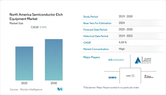
北米の半導体エッチング装置市場は予測期間中にCAGR 4.04%を記録する見込み
主要ハイライト
- 北米の半導体エッチング装置市場の成長は、半導体ウエハーデポジションとウエハープロセスセクターの拡大に依存しています。メモリメーカーや鋳造は、チップ設計コストの上昇、新材料、チップ上の線幅の縮小、製造プロセスの統合の必要性から、より新しく独創的な装置への投資にますます注力しています。例えば、2022年2月、Texas Instrumentsは、2030年まで米国の半導体チップ生産に数十億米ドルを投資する計画を明らかにしました。Texas Instrumentsは、2025年まで米国の半導体チップ製造に年間35億米ドルを投資する計画を明らかにしました。
- 2021年3月、Intelはアリゾナ州にさらに2つの製造工場(ファブ)を新設することを発表しました。このニュースは、世界のチップ不足が自動車から電子機器までの産業を悩ませており、米国が半導体製造に遅れをとっていると懸念されている最中に発表されました。鋳造工場は、モバイル機器に使用されるARM技術による様々なチップを製造する態勢を整えており、歴史的にIntelが支持するx86技術と競合してきました。
- 産業オートメーションと自動車におけるセンサの使用は、半導体のアプリケーションを増加させ、ほぼすべての産業セグメントでの需要が増加しています。このため、半導体エッチング装置市場は間接的に上昇しています。例えば、北アイオワ大学(UNI)、ヤングスタウン州立大学(YSU)、防衛製造加工国立センター(NCDMM)は、初年度の融資で1,000万米ドルの活用を目指す新たな協力関係を結びました。付加製造、人工知能(AI)、ロボット工学などのインダストリー4.0技術導入の障壁を取り除き、サプライチェーンを拡大・強化しながら高品質部品の生産量を増やすことで、毎年数百の企業がパートナーシップの恩恵を受けると期待されています。
- 半導体エッチング装置市場産業は、スマートフォンアプリケーションやその他のコンシューマーアイテムが普及するにつれて成長しています。競争優位を獲得するため、企業はプロセス装置への投資を増やしています。例えば、Intelはオハイオ州の2つの新チップ工場に200億米ドル以上を投資します。この投資により、米国における半導体製造能力は大幅に向上し、コンピューター、スマートフォン、自動車、その他の電子機器の重要なコンポーネントとなります。半導体市場の拡大に伴い、半導体エッチング装置市場も拡大します。
- 半導体エッチング装置産業は多額の資金を必要とし、その開発には政府の支援が不可欠な役割を果たしてきました。市場ベースの政府支援は技術革新と技術普及を促進するかもしれないが、不透明で差別的な補助金は競争を阻害し、市場の歪みを生み出す可能性があります。半導体エッチング装置メーカーに対する偏った政府スキームへの懸念は、メーカーが高品質製品の開発に投資したがらないため、市場開拓を制約しています。
- COVID-19は半導体産業のサプライチェーンと生産を混乱させることで市場に悪影響を与えています。労働力不足のため、半導体エッチング装置メーカーへの影響はより深刻です。世界中の半導体サプライチェーンのいくつかの企業は、パンデミックの間、操業を制限、あるいは停止せざるを得なかった。このセクターは、高額の赤字と需要の増加に悩まされ、その結果、サプライチェーンのギャップがかなり生じた。
北米の半導体エッチング装置市場動向
米国が中国との貿易摩擦を避けるために半導体と周辺製品を製造する戦略が北米市場を牽引しています。
- 国内半導体製造は米国政府の運営に不可欠です。新政権は、増加するチップ不足を解決し、チップ製造のアウトソーシングによって米国がサプライチェーンの途絶に対してより脆弱になったという議員たちの懸念に対処することが期待されています。バイデンは、新たな施策と政府の支援により、米国のチップ企業を大幅に後押しする可能性のある100日間の見直しを開始しました。これにより、北米の半導体エッチング装置市場は成長を続けています。
- 米国のチップ需要の大半は、大型P.C.や情報通信インフラ(データセンターやネットワーク機器を含む)、アプリケーション市場、スマートフォン、産業機器などです。Appleなど米国を拠点とするスマートフォン・メーカーは、TSMCの有力な顧客です。米国政府は、国内のチップ製造を支援するため、500億米ドルの資金拠出を求めています。TSMCは、米国アリゾナ州のチップ工場に、これまで公表していたよりも数百億米ドル多く資金を投入する計画を検討しています。加えて、TSMCは工場建設において、米国政府からの補助金を巡ってIntel社やSamsung Electronicsと競合することが予想されます。これらはすべて、この地域の半導体エッチング装置市場の成長を促す環境を作り出しています。
- 米国の新しい貿易協定は、北米の半導体ビジネスに利益をもたらすもう一つの明確なステップです。米国の国家技術・産業基盤は、日本、韓国、ドイツ、オランダといった、半導体サプライチェーンにおける支配的な参入企業を含む同盟国へと拡大される可能性があります。さらに、米国と欧州連合(EU)間の貿易協定(包括的・先進的TPP(旧TPP)や環大西洋貿易投資パートナーシップなど)は、米国半導体やハイテク機器に対する外国の障壁を低くする一方で、輸入半導体関連商品やサービスへのアクセスを増加させると考えられます。このため、同地域の半導体エッチング装置市場は拡大すると考えられます。
- 米国技術革新競争法(USICA)と政権は、半導体市場への民間投資を促進し、米国の技術的リーダーシップを継続させるために、上下両院と協力して520億米ドルを拠出しています。例えば、S.K.グループによる米国での新しい研究開発センターへの投資や、マイクロンによる米国での生産拡大などです。このため、この地域の半導体エッチング装置市場は増加すると考えられます。
5Gとインダストリー4.0への先端半導体チップの応用が市場成長を促進
- 北米地域の企業は、産業オートメーションへの5G技術の導入に注力しています。例えば、シカゴのDigital Manufacturing InstituteとNational Center for Cybersecurity in Manufacturingは、工場設備の自動化、モニタリング、予知保全を行うためのセンサに接続するプライベート5Gネットワークを設置しました。
- カナダはビジネスに開かれた国として国際的に高い評価を受けています。カナダは、将来の半導体鋳造の展望において著名な地域となるために不可欠な措置を講じる態勢を整えています。加えて、同国は市場において重要なパートナーシップ活動を確認しています。例えば、カナダ政府は1億5,000万カナダドルの半導体チャレンジと、通信ネットワークで使用されるフォトニクス製造センターのためのカナダ国立研究評議会への9,000万カナダドルの支援を開始しました。
- 通信ネットワークのインフラには半導体の用途があります。半導体と半導体エッチング装置の内製化を促進するため、カナダ政府は外国の通信ネットワークインフラプロバイダーの国内での事業を制限しています。例えば、政府はHuaweiやZTEの製品やサービスをカナダの通信システムで使用することを禁止しています。
- Samsung Electronicsはテキサス州テイラーに170億米ドルのチップ製造工場の設立を計画しています。この新しい施設では、モバイル、5G、高性能コンピューティング、人工知能で使用される先進的プロセス技術による製品が生産される予定で、この地域の半導体エッチング装置市場を牽引することになります。
- Lam Research Corporationはアメリカのウエハー製造装置サプライヤーで、5GとWi-Fi 6/6Eを組み合わせたワイヤレス接続性の開発に取り組んでいます。これら2つの技術が同一または近接する周波数帯に存在すると、並列ネットワークの構築が極めて困難になります。同社では現在、窒化アルミニウム膜のスカンジウム・ドーピング・レベルを高め(通常は20%超)、デバイス性能を向上させています。このことは、この地域の半導体エッチング装置市場の急速な技術開拓を示しています。
北米の半導体エッチング装置産業概要
北米の半導体エッチング装置市場は競争が激しく、少数の主要企業が大きな市場シェアを占めています。新規参入者にとって、多額の資本が必要なためこの市場に参入するのは難しく、重要な企業は市場の優位性を拡大するためにM&Aを進めています。
- 2021年9月、Applied Materials, Inc.は、世界有数の炭化ケイ素(Sic)チップメーカーが、ウェハー当たりのダイ生産量をほぼ倍増させる150mmウェハーから200mmウェハー生産へのシフトを支援する新しいソリューションを発表しました。
- 2022年2月、Lam Research Corporation社は、ゲート・オール・アラウンド(GAA)トランジスタ構造の開発でチップメーカーをサポートするために、画期的なウエハー製造技術と新しい化学品を適用した新しい選択的エッチング製品群を発表しました。Argos(R)、Prevos(TM)とSelis(R)エッチポートフォリオなどの3つの製品は、先端ロジックとメモリ半導体ソリューションの設計と製造において強力な優位性を記載しています。
- Panasonic Corporationは2022年2月、独自のロール・ツー・ロール工法により、低抵抗と高トランスミッションを両立した両面フル配線透明導電フィルムを世界で初めて製品化しました。パナソニック独自のロール・ツー・ロール工法により、従来のエッチング工法では不可能であった2mの配線幅を実現しました。
その他の特典
- エクセル形式の市場予測(ME)シート
- 3ヶ月間のアナリストサポート
目次
第1章 イントロダクション
- 調査の成果
- 調査の前提
- 調査範囲
第2章 調査手法
第3章 エグゼクティブサマリー
第4章 市場力学
- 市場概要
- 市場促進要因
- 中国との貿易摩擦を回避するための米国の半導体と周辺製品の内製化戦略
- 5Gとインダストリー4.0における先端半導体チップの用途
- 市場抑制要因
- 透明性が低く、政府による差別的補助金の可能性
- バリューチェーン/サプライチェーン分析
- ポーターのファイブフォース分析
- 新規参入業者の脅威
- 買い手/消費者の交渉力
- 供給企業の交渉力
- 代替品の脅威
- 競争企業間の敵対関係の強さ
- COVID-19が市場に与える影響
第5章 市場セグメンテーション
- 製品タイプ別
- 高密度エッチング装置
- 低密度エッチング装置
- エッチングタイプ別
- 導体エッチング
- 誘電体エッチング
- ポリシリコンエッチング
- 用途別
- ロジックとメモリ
- パワーデバイス
- MEMS
- その他
- 国別
- 米国
- カナダ
第6章 競合情勢
- 企業プロファイル
- Applied Materials, Inc
- Hitachi High Technologies America, Inc
- Lam Research Corporation
- SEMES
- Axcelis Technologies, Inc.
- ASM America
- Lattice Semiconductor Corporation
- Texas Instruments
- Panasonic Corporation
第7章 投資分析
第8章 市場の将来
目次
Product Code: 90874
The North America Semiconductor Etch Equipment Market is expected to register a CAGR of 4.04% during the forecast period.
Key Highlights
- The growth of the semiconductor Etch Equipment market in North America is dependent on the expansion of the semiconductor wafer deposition and wafer processing sectors. Memory makers and foundries are increasingly focusing on investing in newer and creative equipment due to rising chip design costs, new materials, smaller linewidths on a chip, and the necessity for integrated manufacturing processes. For instance, in February 2022, Texas Instruments detailed its plan to invest billions in U.S. semiconductor chip production through 2030. Texas Instruments revealed plans to invest USD 3.5 billion annually in its U.S. semiconductor chip manufacturing through 2025 as manufacturers face a global shortage of the tech necessary for an increasing number of goods.
- In March 2021, Intel committed to two more new fabrication plants, or fabs, in Arizona. The news comes during a global chip shortage that is snarling industries from automobiles to electronics and worries the United States is falling behind in semiconductor manufacturing. The foundry is poised to manufacture a range of chips based on ARM technology used in mobile devices and has historically competed with Intel's favored x86 technology.
- Industrial automation and the usage of sensors in automotive are increasing the applications of semiconductors and their demand in almost all the industry verticals. Because of this, the Semiconductor Etch Equipment market is rising indirectly. For instance, The University of Northern Iowa (UNI), Youngstown State University (YSU), and the National Center for Defense Manufacturing and Machining (NCDMM) have formed new cooperation that aims to leverage $10 million in first-year financing. Hundreds of businesses are expected to benefit from the partnership each year by removing barriers to adopting Industry 4.0 technologies, such as additive manufacturing, artificial intelligence (AI), and robotics, to increase the output of high-quality parts while expanding and strengthening the supply chain.
- The semiconductor Etch Equipment market industry is growing as smartphone applications and other consumer items become more popular. To achieve a competitive advantage, firms increase their investment in process equipment. For example, Intel will invest more than USD 20 billion in two new chip plants in Ohio. This investment will significantly increase semiconductor manufacturing capabilities in the United States, a critical component of computers, smartphones, automobiles, and other electronic devices. With the increase of the semiconductor market, the semiconductor Etch Equipment market will also increase.
- The semiconductor Etch Equipment industry requires a large amount of cash, and government support has played an essential role in its development. While market-based government support may promote innovation and technological diffusion, non-transparent and discriminatory subsidies can stifle competition and generate market distortions. Fears about skewed government schemes for semiconductor etch equipment makers are constraining market expansion since manufacturers are unwilling to invest in developing high-quality products.
- COVID-19 has negatively impacted the market by disrupting the semiconductor industry's supply chain and production. Due to workforce shortages, the impact on semiconductor etches equipment makers were more severe. Several players in the semiconductor supply chain worldwide had to limit or even cease their operations during the pandemic. The sector was plagued by a high deficit and rising demand, resulting in a considerable supply chain gap.
North America Semiconductor Etch Equipment Market Trends
The United States' strategies for manufacturing semiconductors and peripheral products to avoid trade tensions with China are driving the market in North America.
- Domestic semiconductor manufacturing is essential for the administration of the U.S. government. The new administration is expected to fix the rising chip shortages and address lawmakers' concerns that outsourcing chipmaking had made the United States more vulnerable to supply chain disruptions. In an executive action, Biden started a 100-day review that could significantly boost American chip companies with additional new policies and government support. This is increasing the North American semiconductor Etch Equipment market to grow.
- Most demand for chips in the United States includes large P.C.s and information and communications infrastructure (including data centers and network equipment), application markets, smartphones, and industrial equipment. Smartphone manufacturers based out of the United States, such as Apple, are prominent customers of TSMC. The United States government has called for USD 50 billion in funding to support domestic chip manufacturing. TSMC is weighing plans to pump tens of billions of dollars more into the chip factories in the U.S. state of Arizona than it had previously disclosed. In addition, TSMC is expected to compete against Intel Corp and Samsung Electronics Co Ltd for subsidies from the U.S. government in building the plants. These all create a conducive environment for the growth of the semiconductor Etch Equipment market in the region.
- New U.S. trade agreements are another clear step that would benefit the semiconductor business in North America. The United States National Technology and Industrial Base might be expanded to include allies such as Japan, South Korea, Germany, and the Netherlands, dominant players in the semiconductor supply chain. In addition, trade agreements between the United States and the European Union, such as the Comprehensive and Progressive Trans Partnership (formerly the TPP) and the Transatlantic Trade and Investment Partnership, would increase access to imported semiconductor-related goods and services while lowering foreign barriers to U.S. semiconductors and high-tech devices. Because of this, the semiconductor Etch Equipment market in the region will increase.
- The U.S. Innovation and Competition Act (USICA) and the Administration are working with the House and Senate to provide $52 billion to catalyze more private-sector investments in the semiconductor market and continued American technological leadership. For example, S.K. Group investments in a new R&D center in USA and Micron to expand U.S. production. Due to this, the semiconductor Etch Equipment market in the region will increase.
The application of advanced semiconductor chips in 5G and Industry 4.0 is fostering the market growth
- Companies in the North American region are focusing on implementing 5G technology in Industrial Automations. For example, The Digital Manufacturing Institute and the National Center for Cybersecurity in Manufacturing in Chicago have installed a private 5G network with connections to sensors to automate, monitor, and provide predictive maintenance for factory equipment, which will serve as a real-world model for companies investigating the potential benefits of Industry 4.0 technologies and applications.
- Canada has a significant reputation internationally as a country open for business. It is poised to take essential steps to emerge as a prominent region in the future semiconductor foundry landscape. In addition, the country is witnessing significant partnership activities in the market. For instance, the Canadian government has launched a Canadian Dollar 150 million semiconductor challenge and a Canadian Dollar 90 million to the national research council of Canada for photonics fabrication centers used in the telecommunication network.
- There are applications of semiconductors in communication network infrastructure. To encourage the in-house manufacturing of semiconductors and Semiconductor Etch Equipment, the Canadian government has restricted foreign telecommunication network infra providers from operating in the country. For example, the government prohibits Huawei and ZTE goods and services from being used in Canada's telecommunications systems.
- Samsung Electronics plans to set up a USD 17 billion chip fabrication plant in Taylor, Texas. This new facility will produce goods based on sophisticated process technologies for use in mobile, 5G, high-performance computing, and artificial intelligence, which will drive the Semiconductor Etch Equipment market in the region.
- Lam Research Corporation is an American supplier of wafer fabrication equipment and is working on developing wireless connectivity by combining 5G and Wi-Fi 6/6E. These two technologies in the same or nearby frequency bands will make parallel network setup extremely difficult. Higher scandium doping levels (usually >20 percent) in aluminum nitride films are currently being used by the company to improve device performance. This shows the rampant technological development of the region's semiconductor Etch equipment market.
North America Semiconductor Etch Equipment Industry Overview
The North America Semiconductor Etch Equipment Market is competitive, and few key players contribute to the significant market share. For new entrants, it is difficult to enter this market due to the significant capital required, and significant businesses are pursuing mergers and acquisitions to expand their market dominance.
- In September 2021, Applied Materials, Inc. announced new solutions to help the world's leading silicon carbide (Sic) chipmakers shift from 150mm to 200mm wafer production, which nearly doubles die output per wafer, to help meet the world's growing demand for premium electric vehicle powertrains.
- In Feb 2022, Lam Research Corp announced a new suite of selective etch products that apply breakthrough wafer fabrication techniques and novel chemistries to support chipmakers in developing gate-all-around (GAA) transistor structures. The company's three products, such as Argos(R), Prevos(TM), and Selis(R) etch portfolio, provide a powerful advantage in designing and manufacturing advanced logic and memory semiconductor solutions.
- In Feb 2022, Panasonic Corporation commercialized a double-sided full wiring transparent conductive film combining low resistance and high transmissivity, using its unique roll-to-roll construction method for the first time. Panasonic's original roll-to-roll fabrication approach allowed for a wiring width of 2 m, which was impossible to achieve with traditional etching procedures.
Additional Benefits:
- The market estimate (ME) sheet in Excel format
- 3 months of analyst support
TABLE OF CONTENTS
1 INTRODUCTION
- 1.1 Study Deliverables
- 1.2 Study Assumptions
- 1.3 Scope of the Study
2 RESEARCH METHODOLOGY
3 EXECUTIVE SUMMARY
4 MARKET DYNAMICS
- 4.1 Market Overview
- 4.2 Market Drivers
- 4.2.1 The United States' strategies for the manufacturing in-house semiconductors and peripheral products to avoid trade tensions with China
- 4.2.2 The application of advanced semiconductor chips in 5G and Industry 4.0
- 4.3 Market Restraints
- 4.3.1 Non-transparent and chance of Government discriminatory subsidies
- 4.4 Value Chain / Supply Chain Analysis
- 4.5 Porter's Five Forces Analysis
- 4.5.1 Threat of New Entrants
- 4.5.2 Bargaining Power of Buyers/Consumers
- 4.5.3 Bargaining Power of Suppliers
- 4.5.4 Threat of Substitute Products
- 4.5.5 Intensity of Competitive Rivalry
- 4.6 COVID-19 Impact on the Market
5 MARKET SEGMENTATION
- 5.1 By Product Type
- 5.1.1 High-density Etch Equipment
- 5.1.2 Low-density Etch Equipment
- 5.2 By Etching Type
- 5.2.1 Conductor Etching
- 5.2.2 Dielectric Etching
- 5.2.3 Polysilicon Etching
- 5.3 By Application
- 5.3.1 Logic and Memory
- 5.3.2 Power Devices
- 5.3.3 MEMS
- 5.3.4 Others
- 5.4 Country
- 5.4.1 United States
- 5.4.2 Canada
6 COMPETITIVE LANDSCAPE
- 6.1 Company Profiles
- 6.1.1 Applied Materials, Inc
- 6.1.2 Hitachi High Technologies America, Inc
- 6.1.3 Lam Research Corporation
- 6.1.4 SEMES
- 6.1.5 Axcelis Technologies, Inc.
- 6.1.6 ASM America
- 6.1.7 Lattice Semiconductor Corporation
- 6.1.8 Texas Instruments
- 6.1.9 Panasonic Corporation
