
|
市場調査レポート
商品コード
1630165
誘電体エッチングの世界市場:市場シェア分析、産業動向、成長予測(2025~2030年)Global Dielectric Etchers - Market Share Analysis, Industry Trends & Statistics, Growth Forecasts (2025 - 2030) |
||||||
カスタマイズ可能
適宜更新あり
|
|||||||
| 誘電体エッチングの世界市場:市場シェア分析、産業動向、成長予測(2025~2030年) |
|
出版日: 2025年01月05日
発行: Mordor Intelligence
ページ情報: 英文 100 Pages
納期: 2~3営業日
|

全表示
- 概要
- 目次
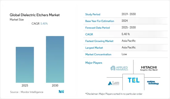
誘電体エッチングの世界市場は予測期間中にCAGR 5.4%を記録する見込み
主なハイライト
- ニューロモルフィックチップ需要の増加がエッチャー市場を牽引人工知能、データ処理、分析に対する需要の高まりは、世界中のニューロモルフィックチップの革新と採用に影響を与える主要因です。エッチング技術は、ウエハー上のコーティングや材料を選択的に除去してチップの特徴を作り出すのに役立ちます。これらの手順は、除去が困難な材料の組み合わせでますます小さく複雑な特徴を作り出すことを必要とします。
- 誘電体エッチングの世界市場の最新動向は、3D ICの出現です。エネルギー消費量の少ない高速コンピューティングデバイスへの需要の高まりが、3Dチップ積層への需要を大きく後押ししています。航空宇宙、自動車、医療などの分野における電子デバイスの小型化ニーズの高まりは、0~10nm、さらには原子レベルの精度で構造を変化させることができる誘電体エッチングの需要を促進します。
- エッチ法はまた、チップ・パッケージングや微小電気機械システム統合(MEMS)を可能にするスルーシリコン・ビア(TSV)のような、高さのある高アスペクト比の特徴も作り出します。例えば、ラムリサーチのプラズマエッチングシステムは、高くて狭いものから、短くて広いもの、数オングストロームの大きさまで、精密な構造を構築するのに必要な高性能と高生産性を提供します。
- アプライドマテリアルズは2021年5月、DRAMの微細化とチップの性能、消費電力、面積、コスト、市場投入期間(PPACt)の最適化を実現する3つの新たな材料エンジニアリングソリューションを発表しました。DRAMメーカーは、アプライドマテリアルズが開発した低誘電率材料であるブラックダイヤモンドを使用して、ロジック配線のスケーラビリティ問題を解決しています。
- COVID-19の発生は、2020年の初期段階においてサプライチェーンと生産を大きく混乱させました。その影響は、半導体エッチング装置の主要エンドユーザーである半導体メーカーにとってより深刻でした。人手不足のため、半導体サプライチェーンの多くのプレーヤーが操業の縮小、あるいは停止を余儀なくされました。業界は高赤字と需要増にさいなまれ、サプライチェーンに大きなギャップが生じた。ウィルスの最初の広がりは、自動車などの主要セクターにおけるチップ需要の減少を恐れ、鋳造工場の操業停止や稼働率低下につながった。生産量の減少は、半導体鋳造による当初の予測にもかかわらず、需要が増加するにつれて世界の半導体不足につながった。
誘電体エッチング市場動向
ニューロモルフィック・チップへの需要が誘電体エッチング市場を押し上げる
- ニューロモルフィック・チップは、生物学的な脳の処理能力にヒントを得たデータ・プロセッサで、高速かつ低消費電力の学習を実現し、数百万個の神経細胞の能力を備えています。このチップのサイズはモバイルに十分なほど小さく、応用範囲は広いです。
- また、AIベースの新興企業は日々増加しています。AIによって可能になる技術は、処理にニューロモルフィック・チップを必要とします。したがって、人工知能、データ処理、分析に対する需要の高まりは、世界中のニューロモルフィックチップの技術革新と採用に影響を与える主要因であり、これが誘電体エッチング市場を牽引すると予想されます。
- 人工知能、データ処理、分析に対する需要の高まりは、世界中でニューロモルフィックチップの採用を促進する重要な要因であり、それによって誘電体エッチングのニーズが生まれます。さらに、高度なインテリジェントデバイスのためのモノのインターネットアプリケーションの急速な技術的アップグレードも、技術的に高度な半導体の需要を押し上げると予測されています。その結果、誘電体エッチングの需要が大幅に増加すると予測されています。
- DRAMは、世界経済のデジタル移行により高い需要があります。モノのインターネットにより、エッジにコンピュータデバイスが大量に追加され、その結果、処理のためにクラウドに転送されるデータが飛躍的に増加します。業界では、DRAMをより高速に動作させ、消費電力を抑えながら、サイズとコストを縮小できるような進歩が求められており、これが市場成長の原動力となっています。
- スマートフォンや、半導体ICを必要とする家庭用電子機器市場のその他のアプリケーションは、誘電体エッチングの需要を促進しています。さらに、モノのインターネット(IoT)デバイスの数が増加するにつれて、半導体業界は、より革新的な製品を製造するためにこの技術に投資することを目指しています。
アジア太平洋地域が大きなシェアを占める
- クアルコム、ブロードコム、エヌビディア、メディアテック、アップル、AMDなど、世界中の集積デバイスメーカー(IDM)はファブレス・ビジネスモデルを採用しています。ファブレス・ビジネスモデルは、売上を維持するために必要な高い生産量を維持しながら、新技術の研究開発に利益を集中投資することを可能にします。
- TSMC、UMC、DB Hitek、SMICなどの組織は、顧客の要求仕様と生産量に応じてチップセットを生産するために鋳造所を利用しています。これらの鋳造所の大部分は、中国、台湾、韓国で操業しています。
- 原子層エッチング(ALE)は、浅い構造で優れた深さ制御を提供する洗練されたエッチングプロセスです。デバイスのフィーチャーサイズが小さくなるにつれ、性能向上に必要な精度を達成するためにALEの必要性が高まっています。
- 最先端のマイクロエレクトロニクスデバイスの製造には、高忠実度のパターン転写(エッチング)が必要です。フィーチャーが10nm以下のサイズに縮小し、新しいデバイスが極薄の2D材料を使用するようになると、原子レベルの精度がより重要になります。このため、従来の(連続)エッチングの限界を原子レベルで克服する技術である原子層エッチング(ALE)の需要が高まった。
- TSMCはアップルのAシリーズチップの独占製造メーカーとなっています。このチップセットは、A13と呼ばれる7ナノメーターのチップセットを使用して製造されます。また、アジア太平洋地域では自動車エレクトロニクス産業が非常に盛んであり、市場成長の機会が豊富にあります。
誘電体エッチング産業の概要
誘電体エッチングの世界市場は非常に競争が激しいです。大小さまざまな企業が存在するため、市場は非常に集中しています。大手企業はいずれも市場で大きなシェアを占めており、世界中の消費者基盤の拡大に注力しています。同市場における主要企業には、 Applied Materials Inc., Hitachi High-Technologies Corporation, Lam Research Corporation, Tokyo Electron, Mattson Technology, Inc., Advanced Micro-Fabrication Equipment Inc.などが挙げられます。各社は、予測期間中に競争力を獲得するため、複数のパートナーシップを結び、新製品の投入に投資することで市場シェアを拡大しています。
- 2022年7月- 東京エレクトロンとIBMは、ガラスウエハーベースの必要性をなくし、プロセスを合理化する最新のフロント3Dチップ積層で協業。IBMと東京エレクトロンは、3Dチップ製造用のシリコンキャリアウエハを欠点なしに実現する方法を発見しました。このプロセスは、新しい300mmモジュールを使って実証されたもので、両社によれば、300mmレベルの3D積層シリコン・チップ・ウェーハはこれが初めてだといいます。IBMは、3Dチップ積層技術への多大な投資が半導体の生産プロセスを合理化し、世界のチップ不足に一筋の光明をもたらすことを期待しています。
- 2022年6月-ラムリサーチはSKハイニックスと協力し、ドライレジスト極端紫外線技術でDRAMの生産コスト効率を高める。ラムの革新的なドライレジスト製造技術は、先進的なDRAMチップを製造するための2つの重要なプロセス工程の開発ツールです。LAMが2020年に導入したこのドライレジスト技術は、次世代半導体の製造において極めて重要な技術であるEUV(極端紫外線)リソグラフィーの歩留まり、解像度、生産性、および生産性を向上させます。材料レベルでは、ラムのドライレジスト技術はEUVリソグラフィの最大の課題に対処し、高度なメモリとロジックのためのコスト効率の高いスケーリングを可能にします。
その他の特典:
- エクセル形式の市場予測(ME)シート
- 3ヶ月間のアナリスト・サポート
目次
第1章 イントロダクション
- 調査の前提条件と市場定義
- 調査範囲
第2章 調査手法
第3章 エグゼクティブサマリー
第4章 市場洞察
- 市場概要
- 業界の魅力度-ポーターのファイブフォース分析
- 供給企業の交渉力
- 消費者の交渉力
- 新規参入業者の脅威
- 代替品の脅威
- 競争企業間の敵対関係の強さ
- COVID-19の市場への影響
第5章 市場力学
- 市場促進要因
- ニューロモルフィックチップの世界需要
- 3D ICの出現
- 電子デバイスの小型化
- 市場の課題/抑制要因
- 初期コストの上昇
第6章 市場セグメンテーション
- タイプ別
- ウェットエッチング
- ドライエッチング
- 原子レベルエッチング(ALE)
- 地域別
- 北米
- 欧州
- アジア太平洋
- その他の地域
第7章 競合情勢
- 企業プロファイル
- Applied Materials, Inc.
- Hitachi High-Technologies Corporation
- Lam Research Corporation
- Tokyo Electron Limited
- Mattson Technology
- Advanced Micro-Fabrication Equipment Inc.
- Jusung Engineering
- Oxford Instruments
- SEMES Co. Ltd.
- ULVAC, Inc.
第8章 投資分析
第9章 市場の将来
The Global Dielectric Etchers Market is expected to register a CAGR of 5.4% during the forecast period.
Key Highlights
- An increase in demand for neuromorphic chips will drive the market for etchers. The rising demand for artificial intelligence, data processing & analytics is a major factor influencing the innovation & adoption of neuromorphic chips across the globe. Etch techniques aid in creating chip features by eliminating coatings and materials put on the wafer selectively. These procedures entail producing increasingly small and intricate features with difficult-to-remove material combinations.
- The latest trend in the global dielectric etchers market is the emergence of 3D ICs. With the increasing demand for faster computing devices that consume less amount of energy will significantly drive the demand for 3D chip stacking. The growing need for miniaturizing electronic devices in fields such as Aerospace, Automotive & Medical sectors will drive the demand for dielectric etchers, which are capable of altering structures to a precision of 0 - 10 nm & even at an atomic level.
- Etch methods also produce tall, high-aspect-ratio features, like through-silicon vias (TSVs), which allow chip packaging and micro-electromechanical system integration (MEMS). For instance, Lam Research plasma etch systems provide high-performance and high-productivity capabilities required to build precise structures, ranging from tall and narrow, short and wide, to a few angstroms in size.
- In May 2021, Applied Materials, Inc. announced three new materials engineering solutions that enable its memory customers three new options to scale DRAM and optimize chip performance, power, area, cost, and time to market (PPACt). DRAM manufacturers use black diamond, a low-k dielectric material developed by Applied Materials, to solve logic interconnect scalability problems.
- The outbreak of COVID-19 significantly disrupted the supply chain and production during the initial phase of 2020. The impact was more severe for semiconductor manufacturers, the major end users for semiconductor etch equipment. Due to labor shortages, many players in the semiconductor supply chain had to reduce or even suspend their operations. The industry was riddled with a high deficit and increasing demand, which led to a significant supply chain gap. The initial spread of the virus led to the shutting down or reduction of foundry capacity utilization, fearing the decreasing demand for chips across major sectors, like the automotive. Diminished output led to a global shortage of semiconductors as demand increased, despite the initial estimates by semiconductor foundries.
Dielectric Etchers Market Trends
Demand for Neuromorphic Chip to Boost Dielectric Etchers Market
- A neuromorphic chip is a data processor inspired by biological brain processing ability to achieve high-speed & low power learning and constructed with capabilities of millions of neurons. The size of these chips is small enough to go mobile, and applications are broad.
- Besides, AI-based startups are increasing day by day. The technologies enabled by AI require neuromorphic chips for processing. Therefore, the rising demand for artificial intelligence, data processing & analytics is a major factor influencing the innovation & adoption of neuromorphic chips across the globe, which in turn is expected to drive the market for dielectric etchers.
- The rising demand for artificial intelligence, data processing, and analytics is a significant factor that drives the adoption of neuromorphic chips worldwide, thereby creating the need for dielectric etchers. Moreover, rapid technological upgradation of Internet of Things applications for advanced intelligent devices is also anticipated to boost the demand for technologically advanced semiconductors. This, in turn, is predicted to create significant demand for dielectric etching in the market.
- DRAM is in high demand due to the global economy's digital transition. The Internet of Things creates significant additional computer devices at the edge, resulting in an exponential rise in data that is transported to the cloud for processing. The industry needs advancements that would allow DRAM to scale down in size and cost while running at greater speeds and consuming less power, which drives the market growth.
- Smartphones and other applications in the consumer electronics market that require semiconductor ICs drive the demand for dielectric etcher. Furthermore, as the number of Internet of Things (IoT) devices grows, the semiconductor industry aims to invest in this technology to produce more innovative products.
Asia Pacific Region to Hold a Significant Share
- Integrated Device Manufacturers (IDM) such as Qualcomm, Broadcom Ltd., Nvidia, MediaTek, Apple, AMD, etc. across the globe are adopting fabless business model, where the organization will design the chipset layout and outsource the manufacturing to chipset manufacturers such as TSMC, UMC & SMIC. The fabless business model helps organizations to concentrate their efforts on investing profits in research and development of new technologies while maintaining the high production volumes needed to maintain sales.
- Organizations such as TSMC, UMC, DB Hitek, SMIC, etc. utilize their foundries to produce the chipset according to the specifications and volumes requirement of the customers. A major share of these foundries operates from China, Taiwan & South Korea.
- Atomic layer etching (ALE) is a sophisticated etching process that provides superior depth control on shallow structures. As device feature size shrinks, ALE becomes increasingly necessary to attain the accuracy required for enhanced performance.
- The production of advanced microelectronic devices requires high-fidelity pattern transfer (etching). As features drop to sub-10nm sizes and new devices use ultra-thin 2D materials, atomic-scale accuracy becomes more important. This raised the demand for atomic layer etching (ALE), a technique that overcomes the limits of traditional (continuous) etching at the atomic level.
- TSMC has been Apple's exclusive manufacturer of Apple's A-series chips. This chipset will be fabricated using a 7-nanometer chipset called A13. Besides, with automotive electronics industry flourishing exceedingly in the region, Asia-Pacific is providing a plethora of opportunities for market growth.
Dielectric Etchers Industry Overview
The Gloabl Dielectric Etchers Market is very competitive in nature. The market is highly concentrated due to the presence of various small and large players. All the major players account for a large share of the market and are focusing on expanding their consumer base across the world. Some of the significant players in the market are Applied Materials Inc., Hitachi High-Technologies Corporation, Lam Research Corporation, Tokyo Electron, Mattson Technology, Inc., Advanced Micro-Fabrication Equipment Inc., and many more. The companies are increasing the market share by forming multiple partnerships and investing in introducing new products to earn a competitive edge during the forecast period.
- July 2022 - Tokyo Electron and IBM collaborated for the latest front 3D chip stacking that removes the need for a glass wafer base, streamlining the process. IBM and Tokyo Electron, however, have found a way to enable silicon carrier wafers for 3D chipmaking without the drawbacks. This process was demonstrated using a new 300mm module, which the companies say is the first 3D stacked silicon chip wafer at the 300mm level. IBM hopes that the considerable investments in 3D chip stacking technology can help streamline the production process of semiconductors and offer a silver lining to the global chip shortage.
- June 2022 - Lam Research collaborated with SK Hynix to enhance DRAM production cost efficiency with dry resist Extreme Ultraviolet technology. Lam's innovative dry resist fabrication technology is a development tool for two key process steps for producing advanced DRAM chips. This technology introduced by LAM in 2020, dry resist, extends the yield, resolution, productivity, and of EUV (Extreme Ultraviolet) lithography, a pivotal technology in producing next-generation semiconductors. At the material level, Lam's dry resist technology addresses EUV lithography's biggest challenges, enabling cost-effective scaling for advanced memory and logic.
Additional Benefits:
- The market estimate (ME) sheet in Excel format
- 3 months of analyst support
TABLE OF CONTENTS
1 INTRODUCTION
- 1.1 Study Assumptions and Market Definition
- 1.2 Scope of the Study
2 RESEARCH METHODOLOGY
3 EXECUTIVE SUMMARY
4 MARKET INSIGHTS
- 4.1 Market Overview
- 4.2 Industry Attractiveness - Porter's Five Forces Analysis
- 4.2.1 Bargaining Power of Suppliers
- 4.2.2 Bargaining Power of Consumers
- 4.2.3 Threat of New Entrants
- 4.2.4 Threat of Substitutes
- 4.2.5 Intensity of Competitive Rivalry
- 4.3 Impact of COVID-19 on the Market
5 MARKET DYNAMICS
- 5.1 Market Drivers
- 5.1.1 Global Demand of Neuromorphic Chip
- 5.1.2 Emergence of 3D ICs
- 5.1.3 Miniaturizing Electronic Devices
- 5.2 Market Challenge/Restraint
- 5.2.1 Higher Initial Costs
6 MARKET SEGMENTATION
- 6.1 By Type
- 6.1.1 Wet Etching
- 6.1.2 Dry Etching
- 6.1.3 Atomic Level Etching (ALE)
- 6.2 By Geography
- 6.2.1 North America
- 6.2.2 Europe
- 6.2.3 Asia Pacific
- 6.2.4 Rest of the World
7 COMPETITIVE LANDSCAPE
- 7.1 Company Profiles
- 7.1.1 Applied Materials, Inc.
- 7.1.2 Hitachi High-Technologies Corporation
- 7.1.3 Lam Research Corporation
- 7.1.4 Tokyo Electron Limited
- 7.1.5 Mattson Technology
- 7.1.6 Advanced Micro-Fabrication Equipment Inc.
- 7.1.7 Jusung Engineering
- 7.1.8 Oxford Instruments
- 7.1.9 SEMES Co. Ltd.
- 7.1.10 ULVAC, Inc.

