
EUVリソグラフィ:市場シェア分析、産業動向・統計、成長予測(2025年~2030年)
EUV Lithography - Market Share Analysis, Industry Trends & Statistics, Growth Forecasts (2025 - 2030)- 発行日
- ページ情報
- 英文 120 Pages
- 納期
- 2~3営業日
- 商品コード
- 1690153
- カスタマイズ可能 お客様のご希望に応じて、既存データの加工や未掲載情報(例:国別セグメント)の追加などの対応が可能です。詳細はお問い合わせください。
- 適宜更新あり 本レポートは最新情報反映のため適宜更新し、内容構成変更を行う場合があります。ご検討の際はお問い合わせください。
- 翻訳ツール提供対象 PDF対応AI翻訳ツールの無料貸し出しサービスのご利用が可能です
概要
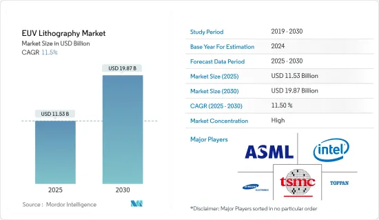
EUVリソグラフィ市場規模は、2025年に115億3,000万米ドルと推定され、2030年には198億7,000万米ドルに達すると予測され、予測期間中(2025年~2030年)のCAGRは11.5%です。
EUVリソグラフィは、波長わずか13.5nmの光を使用します。これは、先端チップ製造における他のリソグラフィ技術、193nmの光を使用するディープ・ウルトラバイオレット・リソグラフィの波長のほぼ14分の1に短縮されます。この技術により、ノードサイズ7nm、あるいは5nm程度の小さなトランジスタ・スケールで、より精密かつ効率的な半導体の生産が可能になります。
主なハイライト
- 半導体の微細化が進む中、EUVリソグラフィ技術の採用は非常に重要になっています。EUVリソグラフィ技術は、5G、AI、自動車などの次世代アプリケーションに最適かつ効率的な選択肢を提供することで、ウエハー上の複雑なパターンの微細化を可能にするからです。EUV技術では、EUV光の波長が短いため、高度な技術に関連する設計のナノメートルスケールの特徴を印刷することが可能であり、チップメーカーはチップの微細化を推進し続けることができます。
- TSMCの極端紫外線(EUV)ツールは生産成熟期に達する見込みで、ツールの稼働率はすでに大量生産の目標値に達しており、日常的な運用では250ワットを超える出力が得られます。チップメーカーは、最先端のロジックを実現するために、7nm、5nm、そしてそれ以降のEUVに期待を寄せており、今日、他に利用可能な選択肢はないです。次世代リソグラフィ技術は準備が整っておらず、7nmと5nmのスケールでは適用できません。3nm以降では、チップメーカーは高NA EUVの使用を望んでいるが、この技術の開発にはまだいくつかの課題があります。
- TSMCもまた、2022年までに3nm製品の量産を開始することを計画しています。市場のもう1つの主要企業であるサムスン電子は、極端紫外線(EUV)リソグラフィ技術で2030年までにTSMCを追い抜くことを目指しています。TSMCは以前、2019年12月に、2020年前半に5nmプロセスベースのチップ供給を開始し、2022年に3nmプロセスチップの量産を開始すると発表しました。また、2024年までに2nmプロセス製品の生産を見込んでいます。
- ASMLはCOVID-19により装置の輸出が困難になり、サムスン電子やTSMCなど世界の主要半導体メーカーに悪影響を与えました。同社の装置納入の遅れにより、両社は戦略的開発と生産ロードマップの変更を余儀なくされています。同社の装置納入の遅れにより、両社は戦略的な開発・生産計画の変更を余儀なくされています。TSMCは3-nm半導体の試験生産を延期しました。一方、サムスン電子は、2020年に5nm半導体の商業生産を開始する予定であったが、2021年後半まで開始できませんでした。
EUVリソグラフィ市場の動向
鋳造メーカーが大きなシェアを占める見込み
- TSMCは、2022年に3nm製品の量産を開始することで、世界のファウンドリ市場を独占する計画です。同市場で後塵を拝しているサムスン電子は、極端紫外線(EUV)リソグラフィ技術で2030年にTSMCを追い抜くことを目指しています。TSMCは2019年12月、2020年前半に5nmプロセスベースのチップ供給を開始し、2022年に3nmプロセスチップの量産を開始すると発表しました。また、2024年には2nmプロセス製品の生産を見込んでいます。
- サムスンは市場で一連の課題に直面しています。例えば、EUVリソグラフィ用フォトレジストの供給は、日本の輸出規制の対象となる可能性があります。その上、相当数の企業がサムスン電子と競合しようとしています。中国と台湾の半導体企業はますます協力関係を深めています。サムスン電子はFinFET、ゲートオールアラウンド、マルチブリッジチャンネルFETなどの新しい微細加工技術を次々と発表し、増え続ける競合他社に対抗しています。
- 2021年2月、サムスン鋳造は米国での最先端半導体製造施設の建設を求め、アリゾナ州、ニューヨーク州、テキサス州の当局に書類を提出しました。テキサス州オースティン近郊に建設予定の工場は、170億米ドルを超える建設費と1,800人の雇用創出が見込まれています。すべてが計画通りに進めば、この鋳造工場は2023年第4四半期までに稼働する予定です。同社はどのプロセス・ノード向けに設計されるのか明言しなかったが、この新ファブには興味をそそられます。
- 台湾セミコンダクター・マニュファクチャリング社(TSMC)やユナイテッド・マイクロエレクトロニクス社(UMC)などのベンダーは、フォルクスワーゲンやトヨタなどの自動車メーカーの需要に応えるため、生産移転に注力していると発表しました。加えて、QualcommやAppleなどの企業からの需要が半導体の供給に遅れをもたらしています。オートモーティブ・ニュースの新しい調査(2021年4月)によると、回答者の53%がチップを米国外から調達していることを示唆し、メーカーの55%が国外で代替のチップ調達先を探しています。
- このような要因が、調査対象市場への新規企業の参入につながっています。例えば、インテルは最近、自動車メーカーの需要に対応するため、新事業インテル鋳造サービスの立ち上げを発表しました。同様に、2021年3月、世界鋳造は、フォード、フォルクスワーゲン、ゼネラルモーターズなどの自動車メーカーの減産を支援するために、世界各地で生産能力拡張のために14億米ドルを投資する予定であると発表しました。
アジア太平洋が大きなシェアを占める見込み
- 極端紫外線(EUV)リソグラフィの世界市場では、アジア太平洋が引き続き最大の売上シェアを占めています。予測期間中、この地域では台湾が優位に立つと予想されます。台湾におけるTSMCの事業拡大とEUVリソグラフィ技術への投資の増加は、台湾の極端紫外線リソグラフィ市場の成長を支える最も重要な要因の一つです。台湾は、アジア太平洋のEUVリソグラフィ市場の大半の収益シェアを占めています。台湾以外では、日本、中国、韓国の極端紫外線リソグラフィ市場が、今後数年間で利害関係者に大きな機会をもたらすと期待されています。
- 米国と中国の貿易摩擦が激化する中、中国の半導体メーカーも自国製品の生産を急ぐため、中古のチップ製造装置を活用しており、日本の中古市場での装置価格を押し上げています。日本の中古装置販売業者によると、価格は昨年より20%上昇しているといいます。旧世代の機械は米国による対中制裁の制限を受けないため、中国のプレーヤーは自由にアクセスできます。
- コロナウィルスの大流行による引きこもり傾向も一因です。世界的にチップ需要が高まる中、最新型でない機器も飛ぶように売れています。その結果、自動車に使われる半導体の供給不足が長期化する可能性もあります。
- ASMLの新しい研修施設は、おそらく両社にとって有益と思われます。同社は欧州最大の半導体機械ブランドだが、台湾メーカーは最大の顧客です。Asian Nikkei Reviewによると、ASMLが今年出荷を予定している35台のEUVシステムのうち20台がTSMC向けだといいます。オランダのASMLは、チップメーカーの従業員により多くのツールを使いこなすことで、将来の販売を準備しています。ASMLはまた、台湾に新たな研究開発施設を開設する予定であり、2023年までに現地従業員数が500人を超えることになります。
EUVリソグラフィ業界の概要
EUVリソグラフィ市場は、ASMLが極端紫外線を使用するリソグラフィ装置の唯一のメーカーであるため、高度に統合されています。同社は、インテル、サムスン、台湾積体電路製造(TSMC)など、世界の半導体ファブリケーターに装置を製造・販売しています。同社の企業収益のほぼ25%はEUV露光装置の販売によるものであり、これはEUV露光装置の製造と商業化における同社の独占を反映しています。
- 2021年12月欧州の注目株であるASMLは、極端紫外線リソグラフィ装置の新バージョンの開発に取り組んでいます。この装置は、世界で最も洗練されたプロセッサーを製造するシリコンの塊にパターンを刻むために使用されます。サムスン、TSMC、インテルは、同社の現在のEUV装置を使用して、次世代のコンピューターやスマートフォン用のチップを製造しています。
- 2021年3月サムスンは、世界最大の鋳造工場であるTSMCに対抗するため、EUVスキャナーを増産します。EUVスキャナーは、従来の装置とは異なり、より微細な回路を生成するために必要なフォトリソグラフィ工程の数を減らすことでチップ製造工程を合理化できる可能性があり、大手チップメーカーがこの技術をめぐって競争する原因となります。
その他の特典:
- エクセル形式の市場予測(ME)シート
- 3ヶ月間のアナリスト・サポート
目次
第1章 イントロダクション
- 調査の前提条件と市場定義
- 調査範囲
第2章 調査手法
第3章 エグゼクティブサマリー
第4章 市場洞察
- 市場概要
- 産業バリューチェーン分析
- 業界の魅力度-ポーターのファイブフォース分析
- 供給企業の交渉力
- 買い手の交渉力
- 新規参入業者の脅威
- 代替品の脅威
- 競争企業間の敵対関係の強さ
- COVID-19の業界への影響評価
第5章 市場力学
- 市場促進要因
- 他と比べてマイクロチップの生産速度が速くなる技術
- チップメーカーによる効率向上のための製造工程削減
- 市場抑制要因
- 既存のDeep UVレーザーからEUVレーザーへの置き換えに伴う高コスト
- 市場内の独占
- 技術スナップショット
第6章 市場セグメンテーション
- 製品タイプ
- 光源
- ミラー
- マスク
- タイプ
- 鋳造
- 集積デバイスメーカー(IDM)
- 地域
- 韓国
- 台湾
- その他
第7章 競合情勢
- 企業プロファイル
- ASML Holding NV
- NTT Advanced Technology Corporation
- Canon Inc.
- Nikon Corporation
- Intel Corporation
- Taiwan Semiconductor Manufacturing Company Limited
- Samsung Electronics Co. Ltd
- Toppan Photomasks Inc.
- Ushio, Inc.
第8章 投資分析
第9章 市場の将来
目次
The EUV Lithography Market size is estimated at USD 11.53 billion in 2025, and is expected to reach USD 19.87 billion by 2030, at a CAGR of 11.5% during the forecast period (2025-2030).
EUV lithography makes the usage of light with a wavelength of just 13.5 nm, which is a reduction of almost 14 times the wavelength of the other lithography techniques in advanced chipmaking, Deep Ultraviolet lithography, which uses 193 nm light. ASML, which is the dominant player in the market, has been exploring ways to reduce transistor sizes and has made considerable strides in the field of EUV lithography, which enables more precise and efficient production of semiconductors at small transistor scales around 7nm node size or even 5nm.
Key Highlights
- As semiconductor geometries tend to grow smaller and smaller, the adoption of EUV lithography technology has become extremely important, as it enables scaling down of intricate patterns on wafers by providing an optimal and efficient choice for next-generation applications, including 5G, AI, and Automotive. EUV technology allows the chip makers to keep driving chip scaling as the shorter wavelength of EUV light is capable of printing the nanometer-scale features of the designs related to the advanced techniques.
- TSMC's Extreme Ultraviolet (EUV) tools are expected to reach production maturity, with tool availability already reaching target goals for high-volume production and output power of greater than 250 watts for daily operations. Chipmakers are banking on EUV at 7nm, 5nm, and beyond for leading-edge logic, and today there are no other options available. The next-generation lithography technologies are not ready and can not be applied at 7nm and 5nm scales. At 3nm and beyond, chipmakers hope to use high-NA EUV, but several challenges have yet to be overcome in developing this technology.
- TSMC has also been planning to start the volume production of the 3-nm products by 2022. Samsung Electronics Co. Ltd, another major player in the market, aims to overtake TSMC by 2030 with its extreme ultraviolet (EUV) lithography technology. TSMC, previously in Dec 2019, announced that the company would be starting to supply 5 Nm process-based chips in the first half of 2020 and will be starting mass production of 3-nm process chips in 2022. The company also anticipates producing 2-nm process products by 2024.
- ASML faced difficulty exporting its equipment due to COVID-19, negatively affecting major global semiconductor producers, including Samsung Electronics and TSMC. A delay in the company's equipment delivery is forcing the two companies to change their strategic development and production roadmaps. Due to a delay in the delivery of the company's equipment, the two companies have to alter their strategic development and production plans. TSMC has postponed the test production of 3-nm semiconductors. Samsung Electronics, meantime, had hoped to commence commercial production of 5-nm semiconductors in 2020 but was unable to do so until late 2021.
EUV Lithography Market Trends
Foundry is Expected to Hold Major Share
- TSMC is planning to dominate the global foundry market by starting the volume production of 3-nm products in 2022. Samsung Electronics Co, Ltd, the runner-up in the market, is aiming to overtake TSMC in 2030 with its extreme ultraviolet (EUV) lithography technology. TSMC announced in December 2019 that the company would start to supply 5-nm process-based chips in the first half of 2020 and start the mass production of 3-nm process chips in 2022. The company also expects o produce 2-nm process products in 2024.
- Samsung is facing a series of challenges in the market. For instance, the supply of photoresists for EUV lithography purposes can be subject to Japan's export restrictions. Besides, a significant number of companies are trying to compete with Samsung Electronics. Chinese and Taiwanese semiconductor companies are increasingly collaborating. Samsung Electronics has unveiled a series of new microfabrication techniques such as FinFET, gate-all-around, and multi-bridge-channel FET to compete with the increasing competitors.
- In February 2021, Samsung Foundry filed documents with authorities in Arizona, New York, and Texas seeking to build a leading-edge semiconductor manufacturing facility in the United States. The potential fab near Austin, Texas, is expected to cost over USD 17 billion and create 1,800 jobs. If everything goes as planned, the foundry will go online by the fourth quarter of 2023. There is an intrigue about the new fab, though the company did not state which process node it will be designed for.
- Vendors, such as Taiwan Semiconductor Manufacturing Co. (TSMC) and United Microelectronics Corp. (UMC), announced that they have been focusing on relocating their production to meet the demand from automakers, such as Volkswagen and Toyota, among others. In addition, the demand coming from companies, such as Qualcomm and Apple, has been creating delays in the supply of semiconductors. According to a new survey by Automotive News (April 2021), 53% of the respondents suggested that they source their chips from outside the United States, and 55% of the manufacturers have been looking for alternative chip sources outside the country.
- Such factors have been leading to the entry of new companies into the market studied. For instance, recently, Intel announced the launch of a new business Intel Foundry Services, to meet the demand for automotive manufacturers. Similarly, in March 2021, Global Foundries announced that it has been planning to invest USD 1.4 billion for capacity expansion in different parts of the world to support automakers cutting output, such as Ford, Volkswagen, and General Motors.
Asia Pacific is Expected to Hold Major Share
- The Asia Pacific continues to hold the largest revenue share in the global market for Extreme Ultraviolet (EUV) lithography. Taiwan is expected to have an edge in the region over the forecast period. TSMC's expansion in Taiwan and its increasing investments in the EUV lithography technology is among the most critical factors instrumental in the growth of the Extreme Ultraviolet lithography market in Taiwan. The country accounts for the majority revenue share of the market for EUV lithography in the Asia Pacific region. Apart from Taiwan, the Extreme Ultraviolet lithography markets in Japan, China, and South Korea are expected to create significant opportunities for stakeholders in the coming years.
- Chinese semiconductor makers are also utilizing used chipmaking machines as they rush to produce homegrown products amid US-Sino trade tensions, driving up equipment prices in Japan's secondary market. Japanese used equipment dealers say prices are up by 20% from last year. Older-generation machines are not restricted by the United States sanctions on China, giving Chinese players unfettered access.
- The stay-at-home trend spurred by the coronavirus pandemic is also a factor. As chip demand rises worldwide, even equipment that is not the most up-to-date is selling at a brisk pace. This, in turn, could prolong the shortage of semiconductors used in automobiles.
- ASML's new training complex will likely be beneficial to both companies. While the firm is Europe's largest semiconductor machinery brand, the Taiwanese manufacturer is its biggest customer. Asian Nikkei Review states that 20 of the 35 EUV systems ASML intends to ship this year are going to TSMC. The Dutch concern is setting up future sales by familiarizing more of the chipmaker's staff with its tools. ASML also plans on opening a new research and development facility in Taiwan, which will bring its local headcount over 500 by 2023.
EUV Lithography Industry Overview
The Extreme Ultraviolet Lithography Market is highly consolidated as ASML is the only manufacturer of lithography machines that use extreme ultraviolet light. The company manufactures and sells its tools to some global semiconductor fabricators, including Intel, Samsung, and Taiwan Semiconductor Manufacturing Company (TSMC). Almost 25% of the company's revenues are generated by sales of EUV lithography systems, which reflects the company's monopoly in the manufacturing and commercialization of EUV lithography systems.
- December 2021: ASML, a hot stock in Europe, is working on a new version of their extreme ultraviolet lithography equipment, which is used to carve patterns into chunks of silicon that produce the world's most sophisticated processors. Samsung, TSMC, and Intel use the company's current EUV equipment to create chips for the next generation of computers and smartphones.
- March 2021: Samsung is increasing its EUV scanner production to compete with TSMC, the world's largest foundry. EUV scanners, unlike traditional machines, may streamline the chip fabrication process by lowering the number of photolithography procedures necessary to generate finer circuits, causing major chipmakers to compete for the technology.
Additional Benefits:
- The market estimate (ME) sheet in Excel format
- 3 months of analyst support
TABLE OF CONTENTS
1 INTRODUCTION
- 1.1 Study Assumptions and Market Definition
- 1.2 Scope of the Study
2 RESEARCH METHODOLOGY
3 EXECUTIVE SUMMARY
4 MARKET INSIGHTS
- 4.1 Market Overview
- 4.2 Industry Value Chain Analysis
- 4.3 Industry Attractiveness - Porter's Five Forces Analysis
- 4.3.1 Bargaining Power of Suppliers
- 4.3.2 Bargaining Power of Buyers
- 4.3.3 Threat of New Entrants
- 4.3.4 Threat of Substitute Products
- 4.3.5 Intensity of Competitive Rivalry
- 4.4 Assessment of COVID-19 Impact on the Industry
5 MARKET DYNAMICS
- 5.1 Market Drivers
- 5.1.1 The technology resulting in a faster output of microchips compared to others
- 5.1.2 Chip makers reducing the manufacturing process for better efficiency
- 5.2 Market Restraints
- 5.2.1 High cost involved in replacing the existing Deep UV with EUV lasers
- 5.2.2 Monopoly existing within the market
- 5.3 Technology Snapshot
6 MARKET SEGMENTATION
- 6.1 Product Type
- 6.1.1 Light Sources
- 6.1.2 Mirrors
- 6.1.3 Masks
- 6.2 Type
- 6.2.1 Foundry
- 6.2.2 Integrated Device Manufacturers (IDMs)
- 6.3 Geography
- 6.3.1 South Korea
- 6.3.2 Taiwan
- 6.3.3 Others
7 COMPETITIVE LANDSCAPE
- 7.1 Company Profiles
- 7.1.1 ASML Holding NV
- 7.1.2 NTT Advanced Technology Corporation
- 7.1.3 Canon Inc.
- 7.1.4 Nikon Corporation
- 7.1.5 Intel Corporation
- 7.1.6 Taiwan Semiconductor Manufacturing Company Limited
- 7.1.7 Samsung Electronics Co. Ltd
- 7.1.8 Toppan Photomasks Inc.
- 7.1.9 Ushio, Inc.
8 INVESTMENT ANALYSIS
9 FUTURE OF THE MARKET
- 発行日
- 発行
- Mordor Intelligence
- ページ情報
- 英文 120 Pages
- 納期
- 2~3営業日