
レーザーリソグラフィ装置の市場機会、成長促進要因、産業動向分析、2025年~2034年予測
Laser Lithography Systems Market Opportunity, Growth Drivers, Industry Trend Analysis, and Forecast 2025 - 2034- 発行日
- ページ情報
- 英文 190 Pages
- 納期
- 2~3営業日
- 商品コード
- 1740912
- カスタマイズ可能 お客様のご希望に応じて、既存データの加工や未掲載情報(例:国別セグメント)の追加などの対応が可能です。詳細はお問い合わせください。
- 翻訳ツール提供対象 PDF対応AI翻訳ツールの無料貸し出しサービスのご利用が可能です
概要
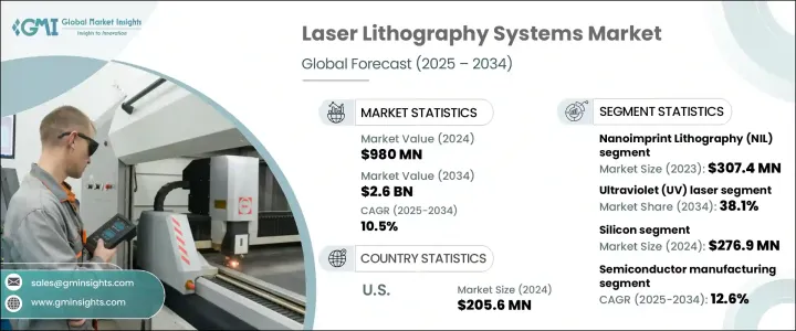
レーザーリソグラフィ装置の世界市場規模は2024年に9億8,000万米ドルとなり、2034年にはCAGR 10.5%で成長し26億米ドルに達すると推定されています。
半導体技術の進歩が小型化と性能の限界を押し広げるにつれて、市場は大きな勢いを増しています。チップメーカーがより小さなノードを積極的に追求する中、レーザーリソグラフィ装置、特に深紫外(DUV)と極端紫外(EUV)システムの役割は、次世代生産に必要な精度とスケーラビリティを提供するために不可欠となっています。人工知能、通信、高性能コンシューマーエレクトロニクスなど、10nm以下の技術へのシフトが進む中、超精密パターニングソリューションの必要性が浮き彫りになっています。
ムーアの法則がメーカーに技術革新を迫り続ける中、レーザーリソグラフィーは、複雑で高密度なデバイスを大規模に生産するための技術的バックボーンを提供しています。研究開発への投資、5Gインフラの採用増加、IoTの拡大、主流アプリケーションへのフォトニクスの統合の増加は、市場の見通しをさらに強化します。チップ製造における持続可能性とエネルギー効率の重視の高まりも、高度なリソグラフィ・ソリューションに有利であり、従来の方法から、より高いスループット、より低い欠陥率、より優れた材料利用を提供するレーザーベースのシステムへの顕著なシフトを推進しています。
| 市場範囲 | |
|---|---|
| 開始年 | 2024 |
| 予測年 | 2025-2034 |
| 開始金額 | 9億8,000万米ドル |
| 予測金額 | 26億米ドル |
| CAGR | 10.5% |
人工知能、通信、高性能コンシューマエレクトロニクスにおいて10nm以下のノード技術の採用が進む中、レーザーリソグラフィ(深紫外(DUV)および極端紫外(EUV)システム)は精密なチップパターニングに不可欠となっています。半導体メーカーがムーアの法則に従ってトランジスタの寸法を縮小し続ける中、次世代リソグラフィ・ソリューションは、生産効率を維持し、市場の需要を満たすために必要な精度と解像度を提供します。
システムオンチップ(SoC)やフォトニック集積回路(PIC)などの集積システムの台頭は、高度なレーザーベースのリソグラフィ技術でしか対処できない新たな設計課題を提示しています。これらの回路は、特にヘルスケア診断から通信、自動車安全システムまで幅広いアプリケーションで使用されるため、卓越したパターニング精度が要求されます。光導波路、マイクロオプティクス、センサーなどのフォトニックおよびオプトエレクトロニクスデバイスは、超精密製造プロセスに依存しています。レーザーリソグラフィーの革新は、高速データ通信、LiDAR技術、高解像度医療用画像処理に使用されるナノ構造の構築を可能にします。
レーザーリソグラフィ装置市場のシリコンセグメントは、2024年に2億7,690万米ドルに達しました。シリコンは、CMOSプロセスとの優れた互換性、費用対効果、優れた電気特性により、半導体業界全体で好まれている基板であり続けています。シリコンは論理回路、マイクロコントローラー、メモリーチップに広く使用されており、高度なエレクトロニクスが拡大し続ける中、安定した需要が確保されています。AIコンピューティング、データセンター、次世代モバイル機器などの分野で精密さへの要求が強まるにつれ、シリコンの汎用性により、高密度で高速なコンポーネントをサポートすることが可能になります。
半導体製造分野は、2025年から2034年にかけて12.6%のCAGRが予測され、力強い勢いが予想されます。この成長は、ナノスケールの超微細パターニングを必要とする高性能コンピューティング、AIチップ、次世代メモリ・ソリューションに対する需要の高まりと密接に関連しています。レーザーリソグラフィ、特にEUV(極端紫外線)およびDUV(深紫外線)技術を使用するレーザーリソグラフィは、これらの進歩の中核をなしています。これらのシステムは、ムーアの法則の限界を押し広げる上で重要なベンチマークである5nm以下のノード生産を可能にします。
米国レーザーリソグラフィ装置 2024年の市場は2億560万米ドルに達し、半導体生産の再ショアリングに焦点を当てた政府の強力な政策に支えられています。連邦政府の資金援助と分野横断的なパートナーシップにより、ナノファブリケーションの飛躍的進歩が加速しており、同国は技術進歩の重要な拠点となっています。
大手企業(Raith GmbH、Heidelberg Instruments、KLA Corporation)の主な戦略には、研究開発能力の拡大、研究機関との提携、製造能力の拡大などがあります。各社は、超高分解能レーザーシステムに投資し、サブ10nmファブリケーション、PIC製造、ハイブリッドパッケージングなどの高成長分野向けに製品を最適化しています。さらに、半導体鋳造工場とのパートナーシップは、これらの企業が非常にダイナミックな市場で機敏さを維持するのに役立っています。
目次
第1章 調査手法と範囲
第2章 エグゼクティブサマリー
第3章 業界考察
- エコシステム分析
- バリューチェーンに影響を与える要因
- 利益率分析
- ディスラプション
- 将来の展望
- 製造業者
- 販売代理店
- トランプ政権の航空機部品に対する関税の影響分析
- 貿易への影響
- 貿易量の混乱
- 報復措置
- 業界への影響
- 供給側の影響
- 価格変動
- サプライチェーン再構築
- 生産コストへの影響
- 需要側への影響
- 最終市場への価格伝達
- 消費者の反応パターン
- 供給側の影響
- 影響を受ける主要企業
- 戦略的業界対応
- サプライチェーンの再構成
- 価格設定と製品戦略
- 政策関与
- 展望と今後の検討事項
- 貿易への影響
- サプライヤーの情勢
- 利益率分析
- 主なニュースと取り組み
- 規制情勢
- 影響要因
- 促進要因
- 半導体の小型化に対する需要の高まり
- 極端紫外線(EUV)リソグラフィーの進歩
- フォトニクスとオプトエレクトロニクスにおける採用拡大
- 先進パッケージング技術の拡大
- 半導体製造に対する政府の支援
- 業界の潜在的リスク&課題
- 高い資本コストと運用コスト
- 技術的な複雑さとプロセスの制限
- 促進要因
- 成長可能性分析
- ポーター分析
- PESTEL分析
第4章 競合情勢
- イントロダクション
- 企業の市場シェア分析
- 競合ポジショニングマトリックス
- 戦略的展望マトリックス
第5章 市場推計・予測:技術種別、2021-2034
- 主要動向
- 直接レーザー書き込み(DLW)
- 干渉リソグラフィー
- ナノインプリントリソグラフィー(NIL)
- 二光子重合(2PP)
第6章 市場推計・予測:レーザー光源別、2021-2034
- 主要動向
- エキシマレーザー
- ダイオードレーザー
- フェムト秒レーザー
- 紫外線(UV)レーザー
第7章 市場推計・予測:基板タイプ別、2021-2034
- 主要動向
- シリコン
- ガラス
- ポリマー
- 金属
第8章 市場推計・予測:用途別、2021-2034
- 主要動向
- 半導体製造
- マイクロエレクトロニクス
- フォトニックデバイス
- マイクロ流体工学
- ディスプレイ技術(OLED、マイクロLED、LCDなど)
- ナノテクノロジー調査
- バイオテクノロジーと医療機器
第9章 市場推計・予測:最終用途産業別、2021-2034
- 主要動向
- エレクトロニクスおよび半導体
- ヘルスケアとバイオメディカル
- 航空宇宙および防衛
- 自動車
- 通信
- その他
第10章 市場推計・予測:地域別、2021-2034
- 主要動向
- 北米
- 米国
- カナダ
- 欧州
- 英国
- ドイツ
- フランス
- イタリア
- スペイン
- ロシア
- アジア太平洋地域
- 中国
- インド
- 日本
- 韓国
- オーストラリア
- ラテンアメリカ
- ブラジル
- メキシコ
- 中東・アフリカ
- 南アフリカ
- サウジアラビア
- アラブ首長国連邦
第11章 企業プロファイル
- ADVANTEST CORPORATION
- AGC Inc.
- ASML Holding N.V.
- Carl Zeiss AG
- Edmund Optics Inc.
- Energetiq Technology、Inc.
- Finisar
- Heidelberg Instruments
- HOYA Corporation
- INTEGRATED DYNAMICS ENGINEERING GmbH
- KLA Corporation
- Lasertec Corporation
- NTT Advanced Technology Corporation
- NuFlare Technology Inc.
- Onto Innovation Inc.
- Photronics、Inc.
- Raith GmbH
- Rigaku Holdings Corporation
- Sono-Tek Corporation
- SUSS MicroTec SE
- TOPPAN Inc.
- TRUMPF
- TSI
- Ushio Inc.
- Veeco Instruments、Inc.
目次
The Global Laser Lithography Systems Market was valued at USD 980 million in 2024 and is estimated to grow at a CAGR of 10.5% to reach USD 2.6 billion by 2034, driven by the rising demand for more powerful, compact, and energy-efficient semiconductor devices. The market is gaining significant momentum as advancements in semiconductor technology push the boundaries of miniaturization and performance. With chipmakers aggressively pursuing smaller nodes, the role of laser lithography systems-especially deep ultraviolet (DUV) and extreme ultraviolet (EUV) systems-has become critical for delivering the precision and scalability needed for next-generation production. The ongoing shift toward sub-10nm technologies across artificial intelligence, telecommunications, and high-performance consumer electronics underscores the need for ultra-accurate patterning solutions.
As Moore's Law continues to pressure manufacturers to innovate, laser lithography provides the technological backbone for producing complex, high-density devices at scale. Investments in R&D, rising adoption of 5G infrastructure, IoT expansion, and the increasing integration of photonics into mainstream applications further strengthen the market outlook. The growing emphasis on sustainability and energy efficiency in chip manufacturing also favors advanced lithography solutions, driving a notable shift from traditional methods to laser-based systems that offer higher throughput, lower defect rates, and better material utilization.
| Market Scope | |
|---|---|
| Start Year | 2024 |
| Forecast Year | 2025-2034 |
| Start Value | $980 Million |
| Forecast Value | $2.6 Billion |
| CAGR | 10.5% |
With the increasing adoption of sub-10nm node technology in artificial intelligence, telecommunications, and high-performance consumer electronics, laser lithography-deep ultraviolet (DUV) and extreme ultraviolet (EUV) systems-has become vital for precision chip patterning. As semiconductor manufacturers continue shrinking transistor dimensions to adhere to Moore's Law, next-generation lithography solutions offer the accuracy and resolution needed to sustain production efficiency and meet market demand.
The rise of integrated systems such as system-on-chip (SoC) and photonic integrated circuits (PICs) presents new design challenges that can only be addressed with highly advanced laser-based lithography techniques. These circuits demand exceptional patterning accuracy, especially as they are used in applications ranging from healthcare diagnostics to telecommunications and automotive safety systems. Photonic and optoelectronic devices, such as optical waveguides, micro-optics, and sensors, rely on ultra-precise fabrication processes. Innovations in laser lithography enable the construction of nanostructures used in fast data communication, LiDAR technologies, and high-resolution medical imaging.
The silicon segment in the laser lithography systems market reached USD 276.9 million in 2024. Silicon remains the preferred substrate across the semiconductor industry due to its excellent compatibility with CMOS processes, cost-effectiveness, and superior electrical characteristics. Its widespread use in logic circuits, microcontrollers, and memory chips ensures a steady demand as advanced electronics continue to scale. As precision requirements intensify in fields like AI computing, data centers, and next-generation mobile devices, silicon's versatility enables it to support high-density, high-speed components.
The semiconductor manufacturing segment is expected to experience strong momentum, with a projected CAGR of 12.6% between 2025 and 2034. This growth is closely linked to the rising demand for high-performance computing, AI chips, and next-gen memory solutions that require ultra-fine patterning at the nanoscale. Laser lithography, especially using EUV (extreme ultraviolet) and DUV (deep ultraviolet) technologies, is at the core of these advancements. These systems allow for sub-5nm node production, a critical benchmark in pushing the limits of Moore's Law.
United States Laser Lithography Systems Market reached USD 205.6 million in 2024, supported by robust government policies focused on reshoring semiconductor production. Federal funding and cross-sector partnerships are accelerating breakthroughs in nanofabrication, making the country a critical hub for technological advancement.
Key strategies among leading players-Raith GmbH, Heidelberg Instruments, KLA Corporation-include expanding R&D capabilities, collaborating with research institutes, and scaling manufacturing capacity. Companies are investing in ultra-resolution laser systems and optimizing their offerings for high-growth areas like sub-10nm fabrication, PIC production, and hybrid packaging. Additionally, partnerships with semiconductor foundries are helping these firms remain agile in a highly dynamic market.
Table of Contents
Chapter 1 Methodology & Scope
- 1.1 Market scope & definitions
- 1.2 Base estimates & calculations
- 1.3 Forecast calculations
- 1.4 Data sources
- 1.4.1 Primary
- 1.4.2 Secondary
- 1.4.2.1 Paid sources
- 1.4.2.2 Public sources
Chapter 2 Executive Summary
- 2.1 Industry synopsis, 2021-2034
Chapter 3 Industry Insights
- 3.1 Industry ecosystem analysis
- 3.1.1 Factor affecting the value chain
- 3.1.2 Profit margin analysis
- 3.1.3 Disruptions
- 3.1.4 Future outlook
- 3.1.5 Manufacturers
- 3.1.6 Distributors
- 3.2 Trump Administration Tariffs Impact Analysis on Aircraft Components
- 3.2.1 Impact on Trade
- 3.2.1.1 Trade Volume Disruptions
- 3.2.1.2 Retaliatory Measures
- 3.2.1.3 Impact on the Industry
- 3.2.1.3.1 Supply-Side Impact
- 3.2.1.3.1.1 Price Volatility
- 3.2.1.3.1.2 Supply Chain Restructuring
- 3.2.1.3.1.3 Production Cost Implications
- 3.2.1.3.2 Demand-Side Impact
- 3.2.1.3.2.1 Price Transmission to End Markets
- 3.2.1.3.2.2 Consumer Response Patterns
- 3.2.1.3.1 Supply-Side Impact
- 3.2.1.4 Key Companies Impacted
- 3.2.1.5 Strategic Industry Responses
- 3.2.1.5.1 Supply chain reconfiguration
- 3.2.1.5.2 Pricing and product strategies
- 3.2.1.5.3 Policy engagement
- 3.2.1.6 Outlook and future considerations
- 3.2.1 Impact on Trade
- 3.3 Supplier landscape
- 3.4 Profit margin analysis
- 3.5 Key news & initiatives
- 3.6 Regulatory landscape
- 3.7 Impact forces
- 3.7.1 Growth drivers
- 3.7.1.1 Rising demand for semiconductor miniaturization
- 3.7.1.2 Advancements in Extreme Ultraviolet (EUV) lithography
- 3.7.1.3 Growing adoption in photonics and optoelectronics
- 3.7.1.4 Expansion of advanced packaging technologies
- 3.7.1.5 Government support for semiconductor manufacturing
- 3.7.2 Industry pitfalls & challenges
- 3.7.2.1 High capital and operational costs
- 3.7.2.2 Technical complexity and process limitations
- 3.7.1 Growth drivers
- 3.8 Growth potential analysis
- 3.9 Porter's analysis
- 3.10 PESTEL analysis
Chapter 4 Competitive Landscape, 2024
- 4.1 Introduction
- 4.2 Company market share analysis
- 4.3 Competitive positioning matrix
- 4.4 Strategic outlook matrix
Chapter 5 Market Estimates & Forecast, By Technology Type, 2021-2034 (USD Million)
- 5.1 Key trends
- 5.2 Direct Laser Writing (DLW)
- 5.3 Interference lithography
- 5.4 Nanoimprint Lithography (NIL)
- 5.5 Two-Photon Polymerization (2PP)
Chapter 6 Market Estimates & Forecast, By Laser Source, 2021-2034 (USD Million)
- 6.1 Key trends
- 6.2 Excimer laser
- 6.3 Diode laser
- 6.4 Femtosecond laser
- 6.5 Ultraviolet (UV) laser
Chapter 7 Market Estimates & Forecast, By Substrate Type, 2021-2034 (USD Million)
- 7.1 Key trends
- 7.2 Silicon
- 7.3 Glass
- 7.4 Polymers
- 7.5 Metal
Chapter 8 Market Estimates & Forecast, By Application, 2021-2034 (USD Million)
- 8.1 Key trends
- 8.2 Semiconductor manufacturing
- 8.3 Microelectronics
- 8.4 Photonic Devices
- 8.5 Microfluidics
- 8.6 Display Technology (OLED, MicroLEDs, LCDs, etc.)
- 8.7 Nanotechnology research
- 8.8 Biotechnology & medical devices
Chapter 9 Market Estimates & Forecast, By End Use Industry, 2021-2034 (USD Million)
- 9.1 Key trends
- 9.2 Electronics & semiconductor
- 9.3 Healthcare & biomedical
- 9.4 Aerospace & defense
- 9.5 Automotive
- 9.6 Telecommunications
- 9.7 Others
Chapter 10 Market Estimates & Forecast, By Region, 2021-2034 (USD Million)
- 10.1 Key trends
- 10.2 North America
- 10.2.1 U.S.
- 10.2.2 Canada
- 10.3 Europe
- 10.3.1 UK
- 10.3.2 Germany
- 10.3.3 France
- 10.3.4 Italy
- 10.3.5 Spain
- 10.3.6 Russia
- 10.4 Asia Pacific
- 10.4.1 China
- 10.4.2 India
- 10.4.3 Japan
- 10.4.4 South Korea
- 10.4.5 Australia
- 10.5 Latin America
- 10.5.1 Brazil
- 10.5.2 Mexico
- 10.6 MEA
- 10.6.1 South Africa
- 10.6.2 Saudi Arabia
- 10.6.3 UAE
Chapter 11 Company Profiles
- 11.1 ADVANTEST CORPORATION
- 11.2 AGC Inc.
- 11.3 ASML Holding N.V.
- 11.4 Carl Zeiss AG
- 11.5 Edmund Optics Inc.
- 11.6 Energetiq Technology, Inc.
- 11.7 Finisar
- 11.8 Heidelberg Instruments
- 11.9 HOYA Corporation
- 11.10 INTEGRATED DYNAMICS ENGINEERING GmbH
- 11.11 KLA Corporation
- 11.12 Lasertec Corporation
- 11.13 NTT Advanced Technology Corporation
- 11.14 NuFlare Technology Inc.
- 11.15 Onto Innovation Inc.
- 11.16 Photronics, Inc.
- 11.17 Raith GmbH
- 11.18 Rigaku Holdings Corporation
- 11.19 Sono-Tek Corporation
- 11.20 SUSS MicroTec SE
- 11.21 TOPPAN Inc.
- 11.22 TRUMPF
- 11.23 TSI
- 11.24 Ushio Inc.
- 11.25 Veeco Instruments, Inc.
- 発行日
- 発行
- Global Market Insights Inc.
- ページ情報
- 英文 190 Pages
- 納期
- 2~3営業日


