|
|
市場調査レポート
商品コード
1693685
半導体ボンディング装置:市場シェア分析、産業動向・統計、成長予測(2025~2030年)Semiconductor Bonding Equipment - Market Share Analysis, Industry Trends & Statistics, Growth Forecasts (2025 - 2030) |
||||||
|
|||||||
カスタマイズ可能
適宜更新あり
|
|||||||

| 半導体ボンディング装置:市場シェア分析、産業動向・統計、成長予測(2025~2030年) |
|
出版日: 2025年03月18日
発行: Mordor Intelligence
ページ情報: 英文 154 Pages
納期: 2~3営業日
|

全表示
- 概要
- 目次
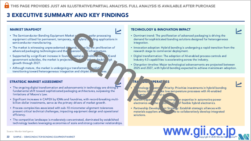
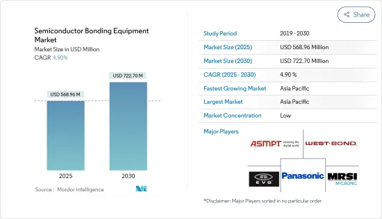
半導体ボンディング装置市場規模は、2025年に5億6,896万米ドルと推定され、予測期間中(2025~2030年)のCAGRは4.9%で、2030年には7億2,270万米ドルに達すると予測されています。
半導体ボンディング装置は、より高い効率、処理能力、より小さなフットプリントを持つ半導体チップへの需要の高まりによって用途が見いだされ、それによって予測期間中の市場需要を牽引しています。
主要ハイライト
- デジタル化の影響が拡大するにつれ、半導体市場は活況を呈しています。特筆すべきは、これがさらに5G展開を支援する政府プログラムをもたらしたことです。例えば、欧州委員会は5Gネットワークの重要性を早くから認識し、5G技術の開発と研究のために官民パートナーシップを設立しました。
- 今後10年間でチップ需要が急増することから、世界の半導体産業は2030年までに1兆米ドル産業になると予想されています。この成長は、企業や国が半導体製造、材料、研究に莫大な資金を注ぎ込み、ますますデータ中心になっていく広範な産業の成長を支えるチップとノウハウの安定供給を保証することによってもたらされています。
- 重要な技術部品を製造している半導体産業は、需要の急増で見出しを賑わしています。最近のウォール・ストリート・ジャーナル紙のレポートによると、半導体は原油、精製油、自動車に次いで世界第4位の貿易品(輸出入を合計したもの)にランクされています。これは、半導体が、エレクトロニクスや製造業、農業、医療、インフラ、エンターテインメント、輸送、通信、軍事システム、エネルギー管理、宇宙など、さまざまな産業におけるハイコンピューティング・用途に欠かせないからです。
- 製品が2つのダイやウエハーの接合を必要とする場合、いくつかの方法が用いられます。接合方法タイプそのものを選択するだけでなく、接合するものがウエハーかダイのどちらの形態であるかも決定しなければなりません。選択されたボンディングプロセスは、ボンディングの所有コストの主要因です。あるプロセスにとって最も重要な3つの要因は、ボンディングに必要な上流プロセスのコスト、ボンディングプロセスのサイクルタイム、ボンディングプロセスの歩留まりです。
- 世界のパンデミックの発生とCOVID-19の蔓延を抑えるための制限措置により、半導体ボンディング装置産業の世界のサプライチェーンは大きく混乱し、各社の生産能力に影響を与えました。COVID-19感染患者数はかなり減少したが、これらの部品の材料供給と需要に関する重大な問題に対処する必要があり、市場の成長に課題を残しています。
半導体ボンディング装置市場動向
パワーICとパワーディスクリート用途セグメントが大きな市場シェアを占める
- パワー半導体デバイスは、さまざまな用途で効率的な電力管理、変換、制御を促進します。省エネルギーと電力消費への関心の高まりが、パワー半導体デバイスの重要性を高めています。この市場を支えているのは、損失の低減、制御性の向上、耐久性の向上、標準状態や故障状態における信頼性の高い性能です。パワー半導体の需要が増加の一途をたどるなか、パワーICとボンディング技術の市場拡大も期待されています。
- このセグメントの成長を牽引しているのは、産業の急速なデジタル化と接続デバイスの増加です。これらのデバイスには、効率的な電源管理と高性能のパワー半導体デバイスが必要です。これらのデバイスを利用することで、最適な電力変換が達成され、エネルギー損失が削減され、電子システムの全体的なエネルギー効率が向上
- このセグメントは、高エネルギーで電力効率の高いデバイスに対する需要の高まりによって成長を遂げています。この需要は、ワイヤレスとポータブル電子製品の普及、自動車産業の電動化へのシフト、これらのデバイスの使用の増加によってさらに促進されています。
- 産業では、パワーモジュールや統合ソリューションへの傾斜が高まっています。パワー半導体のメーカーは、システム設計の合理化、部品点数の削減、システム全体の効率向上のために、スイッチ、ダイオード、ドライバなどのさまざまなパワーコンポーネントを統合した、コンパクトで高度に統合されたモジュールを開発しています。パワー半導体企業は、競合を維持するために、製品設計プロセスの早い段階で障害や市場動向を理解することで利益を得ることができます。ベンダーによるパワー半導体の生産増強投資の増加は、市場の拡大に影響を与えると予想されます。
- パワーICやディスクリートコンポーネントの大幅な開発により、電源管理の効率が向上しています。最近のシステムアーキテクチャの進歩により、AC-DC電源アダプタのサイズと部品点数が削減され、より効率的なAC-DC電源アダプタが開発されています。新しいPoE(Power-over-Ethernet)規格の導入は、より高い電力転送能力を可能にし、コネクテッド照明のような革新的なデバイス・カテゴリーの創出を促進しました。電子機器メーカーによる電力消費の最小化重視の高まりと、民生用電子機器からの需要の増加が、パワーICの必要性を高める主要因となっています。これらの要因は、ボンディング機器の需要を押し上げる可能性があります。
- スマートフォンのトランスミッション速度が大幅に上昇しており、処理要件に対応するためにバッテリーモジュールが必要となっています。電源アダプターにはディスクリート半導体が搭載されるようになり、バッテリー駆動デバイスの販売増加による需要急増が予想されます。IoT用途の成長は、ディスクリート半導体の需要をさらに促進すると予測されています。
- 例えば、Ericssonによると、世界のセルラーIoT接続は2022年に19億に達し、2027年には55億に達すると推定されています。5Gの進化に伴うスマートフォンの普及拡大が、市場の成長を牽引すると予想されます。
- 同様に、技術的に強化された連携デバイスを世界中の消費者に提供することを目的としたIoT用途の大幅な技術進歩も、市場の成長にプラスの影響を与えると予想されます。IoT用途の拡大により、スマートデバイスや小型半導体の普及が進み、その結果、先進的半導体ボンディング装置への需要が高まっている
- Ericssonは、主に短距離IoTデバイスの増加により、2022~2028年にかけて世界の接続デバイス数は約倍増すると述べています。このようなデバイスは、2028年までに約287億2,000万台になると予想されています。こうしたIoT接続デバイスの需要拡大に伴い、パワーICの需要も増加し、ボンディング装置市場の成長を高めると予想されます。
アジア太平洋が最も急成長する市場になる見込み
- 半導体産業はアジアの経済成長の重要な原動力として台頭してきました。その急速な拡大と技術進歩は、世界のサプライチェーンの重要なコンポーネントとなっています。
- アジア太平洋は、世界的に半導体鋳造の主要シェアを占めており、Samsung Electronics、TSMCなどの著名企業が進出しています。この地域では、韓国、台湾、日本、中国が大きなシェアを占めています。台湾は世界でも有数の鋳造シェアを占めており、半導体のバリューチェーンにおいて重要な地域です。同地域における半導体製造能力の拡大への投資の増加は、市場の成長を大きく助けると予想されます。
- 2023年9月、中国は半導体産業を後押しするために400億米ドルの基金を立ち上げました。中国は、世界のライバル、特に米国との差を縮めるため、国家が支援する投資ファンドの設立を計画しています。この構想は、一般にビッグ・ファンドとして知られる中国集積回路産業投資基金が管理する3つのファンドの中で最も重要なものとして発展する構えです。中国の習近平国家主席は、主に米国による輸出規制措置に対応して、半導体の自給自足を達成することの重要性を強調しました。今回のファンドは中国当局の承認を得ており、財務省は600億人民元(83億米ドル)を拠出します。
- 拡大する国内チップ需要に基づき、中国は米国を抜いて半導体産業における世界一の大国になると推定されています。半導体産業協会によると、2030年までに半導体市場の規模は倍増し、1兆米ドルを超えると予想されており、中国はその増加分の60%以上を占めるといいます。このような急激な成長は、半導体ボンディング装置に対する需要を増加させると予想されます。
- この新しい半導体工場は、ディスプレイドライバ、パワーマネージメントIC、マイクロコントローラ、高性能コンピューティング・ロジックなどの用途向けチップを製造し、コンピューティングやデータストレージ、自動車、ワイヤレス通信、人工知能などの市場で高まる需要に対応します。この工場は月産5万ウエハーの製造能力を持ち、2026年末までに最初のチップを出荷する予定です。
半導体ボンディング装置市場概要
半導体ボンディング装置市場は非常に細分化されており、EV Group、ASMPT Semiconductor Solutions、MRSI Systems(Myronic AB)、WestBond Inc.、Panasonic Holding Corporationなどの大手企業が参入しています。市場参入企業は、サステイナブル競争優位性を獲得し、製品ラインアップを強化するために、提携や買収に参加しています。
- 2023年11月-EVグループ(EVG)は、EVG本社拡大の次の段階の建設工事の完了を発表。マニュファクチャリングV」施設はEVGの機器部品製造部門として機能し、生産フロアと倉庫スペースを大幅に拡大します。マニュファクチャリングV施設の開設は、EVGの最新の拡大段階と投資を示すものです。EVGは、急成長する先進包装市場と3D/ヘテロジニアスインテグレーション市場をサポートするため、EVGのハイブリッドボンディングソリューションやその他のプロセスソリューション、プロセス開発サービスに対する継続的な高い需要の恩恵を受け続けています。
- 2023年9月-MRSI Systems(Mycronic AB)は、定評あるMRSI-7001プラットフォームの新バリエーション、MRSI 7001HFの発売を発表しました。7001HFは、接合時に最大500Nの力を加えることができる加熱式ボンドヘッドを特徴としています。この加熱式ボンドヘッドは、400℃の温度で上部から加熱することもできます。これにより、7001HFは、IC包装用パワー半導体焼結やIC包装用熱圧着ボンダなどの用途向けの高荷重ダイボンダーに最適なツールとなります。
その他の特典
- エクセル形式の市場予測(ME)シート
- 3ヶ月のアナリストサポート
目次
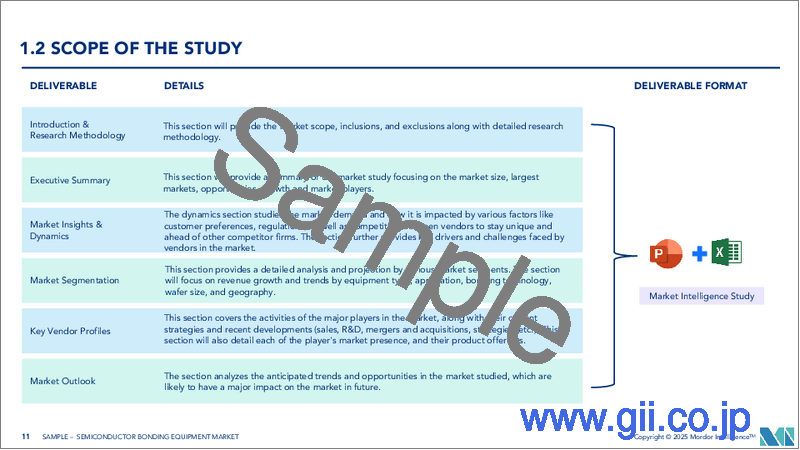
第1章 イントロダクション
- 調査の前提条件と市場定義
- 調査範囲
第2章 調査手法
第3章 エグゼクティブサマリー
第4章 市場洞察
- 市場概要
- 市場の魅力-ポーターのファイブフォース分析
- 供給企業の交渉力
- 買い手の交渉力
- 新規参入業者の脅威
- 代替品の脅威
- 競争企業間の敵対関係
- 産業バリューチェーン/サプライチェーン分析
- COVID-19の市場への影響
第5章 市場力学
- 市場の促進要因
- 半導体メーカーによる製造能力拡大のための投資の増加
- 様々な用途における半導体チップの需要増加
- 市場抑制要因
- 高い所有コスト
- 回路の小型化による複雑化
第6章 市場セグメンテーション
- タイプ別
- 永久ボンディング装置
- 一時ボンディング装置
- ハイブリッドボンディング装置
- 用途別
- 先進包装
- パワーICとパワーディスクリート
- フォトニックデバイス
- MEMSセンサとアクチュエータ
- エンジニア基板
- RFデバイス
- CMOSイメージセンサ(CIS)
- 地域別
- 北米
- 欧州
- アジア
- オーストラリア・ニュージーランド
- ラテンアメリカ
- 中東・アフリカ
第7章 競合情勢
- 企業プロファイル
- EV Group
- ASMPT Semiconductor Solutions
- MRSI Systems.(Myronic AB)
- WestBond Inc.
- Panasonic Holding Corporation
- Palomar Technologies
- Dr. Tresky AG
- BE Semiconductor Industries NV
- Fasford Technology Co.Ltd(Fuji Group)
- Kulicke and Soffa Industries Inc.
- DIAS Automation(HK)Ltd
- Shibaura Mechatronics Corporation
- SUSS MicroTec SE
- Tokyo Electron Limited
第8章 投資分析
第9章 市場の将来
The Semiconductor Bonding Equipment Market size is estimated at USD 568.96 million in 2025, and is expected to reach USD 722.70 million by 2030, at a CAGR of 4.9% during the forecast period (2025-2030).
Semiconductor bonding equipment finds application owing to the rising demand for semiconductor chips with higher efficiency, processing power, and smaller footprint, thereby driving the demand for the market during the forecast period.
Key Highlights
- As the impact of digitalization has increased, semiconductor markets have boomed. Notably, this has further resulted in government programs to support the 5G deployment. For instance, the European Commission recognized the importance of the 5G network early and established a public-private partnership to develop and research 5G technology.
- With chip demand set to surge over the coming decade, the global semiconductor industry is expected to become a trillion-dollar industry by 2030. This growth is favored by companies and countries funneling vast sums of money into semiconductor manufacturing, materials, and research to guarantee a constant supply of chips and know-how to support growth across a broad swath of increasingly data-centric industries.
- The semiconductor industry, which makes crucial technological components, has been hitting the headlines due to a rampant demand increase. A recent Wall Street Journal report shows that semiconductors rank as the world's fourth-largest traded product (imports and exports, counted), after crude oil, refined oil, and cars. This is because semiconductors are critical for high-computing applications in various industries, including electronics and manufacturing industries, agriculture, healthcare, infrastructure, entertainment, transportation, telecommunications, military systems, energy management, and space, to name just a few.
- Several methods might be used when a product needs the bonding of two dies or wafers. Not only does the type of bonding method itself have to be selected, but it must also be decided whether the items being bonded will be in wafer or die form. The selected bonding process is the primary driver for the cost of ownership of bonding. For a given process, the three most important factors are the cost of the upstream process needed for bonding, the cycle time of the bonding process, and the yield of the bonding process.
- With the global outbreak of the pandemic and restrictive measures taken to control the spread of COVID-19, the global supply chain of the semiconductor bonding equipment industry was significantly disrupted, impacting the production capabilities of various companies. Although the number of COVID-19-infected patients decreased considerably, salient issues with materials supply and demand for these components still need to be addressed, challenging the market's growth.
Semiconductor Bonding Equipment Market Trends
Power IC and Power Discrete Application Segment Holds Significant Market Share
- Power semiconductor devices facilitate efficient power management, conversion, and control across various applications. The increasing focus on energy conservation and power consumption is increasing the significance of power semiconductor devices. The market is supported by reduced losses, enhanced controllability, greater durability, and reliable performance in standard and fault conditions. As the demand for power semiconductors continues to rise, there is also an expected increase in the market for power ICs and bonding technology.
- The segment's growth is driven by the rapid digitization of industries and the increasing number of connected devices. These devices necessitate efficient power management and high-performance power semiconductor devices. By utilizing these devices, optimal power conversion is achieved, energy losses are reduced, and the overall energy efficiency of electronic systems is enhanced.
- The segment is experiencing growth due to the rising demand for high-energy and power-efficient devices. This demand is further fueled by the prevalence of wireless and portable electronic products, the automotive industry's shift toward electrification, and the increased use of these devices.
- The industry has a rising inclination toward power modules and integrated solutions. Manufacturers of power semiconductors are creating compact, highly integrated modules that merge various power components like switches, diodes, and drivers to streamline system design, lower component quantity, and improve overall system efficiency. Power semiconductor firms stand to gain by understanding the obstacles and market trends early in the product design process to remain competitive. The increasing investments by vendors to boost power semiconductor production are anticipated to affect the market's expansion.
- A significant development in power IC and discrete components enhances power management efficiency. Recent advancements in system architectures have led to more efficient AC-DC power adapters with reduced size and component numbers. Introducing new Power-over-Ethernet (PoE) standards has enabled higher power transfer capabilities, facilitating the creation of innovative device categories like connected lighting. The growing emphasis on minimizing electricity consumption by electronics manufacturers and the increasing demand from consumer electronics are the primary drivers behind the necessity for Power ICs. These factors could potentially boost the demand for bonding equipment.
- There is a significant rise in smartphone transmission speeds, necessitating battery modules to accommodate the processing requirements. Power adapters are now incorporating discrete semiconductors, leading to an anticipated surge in demand driven by the increasing sales of battery-powered devices. The growth of IoT applications is projected to propel the demand for discrete semiconductors further.
- For example, according to Ericsson, global cellular IoT connections reached 1.9 billion in 2022 and are estimated to reach 5.5 billion by 2027. The increasing penetration of smartphones with the evolution of 5G is expected to drive the market's growth.
- Similarly, the market's growth is expected to be positively influenced by the significant technological advancements in IoT applications, which aim to provide technologically enhanced linked devices to consumers worldwide. The expansion of IoT applications has increased the prevalence of smart devices and small semiconductors, consequently driving the demand for advanced semiconductor bonding equipment.
- Ericsson stated that the number of connected devices globally will nearly double from 2022 to 2028, primarily due to the rise in short-range IoT devices. It is expected that there will be approximately 28.72 billion such devices by 2028. With the growing demand for these IoT-connected devices, the demand for power ICs is expected to rise, thereby enhancing the growth of the bonding equipment market.
Asia-Pacific is Expected to be the Fastest Growing Market
- The semiconductor industry has emerged as a critical driver of economic growth in Asia. Its rapid expansion and technological advancements have become an important component of the global supply chain.
- Asia-Pacific holds a major share of semiconductor foundries globally, with the region having the presence of prominent companies like Samsung Electronics, TSMC, etc. South Korea, Taiwan, Japan, and China have significant market shares in the region. Taiwan holds a prominent share of the foundries in the world and is a vital region in the semiconductor value chain. The increasing investments in the expansion of semiconductor manufacturing capacities in the region are expected to aid the market's growth significantly.
- In September 2023, China launched a USD 40 billion fund to boost the semiconductor industry. China plans to establish a state-backed investment fund to narrow the gap with global rivals, especially the United States. This initiative is poised to evolve as the most significant of the trio of funds managed by the China Integrated Circuit Industry Investment Fund, generally known as the Big Fund. President Xi Jinping of China stressed the critical importance of achieving semiconductor self-sufficiency, primarily in response to export control measures imposed by the United States. The latest fund obtained approval from Chinese authorities, with the finance ministry committing CNY 60 billion (USD 8.30 billion).
- Based on its expanding domestic chip demand, China is estimated to overtake the United States as the world's top powerhouse in the semiconductor industry. By 2030, the semiconductor market is expected to double in size to reach more than USD 1 trillion, with China contributing over 60% of that increase, according to the Semiconductor Industry Association. Such exponential growth is anticipated to increase demand for semiconductor bonding equipment.
- The new semiconductor fab would fabricate chips for applications like display drivers, power management IC, microcontrollers, and high-performance computing logic, addressing the growing demand in markets like computing and data storage, automotive, wireless communication, and artificial intelligence. This fab claims to have a manufacturing capacity of up to 50,000 wafers per month, and the first chip will come out of the facility before the end of 2026.
Semiconductor Bonding Equipment Market Overview
The semiconductor bonding equipment market is highly fragmented, with major players like EV Group, ASMPT Semiconductor Solutions, MRSI Systems (Myronic AB), WestBond Inc., and Panasonic Holding Corporation. Market players participate in partnerships and acquisitions to gain sustainable competitive advantage and enhance their product offerings.
- November 2023 - The EV Group (EVG) announced the completion of construction works for the next phase of the expansion of EVG corporate headquarters. The "Manufacturing V" facility serves as EVG's manufacturing department for equipment components and offers a significant expansion of production floor and warehouse space. The opening of the Manufacturing V facility marks the latest expansion phase and investment of EVG, which continues to benefit from the continuing high demand for EVG's hybrid bonding solutions and other process solutions, as well as process development services, to support the fast-growing advanced packaging market and 3D / heterogeneous integration market.
- September 2023 - MRSI Systems (Mycronic AB) announced the launch of the new variant of the well-established MRSI-7001 platform, the MRSI 7001HF. The 7001HF features a heated bond head capable of applying up to 500N forces during bonding. The heated bond head also provides heating from the top at a temperature of 400°C. This makes the 7001HF the perfect tool for high-force die bonders for applications such as power semiconductor sintering for IC packaging or thermocompression bonders for IC packaging.
Additional Benefits:
- The market estimate (ME) sheet in Excel format
- 3 months of analyst support
TABLE OF CONTENTS
1 INTRODUCTION
- 1.1 Study Assumptions and Market Definition
- 1.2 Scope of the Study
2 RESEARCH METHODOLOGY
3 EXECUTIVE SUMMARY
4 MARKET INSIGHTS
- 4.1 Market Overview
- 4.2 Market Attractiveness - Porter's Five Forces Analysis
- 4.2.1 Bargaining Power of Suppliers
- 4.2.2 Bargaining Power of Buyers
- 4.2.3 Threat of New Entrants
- 4.2.4 Threat of Substitutes
- 4.2.5 Intensity of Competitive Rivalry
- 4.3 Industry Value Chain/Supply Chain Analysis
- 4.4 Impact of COVID-19 on the Market
5 Market Dynamics
- 5.1 Market Driver
- 5.1.1 Increasing Investment by Semiconductor Manufacturers to Expand their Manufacturing Capacity
- 5.1.2 Rising Demand for Semiconductor Chips across Various Application
- 5.2 Market Restraints
- 5.2.1 High Cost of Ownership
- 5.2.2 Increased Complexity Owing to Miniaturization of Circuits
6 MARKET SEGMENTATION
- 6.1 By Type
- 6.1.1 Permanent Bonding Equipment
- 6.1.2 Temporary Bonding Equipment
- 6.1.3 Hybrid Bonding Equipment
- 6.2 By Application
- 6.2.1 Advanced Packaging
- 6.2.2 Power IC and Power Discrete
- 6.2.3 Photonic Devices
- 6.2.4 MEMS Sensors and Actuators
- 6.2.5 Engineered Substrates
- 6.2.6 RF Devices
- 6.2.7 CMOS Image Sensors (CIS)
- 6.3 By Geography
- 6.3.1 North America
- 6.3.2 Europe
- 6.3.3 Asia
- 6.3.4 Australia and New Zealand
- 6.3.5 Latin America
- 6.3.6 Middle East and Africa
7 COMPETITIVE LANDSCAPE
- 7.1 Company Profiles
- 7.1.1 EV Group
- 7.1.2 ASMPT Semiconductor Solutions
- 7.1.3 MRSI Systems. (Myronic AB)
- 7.1.4 WestBond Inc.
- 7.1.5 Panasonic Holding Corporation
- 7.1.6 Palomar Technologies
- 7.1.7 Dr. Tresky AG
- 7.1.8 BE Semiconductor Industries NV
- 7.1.9 Fasford Technology Co.Ltd (Fuji Group)
- 7.1.10 Kulicke and Soffa Industries Inc.
- 7.1.11 DIAS Automation (HK) Ltd
- 7.1.12 Shibaura Mechatronics Corporation
- 7.1.13 SUSS MicroTec SE
- 7.1.14 Tokyo Electron Limited
