
|
市場調査レポート
商品コード
1479763
サブ100nmリソグラフィ:世界市場の分析と戦略的課題Sub-100nm Lithography: Market Analysis and Strategic Issues |
||||||
|
|||||||
| サブ100nmリソグラフィ:世界市場の分析と戦略的課題 |
|
出版日: 2026年01月01日
発行: Information Network
ページ情報: 英文
納期: 2~3営業日
|

全表示
- 概要
- 図表
- 目次
促進要因
半導体技術のノードが縮小し、より小型で複雑な半導体デバイスへの需要が増加するにつれて、複数の促進要因がこれらの課題に対応するリソグラフィ技術の進歩を後押ししています。
技術の微細化:新しい技術ノードが登場するたびに、半導体メーカーは性能、電力効率、密度を向上させるため、トランジスタと配線のサイズを縮小することを目指しています。このような微細化を高精度と高解像度で実現するためには、先進のリソグラフィ技術が不可欠であり、次世代リソグラフィツールの開発が推進されています。
EUVリソグラフィの採用:EUVリソグラフィは、従来の光リソグラフィよりも波長が短いため、より微細で複雑なパターンを形成できます。ノードの微細化に伴い、必要なパターニング解像度を達成するためには、EUVリソグラフィの採用がますます必要となっています。
マルチパターニング技術:フィーチャーサイズが光リソグラフィの限界に近づくにつれて、SADP、SAQP、MBMLなどのマルチパターニング技術が、所望のフィーチャ密度とピッチを達成するために不可欠となります。これらの技術では、複雑なパターンを形成するために複数の露光工程とエッチング工程が必要となるため、先進のリソグラフィソリューションの必要性が高まっています。
解像度向上技術(RET):パターン転写の解像度と忠実度を向上させるため、リソグラフィツールには、光近接効果補正(OPC)、位相シフトマスク(PSM)、ソースマスク最適化(SMO)などの解像度向上技術が組み込まれています。これらのRETは、回折やその他の光学的制限の影響を緩和するのに役立ち、先進のノードにおけるより微細なフィーチャーの製造を可能にします。
プロセス制御と歩留まりの改善:フィーチャーサイズが小さくなるにつれ、厳密なプロセス制御を維持することがますます課題となっています。先進のリソグラフィツールには、均一性、オーバーレイ精度、欠陥の低減を保証するための先進の計測およびプロセス制御機能が組み込まれています。これらの機能は、先進のノードで高い歩留まりと製造一貫性を達成するために不可欠です。
新興用途と市場需要:AI、5G接続性、自動運転車、IoTデバイスなどの新技術は、特定の性能要件を備えた特殊な半導体デバイスの需要を促進しています。先進のリソグラフィソリューションは、これらの用途に必要な複雑な構造や材料をパターニングするために不可欠であり、リソグラフィ技術の革新を促進しています。
当レポートの必要性
半導体リソグラフィは半導体製造の礎石であり、現代の電子を支える複雑な半導体デバイスの製造において極めて重要なプロセスです。半導体技術の進歩とともにリソグラフィ技術も進化し、解像度、精度、スループットの限界に課題することで、これまで以上に微細で複雑な半導体構造の製造を可能にしています。
半導体産業は、より高性能でエネルギー効率の高い電子デバイスの需要により、微細化のあくなき追求を示しています。極端紫外線(EUV)リソグラフィ、マルチパターニング、液浸リソグラフィなどの先進のリソグラフィ技術は、10ナノメートル以下の微細化を実現する上で極めて重要な役割を果たし、半導体製造能力の限界を押し広げています。
当レポートでは、世界の半導体リソグラフィ市場を包括的に分析し、市場規模、成長促進要因、競合情勢、新たな市場機会に関する考察を提供しています。
目次
第1章 イントロダクション
第2章 エグゼクティブサマリー
- 主要課題のサマリー
- 市場機会のサマリー
第3章 リソグラフィの課題と動向
- 光学システム
- イントロダクション
- ステップアンドリピートアライナー
- 深紫外線(DUV)
- EUV
- ナノインプリントリソグラフィ
- X線リソグラフィ
- 電子ビームリソグラフィ
- イオンビームリソグラフィ
第4章 ユーザーとサプライヤーの戦略
- リソグラフィのニーズの決定
- ベンダーのベンチマーク
- 価格
- ベンダーのコミットメントと姿勢
- ベンダーの能力
- システムの能力
- 機器評価中のベンダーからのフィードバック
- 機器生産中のベンダーからのフィードバック
- 競合環境
- クラス1クリーンルーム向け機器
- 未来の工場向け機器
- 機会
第5章 市場予測
- 促進要因
- 技術動向
- 経済動向
- 光学的限界
- 市場予測の前提条件
- 市場予測
List of Tables
- 3.1. Wavelength "Generations"
- 3.2. Characteristics of X-Ray Systems
- 5.1. Worldwide Capital Spending
- 5.2. DRAM Lithographic Requirements
- 5.3. Worldwide Optical Stepper Market
- 5.4. Worldwide Stepper Market Shares
List of Figures
- 1.1. Lithographic Equipment Requirements for DRAMs
- 3.1. Lithography Options For MPUs/DRAMs
- 3.2. Lithography Options For Flash
- 3.3. Illustration of Stepper Exposure System
- 3.4. Lens Arrangement For Submicron Features
- 3.5. Excimer Laser Evolution
- 3.6. EUV Lithography
- 3.7. Thermoplastic Nanoimprint Lithography Process
- 3.8. Step And Flash Nanoimprint Lithography Process
- 3.9. Illustration of X-Ray Lithography
- 3.10. Schematic Of Scalpel Electron Beam System
- 3.11. Multi-Source E-Beam Lithography
- 3.12. Ion Projection Lithography System
- 4.1. Manufacturing Costs Per Exposure Station
- 5.1. Lithography Market Vs Equipment Market
- 5.2. Lithography Double Exposure Technique
- 5.3. Lithography Requirements
- 5.4. Lithography Extensions
- 5.5. Lithography Cost of Ownership
- 5.6. Segmentation of Stepper/Scan Shipments
- 5.7. Market Shares of Vendors (Units)
- 5.8. Unit Market Shares of Vendors
- 5.9. Worldwide I-Line Market Shares
- 5.10. Worldwide 248nm Market Shares
- 5.11. Worldwide 193nm Dry Market Shares
- 5.12. Worldwide 193nm Wet Market Shares
- 5.13. Market Shares of Vendors (Revenues)
Driving Forces
As semiconductor technology nodes shrink and demand for smaller and more complex semiconductor devices increases, several driving forces push the advancement of lithography technology to meet these challenges:
Technological Scaling: With each new technology node, semiconductor manufacturers aim to reduce the size of transistors and interconnects to improve performance, power efficiency, and density. Advanced lithography techniques are essential for patterning these smaller features with high precision and resolution, driving the development of next-generation lithography tools.
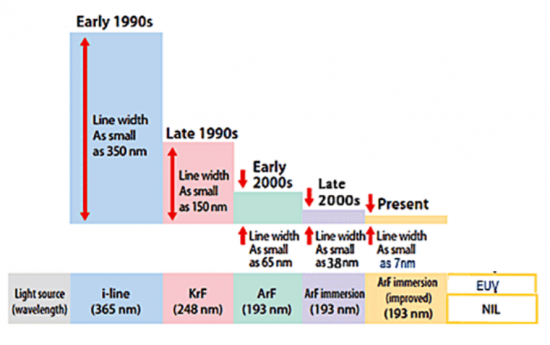
EUV Lithography Adoption: Extreme ultraviolet (EUV) lithography has emerged as a leading candidate for patterning critical layers in advanced semiconductor manufacturing processes. EUV offers shorter wavelengths than traditional optical lithography, enabling the fabrication of smaller feature sizes and more complex patterns. As nodes get smaller, the adoption of EUV lithography becomes increasingly necessary to achieve the required patterning resolution.
Multi-Patterning Techniques: As feature sizes approach the limits of optical lithography, multipatterning techniques such as self-aligned double patterning (SADP), self-aligned quadruple patterning (SAQP), and multi-beam maskless lithography (MBML) become indispensable for achieving the desired feature density and pitch. These techniques involve multiple exposure and etching steps to create intricate patterns, driving the need for advanced lithography solutions.
Resolution Enhancement Technologies (RET): To improve the resolution and fidelity of pattern transfer, lithography tools incorporate resolution enhancement techniques such as optical proximity correction (OPC), phase-shift masks (PSM), and source mask optimization (SMO). These RETs help mitigate the effects of diffraction and other optical limitations, enabling the fabrication of finer features at advanced nodes.
Process Control and Yield Improvement: As feature sizes shrink, maintaining tight process control becomes increasingly challenging. Advanced lithography tools incorporate sophisticated metrology and process control capabilities to ensure uniformity, overlay accuracy, and defect reduction. These capabilities are essential for achieving high yields and manufacturing consistency at advanced nodes.
Emerging Applications and Market Demand: Emerging technologies such as artificial intelligence (AI), 5G connectivity, autonomous vehicles, and IoT devices drive the demand for specialized semiconductor devices with specific performance requirements. Advanced lithography solutions are essential for patterning the complex structures and materials required for these applications, driving innovation in lithography technology.
The Need for This Report
Semiconductor lithography stands as a cornerstone in the realm of semiconductor manufacturing, serving as a pivotal process in the creation of intricate semiconductor devices that power modern electronics. As semiconductor technology advances, lithography techniques evolve in tandem, pushing the boundaries of resolution, precision, and throughput to enable the fabrication of ever-smaller and more complex semiconductor structures. This comprehensive report delves into the multifaceted landscape of semiconductor lithography, exploring key technologies, market trends, industry challenges, and future prospects shaping the semiconductor lithography ecosystem.
The semiconductor industry is witnessing a relentless pursuit of miniaturization, driven by the demand for higher-performance and more energy-efficient electronic devices. As feature sizes shrink to nanoscale dimensions, lithography emerges as a critical enabler, allowing semiconductor manufacturers to pattern intricate circuit designs with unparalleled precision. Advanced lithography techniques such as extreme ultraviolet (EUV) lithography, multiple patterning, and immersion lithography play pivotal roles in achieving sub-10 nanometer feature sizes, pushing the limits of semiconductor manufacturing capabilities.
In addition to technological advancements, the semiconductor lithography market is influenced by a myriad of factors, including market dynamics, regulatory policies, and industry collaborations. This report provides a comprehensive analysis of the global semiconductor lithography market, offering insights into market size, growth drivers, competitive landscape, and emerging opportunities. Through a detailed examination of lithography equipment, materials, and processes, stakeholders gain a deeper understanding of the evolving semiconductor lithography landscape and its impact on the semiconductor industry.
Furthermore, the report explores key challenges and bottlenecks facing semiconductor lithography, ranging from mask complexity and defect reduction to cost constraints and yield optimization. By identifying critical issues and potential solutions, stakeholders can devise strategies to mitigate risks and capitalize on growth opportunities in the semiconductor lithography market.
As semiconductor lithography continues to evolve in response to technological advancements and market demands, stakeholders across the semiconductor ecosystem must stay abreast of the latest developments and trends shaping the industry. This report serves as a valuable resource for semiconductor manufacturers, equipment suppliers, investors, and other industry participants seeking actionable insights into the dynamic landscape of semiconductor lithography. Through comprehensive analysis and strategic recommendations, this report empowers stakeholders to navigate the complex terrain of semiconductor lithography and drive innovation in semiconductor manufacturing.
Report Coverage
This report provides a detailed analysis of the global semiconductor lithography market, including historical data, current market size, and projected growth trends. It may also include market segmentation based on technology, end-user industry, and geographical regions.
It explores the various lithography technologies utilized in semiconductor manufacturing, such as optical lithography, extreme ultraviolet (EUV) lithography, multiple patterning, nanoimprint lithography, and others. This section delves into the principles, advancements, and applications of each technology.
Market Segmentation: Unit and Revenue segments the semiconductor lithography market based on technology types are forecast by:
|
|
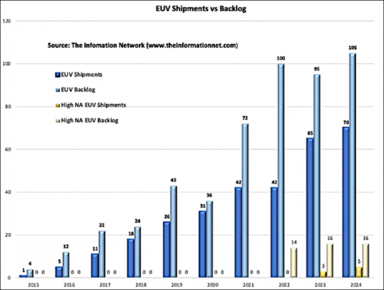
The report provides insights into market share of lithography vendors by equipment type including revenue and unit shipments. Market shares by vendor are provided since 1992. The report identifies and analyzes current and emerging trends driving the semiconductor lithography market, such as node migration, China sanctions, and new semiconductor materials, particularly silicon carbide.
Table of Contents
Chapter 1. Introduction
- 1.1. The Need For This Report
Chapter 2. Executive Summary
- 2.1. Summary of Major Issues
- 2.2. Summary of Market Opportunities
Chapter 3. Lithography Issues And Trends
- 3.1. Optical Systems
- 3.1.1. Introduction
- 3.1.2. Step-and-Repeat Aligners
- 3.1.3. Deep Ultraviolet (DUV)
- 3.2. EUV
- 3.5. Nano-Imprint Lithography
- 3.4. X-Ray Lithography
- 3.3. Electron Beam Lithography
- 3.4. Ion Beam Lithography
Chapter 4. User - Supplier Strategies
- 4.1. Determining Lithography Needs
- 4.2. Benchmarking a Vendor
- 4.2.1. Pricing
- 4.2.2. Vendor Commitment and Attitudes
- 4.2.3. Vendor Capabilities
- 4.2.4. System Capabilities
- 4.2.5. Vendor Feedback During Equipment Evaluation
- 4.2.6. Vendor Feedback During Device Production
- 4.3. Competitive Environment
- 4.4. Equipment For Class 1 Cleanrooms
- 4.5. Equipment For the Factory of the Future
- 4.6. Opportunities
Chapter 5. Market Forecast
- 5.1. Driving Forces
- 5.1.1. Technical Trends
- 5.1.2. Economic Trends
- 5.1.3. Optical Limitations
- 5.2. Market Forecast Assumptions
- 5.3. Market Forecast

