
リソグラフィ装置市場の機会、成長促進要因、産業動向分析、2025年~2034年の予測
Lithography Equipment Market Opportunity, Growth Drivers, Industry Trend Analysis, and Forecast 2025-2034- 発行日
- ページ情報
- 英文 210 Pages
- 納期
- 2~3営業日
- 商品コード
- 1699355
- カスタマイズ可能 お客様のご希望に応じて、既存データの加工や未掲載情報(例:国別セグメント)の追加などの対応が可能です。詳細はお問い合わせください。
- 翻訳ツール提供対象 PDF対応AI翻訳ツールの無料貸し出しサービスのご利用が可能です
概要
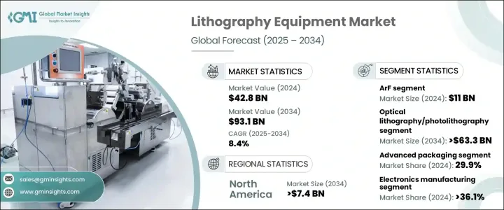
リソグラフィ装置の世界市場規模は2024年に428億米ドルとなり、2025年から2034年にかけてCAGR 8.4%で成長すると予測されています。
この成長は、特にコンシューマーエレクトロニクスにおいて、先進的でコンパクトな半導体部品への需要が急増していることが背景にあります。現代の電子機器は進化を続けており、メーカーは処理能力、エネルギー効率、総合性能を高めるために半導体設計の限界に課題しています。この複雑化により、最先端のリソグラフィ技術の採用が推進され、優れた機能を持つ高密度チップの生産が保証されています。
半導体業界ではチップ製造プロセスが急速に進歩しており、リソグラフィ装置は次世代デバイスの実現に重要な役割を果たしています。人工知能、モノのインターネット(IoT)、5G技術の統合が進むにつれ、高性能チップへのニーズがさらに高まり、高度なリソグラフィ・ソリューションへの強い需要が生まれています。さらに、半導体業界の競争は、リソグラフィ技術の絶え間ない革新をもたらし、半導体製造においてより高い精度と効率を達成することを可能にしています。半導体産業がより複雑なアーキテクチャに移行するにつれ、リソグラフィ装置への依存は拡大し続け、技術進歩の重要な原動力となっています。
| 市場範囲 | |
|---|---|
| 開始年 | 2024 |
| 予測年 | 2025-2034 |
| 開始金額 | 428億米ドル |
| 予測金額 | 931億米ドル |
| CAGR | 8.4% |
市場は技術別にArF、KrF、i線、ArF液浸、極端紫外線(EUV)リソグラフィに区分されます。このうちArF分野は、2024年の市場規模が110億米ドルに達し、特にビデオストリーミング、オンラインゲーム、仮想現実や拡張現実などの急成長産業での応用により、大きな成長が見込まれています。ArF技術は、深紫外(DUV)リソグラフィの性能を向上させ、高性能・高密度の半導体デバイスの製造に不可欠です。強力で効率的なチップへのニーズが高まるにつれ、ArFセグメントはさらに拡大し、半導体イノベーションを促進する役割を強化すると予想されます。
リソグラフィ装置はさらに、光リソグラフィ、電子ビームリソグラフィ、マスクアライナー、イオンリソグラフィ、X線リソグラフィ、ナノインプリントリソグラフィなど、タイプ別に分類されます。このうち、フォトリソグラフィとしても知られる光リソグラフィは依然として支配的なセグメントであり、2034年までに633億米ドルに達すると予測されています。広く採用されている理由は、既存の半導体製造設備にシームレスに統合できるため、チップメーカーにとって費用対効果が高く拡張性の高いソリューションとなっているためです。継続的な進歩により解像度と効率が向上しているため、光リソグラフィは半導体製造に好まれる選択肢であり続け、今後数年間も市場での強い存在感が確保されます。
北米のリソグラフィ装置市場は大幅に成長し、2034年には74億米ドルに達すると予測されています。この急成長は、自動車、家電、データセンターなどの産業における半導体需要の高まりが原動力となっています。サプライチェーンの強靭性を強化し、半導体製造を国内地域に呼び戻す取り組みが、市場拡大にさらに拍車をかけています。さらに、研究開発に重点を置く北米は、高度に熟練した労働力と相まってリソグラフィ技術の革新を加速させており、この地域を半導体進歩の重要な拠点として位置付けています。
目次
第1章 調査手法と調査範囲
第2章 エグゼクティブサマリー
第3章 業界洞察
- エコシステム分析
- 業界への影響要因
- 促進要因
- コンシューマーエレクトロニクスにおける高度化・小型化された半導体部品への需要の高まり
- リソグラフィ・プロセスの技術進歩
- 自動車の電動化需要の増加と電気自動車の世界的普及
- 世界のIoTとAI技術への動向の高まり
- 小型で電力効率の高いデバイスへの需要の高まり
- 業界の潜在的リスク&課題
- 製造コストの高さ
- セキュリティ上の懸念
- 促進要因
- 成長可能性分析
- 規制状況
- 技術情勢
- 今後の市場動向
- ギャップ分析
- ポーター分析
- PESTEL分析
第4章 競合情勢
- イントロダクション
- 企業シェア分析
- 主要市場プレーヤーの競合分析
- 競合のポジショニングマトリックス
- 戦略ダッシュボード
第5章 市場推計・予測:技術別、2021年~2034年
- 主要動向
- ArF
- KrF
- i線
- ArF液浸
- 極端紫外線(EUV)リソグラフィ
第6章 市場推計・予測:装置別、2021年~2034年
- 主要動向
- 光リソグラフィ/フォトリソグラフィ
- マスクアライナー
- 電子ビームリソグラフィ
- イオンリソグラフィ
- X線リソグラフィ
- ナノインプリントリソグラフィ
第7章 市場推計・予測:用途別、2021年~2034年
- 主要動向
- 先進パッケージング
- MEMSデバイス
- LEDデバイス
- その他
第8章 市場推計・予測:最終用途別、2021年~2034年
- 主要動向
- エレクトロニクス製造
- ヘルスケア・ライフサイエンス
- 自動車産業
- 通信業界
- その他
第9章 市場推計・予測:地域別、2021年~2034年
- 主要動向
- 北米
- 米国
- カナダ
- 欧州
- 英国
- ドイツ
- フランス
- イタリア
- スペイン
- アジア太平洋
- 中国
- 日本
- インド
- 韓国
- ニュージーランド
- 台湾
- ラテンアメリカ
- ブラジル
- メキシコ
- 中東・アフリカ
- サウジアラビア
- アラブ首長国連邦
- イスラエル
- 南アフリカ
第10章 企業プロファイル
- ASML Holding N.V.
- Nikon Corporation
- Canon Inc.
- Veeco Instruments Inc.
- SUSS MicroTec AG
- EV Group
- SCREEN Holdings Co., Ltd.
- Onto Innovation Inc.
- JEOL Ltd
- Neutronix Quintel Inc.(NXQ)
- Advantest
- Shanghai Micro Electronics Equipment(Group)Co., Ltd.
目次
The Global Lithography Equipment Market was valued at USD 42.8 billion in 2024 and is projected to grow at a CAGR of 8.4% from 2025 to 2034. This growth is fueled by the surging demand for advanced and compact semiconductor components, particularly in consumer electronics. As modern electronic devices continue to evolve, manufacturers are pushing the boundaries of semiconductor design to enhance processing power, energy efficiency, and overall performance. This growing complexity is driving the adoption of cutting-edge lithography technologies, ensuring the production of high-density chips with superior functionality.
The semiconductor industry is experiencing rapid advancements in chip manufacturing processes, with lithography equipment playing a crucial role in enabling next-generation devices. The increasing integration of artificial intelligence, the Internet of Things (IoT), and 5G technology is further amplifying the need for high-performance chips, creating a strong demand for advanced lithography solutions. Moreover, the competitive nature of the semiconductor industry has led to continuous innovation in lithography techniques, allowing manufacturers to achieve higher precision and efficiency in semiconductor fabrication. As the semiconductor industry moves toward more intricate architectures, the reliance on lithography equipment continues to expand, making it a key driver of technological progress.
| Market Scope | |
|---|---|
| Start Year | 2024 |
| Forecast Year | 2025-2034 |
| Start Value | $42.8 Billion |
| Forecast Value | $93.1 Billion |
| CAGR | 8.4% |
The market is segmented by technology into ArF, KrF, i-line, ArF immersion, and Extreme Ultraviolet (EUV) Lithography. Among these, the ArF segment was valued at USD 11 billion in 2024 and is set for significant growth, particularly due to its applications in fast-growing industries like video streaming, online gaming, and virtual and augmented reality. ArF technology delivers enhanced performance within Deep Ultraviolet (DUV) lithography, which is essential for producing high-performance, high-density semiconductor devices. As the need for powerful and efficient chips increases, the ArF segment is expected to expand further, reinforcing its role in driving semiconductor innovation.
Lithography equipment is further categorized by type, including optical lithography, electron beam lithography, mask aligners, ion lithography, X-ray lithography, and nanoimprint lithography. Among these, optical lithography, also known as photolithography, remains the dominant segment and is projected to reach USD 63.3 billion by 2034. Its widespread adoption is attributed to its seamless integration into existing semiconductor production facilities, making it a cost-effective and scalable solution for chipmakers. With continuous advancements improving resolution and efficiency, optical lithography remains a preferred choice for semiconductor manufacturing, ensuring its strong market presence in the years ahead.
North America lithography equipment market is set for substantial growth, projected to reach USD 7.4 billion by 2034. This surge is driven by rising semiconductor demand across industries such as automotive, consumer electronics, and data centers. Efforts to strengthen supply chain resilience and bring semiconductor manufacturing back to domestic regions are further fueling market expansion. Additionally, North America's emphasis on research and development, coupled with a highly skilled workforce, is accelerating innovation in lithography technology, positioning the region as a key hub for semiconductor advancements.
Table of Contents
Chapter 1 Methodology and Scope
- 1.1 Market scope and definitions
- 1.2 Research design
- 1.2.1 Research approach
- 1.2.2 Data collection methods
- 1.3 Base estimates and calculations
- 1.3.1 Base year calculation
- 1.3.2 Key trends for market estimation
- 1.4 Forecast model
- 1.5 Primary research and validation
- 1.5.1 Primary sources
- 1.5.2 Data mining sources
Chapter 2 Executive Summary
- 2.1 Industry 360° synopsis
Chapter 3 Industry Insights
- 3.1 Industry ecosystem analysis
- 3.2 Industry impact forces
- 3.2.1 Growth drivers
- 3.2.1.1 Rising demand for advanced and miniaturized semiconductor components in consumer electronics
- 3.2.1.2 Technological advancements in the lithography process
- 3.2.1.3 Increasing demand for electrification in vehicles and the global proliferation of electric vehicles
- 3.2.1.4 Increasing trend toward IoT and AI technology around the globe
- 3.2.1.5 Growing demand for Compact and Power-Efficient Devices
- 3.2.2 Industry pitfalls and challenges
- 3.2.2.1 High production cost
- 3.2.2.2 Security concerns
- 3.2.1 Growth drivers
- 3.3 Growth potential analysis
- 3.4 Regulatory landscape
- 3.5 Technology landscape
- 3.6 Future market trends
- 3.7 Gap analysis
- 3.8 Porter's analysis
- 3.9 PESTEL analysis
Chapter 4 Competitive Landscape, 2024
- 4.1 Introduction
- 4.2 Company market share analysis
- 4.3 Competitive analysis of major market players
- 4.4 Competitive positioning matrix
- 4.5 Strategy dashboard
Chapter 5 Market Estimates and Forecast, By Technology, 2021 – 2034 (USD Mn)
- 5.1 Key trends
- 5.2 ArF
- 5.3 KrF
- 5.4 i-line
- 5.5 Arf immersion
- 5.6 Extreme Ultraviolet (EUV) Lithography
Chapter 6 Market Estimates and Forecast, By Equipment, 2021 – 2034 (USD Mn)
- 6.1 Key trends
- 6.2 Optical Lithography/Photolithography
- 6.3 Mask aligners
- 6.4 Electron beam lithography
- 6.5 Ion lithography
- 6.6 X-Ray lithography
- 6.7 Nanoimprint lithography
Chapter 7 Market Estimates and Forecast, By Application, 2021 – 2034 (USD Mn)
- 7.1 Key trends
- 7.2 Advanced packaging
- 7.3 MEMS devices
- 7.4 LED devices
- 7.5 Others
Chapter 8 Market Estimates and Forecast, By End Use, 2021 – 2034 (USD Mn)
- 8.1 Key trends
- 8.2 Electronics manufacturing
- 8.3 Healthcare and Life sciences
- 8.4 Automotive industry
- 8.5 Telecommunications
- 8.6 Others
Chapter 9 Market Estimates and Forecast, By Region, 2021 – 2034 (USD Mn)
- 9.1 Key trends
- 9.2 North America
- 9.2.1 U.S.
- 9.2.2 Canada
- 9.3 Europe
- 9.3.1 UK
- 9.3.2 Germany
- 9.3.3 France
- 9.3.4 Italy
- 9.3.5 Spain
- 9.4 Asia Pacific
- 9.4.1 China
- 9.4.2 Japan
- 9.4.3 India
- 9.4.4 South Korea
- 9.4.5 ANZ
- 9.4.6 Taiwan
- 9.5 Latin America
- 9.5.1 Brazil
- 9.5.2 Mexico
- 9.6 Middle East and Africa
- 9.6.1 Saudi Arabia
- 9.6.2 UAE
- 9.6.3 Israel
- 9.6.4 South Africa
Chapter 10 Company Profiles
- 10.1 ASML Holding N.V.
- 10.2 Nikon Corporation
- 10.3 Canon Inc.
- 10.4 Veeco Instruments Inc.
- 10.5 SUSS MicroTec AG
- 10.6 EV Group
- 10.7 SCREEN Holdings Co., Ltd.
- 10.8 Onto Innovation Inc.
- 10.9 JEOL Ltd
- 10.10 Neutronix Quintel Inc. (NXQ)
- 10.11 Advantest
- 10.12 Shanghai Micro Electronics Equipment (Group) Co., Ltd.
- 発行日
- 発行
- Global Market Insights Inc.
- ページ情報
- 英文 210 Pages
- 納期
- 2~3営業日


