
|
市場調査レポート
商品コード
1699350
半導体計測および検査市場の機会、成長促進要因、産業動向分析、2025年~2034年の予測Semiconductor Metrology and Inspection Market Opportunity, Growth Drivers, Industry Trend Analysis, and Forecast 2025-2034 |
||||||
カスタマイズ可能
|
|||||||
| 半導体計測および検査市場の機会、成長促進要因、産業動向分析、2025年~2034年の予測 |
|
出版日: 2025年02月24日
発行: Global Market Insights Inc.
ページ情報: 英文 190 Pages
納期: 2~3営業日
|

全表示
- 概要
- 目次
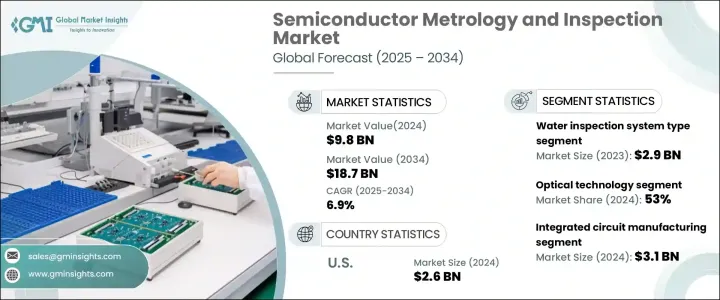
世界の半導体計測および検査市場は、2024年に98億米ドルと評価され、2025年から2034年にかけてCAGR 6.9%で拡大すると予測されています。
半導体製造プロセスの急速な進化と高性能チップへの需要の高まりが、市場を牽引しています。チップの設計が複雑化し、トランジスタのサイズが小さくなるにつれて、メーカーは精度と信頼性の確保という課題に直面しています。このため、ナノメートルスケールの精度で欠陥を検出できる高度な計測・検査システムへの需要が高まっています。自動車、家電、通信などの業界は、高い生産歩留まりを維持し、製造におけるコストのかかるエラーを最小限に抑えるため、こうしたソリューションに大きく依存しています。
特にサプライチェーンの混乱や地政学的要因に対応した半導体製造への世界の投資の急増が、市場の成長を後押ししています。世界中の政府および民間企業が半導体製造施設を拡張しており、精密な計測・検査システムへの差し迫ったニーズが生まれています。AI、IoT、5G技術の台頭は半導体部品の需要をさらに増大させ、厳格な品質管理対策を必要としています。さらに、業界が先端チップ製造のための極端紫外線(EUV)リソグラフィにシフトするにつれて、原子スケールで測定できる計測ツールの必要性がこれまで以上に高まっています。
| 市場範囲 | |
|---|---|
| 開始年 | 2024 |
| 予測年 | 2025-2034 |
| 開始金額 | 98億米ドル |
| 予測金額 | 187億米ドル |
| CAGR | 6.9% |
半導体計測および検査市場には、ウエハー検査システム、マスク検査システム、バンプ検査、薄膜計測、リードフレーム検査など、さまざまなカテゴリーが含まれます。2023年には、ウエハー検査システムが29億米ドルと大きなシェアを占めています。これらのシステムは、半導体ウエハー上の物理的欠陥とパターン欠陥の両方を特定する上で重要な役割を果たしています。正確な座標を取得することで、メーカーは汚染物質によるランダム欠陥と、露光やマスク条件に関連するシステマティック欠陥を区別することができます。欠陥を高精度で検出する能力は、生産効率の最適化と半導体デバイスの品質向上に不可欠です。
市場は技術別にも区分され、光学、電子ビーム、その他の先端技術がこの分野をリードしています。光学技術は2024年に53%のシェアを確保し、市場を独占すると予想されています。ナノメートルの精度で集積回路や半導体ウエハーを測定・分析できるためウエハーは広く採用されており、光学計測ソリューションはリソグラフィ工程での適切なアライメントを保証します。微細な欠陥をとらえるその能力は、精度が最も重要視される現代の半導体製造において不可欠なものとなっています。
ドイツの半導体計測および検査市場は、2034年までに11億米ドルに達すると予測されています。世界の半導体サプライチェーンの主要プレーヤーとして、ドイツは先進的な製造ソリューションに多額の投資を続けています。自動車、産業、家電産業における同国のリーダーシップが、高精度計測ツールの需要を促進しています。地元鋳造所の事業拡大に伴い、ウエハー製造と先進パッケージングをサポートする高度な計測・検査システムのニーズが大幅に高まることが予想されます。
目次
第1章 調査手法と調査範囲
- 市場範囲と定義
- 基本推定と計算
- 予測計算
- データソース
第2章 エグゼクティブサマリー
第3章 業界洞察
- エコシステム分析
- バリューチェーンに影響を与える要因
- 利益率分析
- 破壊
- 将来の展望
- メーカー
- 流通業者
- サプライヤーの状況
- 利益率分析
- 主要ニュース
- 規制状況
- 影響要因
- 促進要因
- 半導体デバイスの複雑化
- リソグラフィ技術の進歩
- 家電需要の増加
- IoTおよび5G対応デバイスの需要増加
- 半導体製造への投資の増加
- 業界の潜在的リスク&課題
- 先端装置の高コスト
- 既存システムとの統合問題
- 促進要因
- 成長可能性分析
- ポーター分析
- PESTEL分析
第4章 競合情勢
- イントロダクション
- 企業シェア分析
- 競合のポジショニング・マトリックス
- 戦略展望マトリックス
第5章 市場推計・予測:タイプ別、2021年~2034年
- 主要動向
- ウエハー検査装置
- マスク検査装置
- 薄膜検査装置
- バンプ検査
- リードフレーム検査
第6章 市場推計・予測:技術別、2021年~2034年
- 主要動向
- 光学
- 電子ビーム
- その他
第7章 市場推計・予測:用途別、2021年~2034年
- 主要動向
- 集積回路製造
- 発光ダイオード(LED)製造
- ディスクリートデバイス
- パッケージング・組立
- その他
第8章 市場推計・予測:最終用途別、2021年~2034年
- 主要動向
- 半導体鋳造メーカー
- 集積デバイスメーカー(IDM)
- サードパーティ・ビジネス(OSAT)
- 研究開発(R&D)機関
第9章 市場推計・予測:地域別、2021年~2034年
- 主要動向
- 北米
- 米国
- カナダ
- 欧州
- 英国
- ドイツ
- フランス
- イタリア
- スペイン
- ロシア
- アジア太平洋
- 中国
- インド
- 日本
- 韓国
- オーストラリア
- ラテンアメリカ
- ブラジル
- メキシコ
- 中東・アフリカ
- 南アフリカ
- サウジアラビア
- アラブ首長国連邦
第10章 企業プロファイル
- Advantest Corporation
- Applied Materials, Inc.
- ASML Holding N.V
- Bruker Corporation
- Camtek Ltd.
- Hitachi Ltd.
- JEOL Ltd.
- KLA Corporation
- Lasertec Corporation
- Nikon Corporation
- Nova Measuring Instruments Ltd.
- Olympus(EVIDENT)
- Onto Innovation, Inc
- Park Systems Corp.
- Thermo Fisher Scientific Inc.
- Toray Engineering Co., Ltd.
- Zygo Corporation
The Global Semiconductor Metrology And Inspection Market was valued at USD 9.8 billion in 2024 and is projected to expand at a CAGR of 6.9% from 2025 to 2034. The rapid evolution of semiconductor manufacturing processes, coupled with the growing demand for high-performance chips, is driving the market forward. As chip designs become more complex and transistor sizes shrink, manufacturers face increasing challenges in ensuring precision and reliability. This has led to a heightened demand for advanced metrology and inspection systems that can detect defects at nanometer-scale accuracy. Industries such as automotive, consumer electronics, and telecommunications rely heavily on these solutions to maintain high production yields and minimize costly errors in fabrication.
A surge in global investments in semiconductor manufacturing, particularly in response to supply chain disruptions and geopolitical factors, is fueling market growth. Governments and private enterprises worldwide are expanding semiconductor fabrication facilities, creating a pressing need for precise metrology and inspection systems. The rise of AI, IoT, and 5G technologies further amplifies the demand for semiconductor components, necessitating stringent quality control measures. Additionally, as the industry shifts toward extreme ultraviolet (EUV) lithography for advanced chip production, the need for metrology tools capable of measuring at the atomic scale is more critical than ever.
| Market Scope | |
|---|---|
| Start Year | 2024 |
| Forecast Year | 2025-2034 |
| Start Value | $9.8 Billion |
| Forecast Value | $18.7 Billion |
| CAGR | 6.9% |
The semiconductor metrology and inspection market encompasses various categories, including wafer inspection systems, mask inspection systems, bump inspection, thin film metrology, and lead frame inspection. In 2023, wafer inspection systems accounted for a substantial share, valued at USD 2.9 billion. These systems play a crucial role in identifying both physical and pattern defects on semiconductor wafers. By capturing precise coordinates, manufacturers can differentiate between random defects caused by contaminants and systematic defects related to exposure or mask conditions. The ability to detect defects with high precision is essential for optimizing production efficiency and enhancing the quality of semiconductor devices.
The market is also segmented based on technology, with optical, E-beam, and other advanced technologies leading the space. Optical technology is anticipated to dominate the market in 2024, securing a 53% share. Widely adopted due to its ability to measure and analyze integrated circuits and semiconductor wafers with nanometer accuracy, optical metrology solutions ensure proper alignment during the lithography process. Their capability to capture minute defects makes them indispensable in modern semiconductor manufacturing, where precision is paramount.
Germany semiconductor metrology and inspection market is projected to reach USD 1.1 billion by 2034. As a key player in the global semiconductor supply chain, Germany continues to invest heavily in advanced manufacturing solutions. The country's leadership in automotive, industrial, and consumer electronics industries is fueling the demand for high-precision metrology tools. With local foundries expanding operations, the need for sophisticated metrology and inspection systems to support wafer fabrication and advanced packaging is expected to rise significantly.
Table of Contents
Chapter 1 Methodology & Scope
- 1.1 Market scope & definitions
- 1.2 Base estimates & calculations
- 1.3 Forecast calculations
- 1.4 Data sources
- 1.4.1 Primary
- 1.4.2 Secondary
- 1.4.2.1 Paid sources
- 1.4.2.2 Public sources
Chapter 2 Executive Summary
- 2.1 Industry synopsis, 2021-2034
Chapter 3 Industry Insights
- 3.1 Industry ecosystem analysis
- 3.1.1 Factor affecting the value chain
- 3.1.2 Profit margin analysis
- 3.1.3 Disruptions
- 3.1.4 Future outlook
- 3.1.5 Manufacturers
- 3.1.6 Distributors
- 3.2 Supplier landscape
- 3.3 Profit margin analysis
- 3.4 Key news & initiatives
- 3.5 Regulatory landscape
- 3.6 Impact forces
- 3.6.1 Growth drivers
- 3.6.1.1 Increasing complexity of semiconductor devices
- 3.6.1.2 Advancements in lithography technologies
- 3.6.1.3 Rising consumer electronics demand
- 3.6.1.4 Rising demand for IoT and 5G-enabled devices
- 3.6.1.5 Increased investment in semiconductor manufacturing
- 3.6.2 Industry pitfalls & challenges
- 3.6.2.1 High cost of advanced equipment
- 3.6.2.2 Integration issues with existing systems
- 3.6.1 Growth drivers
- 3.7 Growth potential analysis
- 3.8 Porter's analysis
- 3.9 PESTEL analysis
Chapter 4 Competitive Landscape, 2024
- 4.1 Introduction
- 4.2 Company market share analysis
- 4.3 Competitive positioning matrix
- 4.4 Strategic outlook matrix
Chapter 5 Market Estimates & Forecast, By Type, 2021-2034 (USD Million)
- 5.1 Key trends
- 5.2 Wafer inspection system
- 5.3 Mask inspection system
- 5.4 Thin film metrology
- 5.5 Bump inspection
- 5.6 Lead frame inspection
Chapter 6 Market Estimates & Forecast, By Technology, 2021-2034 (USD Million)
- 6.1 Key trends
- 6.2 Optical
- 6.3 E-beam
- 6.4 Others
Chapter 7 Market Estimates & Forecast, By Application, 2021-2034 (USD Million)
- 7.1 Key trends
- 7.2 Integrated circuit manufacturing
- 7.3 Light Emitting Diode (LED) manufacturing
- 7.4 Discrete devices
- 7.5 Packaging and assembly
- 7.6 Others
Chapter 8 Market Estimates & Forecast, By End Use, 2021-2034 (USD Million)
- 8.1 Key trends
- 8.2 Semiconductor foundries
- 8.3 Integrated Device Manufacturers (IDMs)
- 8.4 Third-Party Business (OSAT)
- 8.5 Research & Development (R&D) institutions
Chapter 9 Market Estimates & Forecast, By Region, 2021-2034 (USD Million)
- 9.1 Key trends
- 9.2 North America
- 9.2.1 U.S.
- 9.2.2 Canada
- 9.3 Europe
- 9.3.1 UK
- 9.3.2 Germany
- 9.3.3 France
- 9.3.4 Italy
- 9.3.5 Spain
- 9.3.6 Russia
- 9.4 Asia Pacific
- 9.4.1 China
- 9.4.2 India
- 9.4.3 Japan
- 9.4.4 South Korea
- 9.4.5 Australia
- 9.5 Latin America
- 9.5.1 Brazil
- 9.5.2 Mexico
- 9.6 MEA
- 9.6.1 South Africa
- 9.6.2 Saudi Arabia
- 9.6.3 UAE
Chapter 10 Company Profiles
- 10.1 Advantest Corporation
- 10.2 Applied Materials, Inc.
- 10.3 ASML Holding N.V
- 10.4 Bruker Corporation
- 10.5 Camtek Ltd.
- 10.6 Hitachi Ltd.
- 10.7 JEOL Ltd.
- 10.8 KLA Corporation
- 10.9 Lasertec Corporation
- 10.10 Nikon Corporation
- 10.11 Nova Measuring Instruments Ltd.
- 10.12 Olympus (EVIDENT)
- 10.13 Onto Innovation, Inc
- 10.14 Park Systems Corp.
- 10.15 Thermo Fisher Scientific Inc.
- 10.16 Toray Engineering Co., Ltd.
- 10.17 Zygo Corporation

