|
|
市場調査レポート
商品コード
1290393
EUVリソグラフィの世界市場-2023-2030Global EUV Lithography Market - 2023-2030 |
||||||
カスタマイズ可能
適宜更新あり
|
|||||||
| EUVリソグラフィの世界市場-2023-2030 |
|
出版日: 2023年06月12日
発行: DataM Intelligence
ページ情報: 英文 182 Pages
納期: 即日から翌営業日
|
- 全表示
- 概要
- 目次
市場概要
EUVリソグラフィの世界市場規模は2022年に57億1,000万米ドルに達し、2023年から2030年の予測期間中に22.6%のCAGRで成長し、2030年には291億4,000万米ドルに達すると予測されています。
世界のEUVリソグラフィ市場は、技術の進歩、メモリやロジックデバイスの採用拡大、協業やパートナーシップ、AIや機械学習の統合、地理的拡大戦略などを背景に、急速な市場成長を遂げています。前述の市場動向は、半導体製造の状況を再構築し、先進的で効率的なリソグラフィプロセスだけでなく、より多くの市場機会の開拓を後押ししています。業界が進化を続ける中、これらの動向を先取りし、新たな市場機会を捉える企業は、EUVリソグラフィ市場の成長と変革から利益を得ることができます。
EUVリソグラフィの世界市場は、レーザー生成プラズマEUVリソグラフィ分野の大幅な拡大により、世界規模で半導体需要の急増が見られ、アプリケーション分野では市場シェアの3分の1以上を占めると予想されます。また、北米は市場シェアの5分の2以上を占め、支配的な地域となっています。
市場力学
技術的進歩と政府による支援政策
EUVリソグラフィ技術の継続的な進歩は、市場の成長を促進する上で極めて重要な役割を担っています。世界各国の政府は、リソグラフィシステム強化のための研究開発への投資の重要性を認識しています。世界各国の政府は、半導体産業を育成することの重要性を認識し、その発展を支援するための政策を実施しています。例えば、国内半導体メーカーの研究、技術革新、EUVリソグラフィ技術の採用を促進するために、税制上の優遇措置、補助金、助成金が提供されていることが統計で明らかになっています。このように、技術の進歩と政府の支援政策は、世界のEUVリソグラフィ市場の需要および市場機会を促進する主要な要因となっています。
規制と安全への懸念、歩留まりの課題、信頼性
EUVリソグラフィ技術の利用には、極端な紫外線の危険な性質に起因する厳しい安全プロトコルの遵守が必要です。世界各国の政府は、労働者と環境の安全を確保するために厳しい規制とガイドラインを課しています。これらの規制を遵守するためには、安全対策、従業員教育、監視システムへの追加投資が必要であり、市場の成長を阻害しています。公式な報告によると、EUVリソグラフィ業界では、規制遵守が全体的な運用コストのかなりの部分を占めているとのことです。
さらに、EUVリソグラフィの導入は、高い生産歩留まりを達成する上で新たな課題をもたらします。この技術は、マスクや光源の微細な欠陥に敏感であるため、製造工程で歩留まりが低下してしまうのです。業界では、半導体メーカーの厳しい要求に応えるため、信頼性と歩留まりの向上に努めていますが、依然として継続的な課題となっています。歩留まり改善への取り組みは、研究開発への多額の投資を必要とし、メーカーの総コストを押し上げています。
目次
第1章 調査手法とスコープ
- 調査手法
- 調査目的および調査範囲
第2章 定義と概要
第3章 エグゼクティブサマリー
第4章 市場力学
- 影響要因
- 促進要因
- 小型化ニーズの高まりとそれに伴う先端半導体デバイスの需要増
- 技術革新と政府による支援政策
- 抑制要因
- 技術的な複雑さ、法外なコスト、主要コンポーネントの入手制限
- 規制と安全性への懸念、歩留まりの問題、信頼性
- 機会
- 影響分析
- 促進要因
第5章 産業分析
- ポーターのファイブフォース分析
- サプライチェーン分析
- 価格分析
- 法規制の分析
第6章 COVID-19の分析
第7章 光源別
- レーザー生成プラズマ(LPP)
- 真空スパーク
- ガス放電
第8章 アプリケーション別
- 総合半導体企業(IDM)
- ファウンドリ
第9章 装置別
- 光源
- ミラー
- マスク
- その他
第10章 地域別
- 北米
- 米国
- カナダ
- メキシコ
- 欧州
- ドイツ
- 英国
- フランス
- イタリア
- ロシア
- その他欧州
- 南米
- ブラジル
- アルゼンチン
- その他南米地域
- アジア太平洋地域
- 中国
- インド
- 日本
- オーストラリア
- その他アジア太平洋地域
- 中東・アフリカ地域
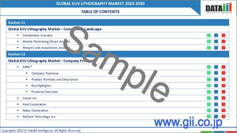
第11章 競合情勢
- 競合シナリオ
- 市況ポジショニング/シェア分析
- M&A(合併・買収)分析
第12章 企業プロファイル
- ASML
- 会社概要
- 製品ポートフォリオと説明
- 財務概要
- 主な発展状況
- Canon Inc.
- Intel Corporation
- Nikon Corporation
- NuFlare Technology Inc.
- Samsung Corporation
- SUSS Microtec AG
- Taiwan Semiconductor Manufacturing Company Limited(TSMC)
- Ultratech Inc.
- Vistec Semiconductor Systems
第13章 付録
Market Overview
The Global EUV Lithography Market size reached US$ 5.71 billion in 2022 and is expected to reach US$ 29.14 billion by 2030 growing at a CAGR of 22.6% during the forecast period 2023-2030.
The global EUV lithography market is experiencing rapid market growth, fueled by technological advancements, increasing adoption of memory and logic devices, collaborations and partnerships, the integration of AI and machine learning, and geographical expansion strategies. The aforementioned market trends are reshaping the semiconductor manufacturing landscape, driving the development of more market opportunities as well as advanced and efficient lithography processes. As the industry continues to evolve, businesses that stay ahead of these trends and seize emerging market opportunities stand to benefit from the growth and transformation of the EUV lithography market.
The global EUV lithography market is witnessing a surge in demand for semiconductors on a global scale due to significant expansion in the laser-produced plasma EUV lithography segment, which is anticipated to capture more than one-third of the market share within the application segment. Likewise, North America emerges as a dominant region, accounting for over two-fifths of the market share.
Market Dynamics
Technological Advancements and Supportive Government Policies
Continuous advancements in EUV lithography technology have played a pivotal role in driving market growth. Governments worldwide have acknowledged the importance of investing in research and development to enhance lithography systems. Governments worldwide have recognized the importance of nurturing the semiconductor industry and have implemented policies to support its development. For example, statistics reveal the provision of tax incentives, grants, and subsidies to encourage research, innovation, and the adoption of EUV lithography technology by domestic semiconductor manufacturers. Thus, technological advancements and supportive government policies act as major drivers for demand and market opportunities in the global EUV lithography market.
Regulatory and Safety Concerns, Yield Challenges and Reliability
The utilization of EUV lithography technology necessitates adherence to stringent safety protocols due to the hazardous nature of extreme ultraviolet radiation. Governments across the globe impose strict regulations and guidelines to ensure the safety of workers and the environment. Compliance with these regulations requires additional investments in safety measures, employee training, and monitoring systems, thereby impeding the market's growth. Official reports indicate that regulatory compliance accounts for a significant portion of the overall operational costs in the EUV lithography industry.
Furthermore, the implementation of EUV lithography introduces new challenges in achieving high production yields. The technology's sensitivity to minute defects in masks and light sources results in yield loss during the manufacturing process. The industry is striving to improve reliability and yield rates to meet the stringent requirements of semiconductor manufacturers, but it remains an ongoing challenge. Yield improvement initiatives require substantial investments in research and development, driving up the overall costs for manufacturers.
Segment Analysis
The global automotive oem coatings market is segmented based on light source, application, equipment and region.
Growing Semiconductor Demand, Advancement In Technology And Increase In Government Funding
The Laser Produced Plasma (LPP) segment has emerged as a critical component within the global EUV lithography market. By utilizing high-powered lasers, LPP technology generates extreme ultraviolet light, enabling the creation of more advanced semiconductor chips. Governmental statistics demonstrate the growing emphasis on LPP technology and its positive impact on the semiconductor industries of various countries.
The European Union (EU), for instance, has placed a strong emphasis on promoting advanced semiconductor manufacturing within its borders. In recent years, the EU has allocated significant funding to research projects focusing on LPP technology, aiming to strengthen its position in the global EUV lithography market. Furthermore, countries such as the U.S., Japan, South Korea, and Taiwan have also prioritized the advancement of LPP technology within their semiconductor industries.
Through strategic partnerships between governments, research institutions, and industry players, these nations have sought to enhance their competitiveness in the global market, fostering the growth of the LPP segment. As governments continue to support research and development in LPP technology and manufacturers drive further innovations, the LPP segment is poised for sustained growth. The aforementioned factors will play a pivotal role in advancing the semiconductor industry, enabling the production of smaller, more powerful, and more efficient electronic devices in the future.
Geographical Analysis
Governmental Support and Technological Advancements in North America
The North America region demonstrates a prominent presence in the global EUV lithography market, fueled by governmental support, technological advancements, and notable product launches. The U.S. and Canada, in particular, have witnessed positive growth in the semiconductor industry, leading to increased adoption of EUV lithography technology. For instance, Canada's semiconductor industry has experienced substantial growth in recent years, contributing to the North America region's EUV lithography market.
The Canadian government has actively supported the development of the semiconductor sector, emphasizing innovation and technological advancement. According to Statistics Canada, the manufacturing sales of electronic and electrical equipment, including semiconductors, increased by 8.5% in 2021, reflecting the industry's positive momentum. As the region continues to invest in research and development, it is expected to maintain its significant role in the global EUV lithography market, contributing to the advancement of the semiconductor industry as a whole.
Competitive Landscape
The major global players in the market include: ASML, Canon Inc., Intel Corporation, Nikon Corporation, NuFlare Technology Inc., Samsung Corporation, SUSS Microtec AG, Taiwan Semiconductor Manufacturing Company Limited (TSMC), Ultratech Inc. and Vistec Semiconductor Systems.
Why Purchase the Report?
- To visualize the global EUV lithography market segmentation based on light source, application, equipment and region, as well as understand key commercial assets and players.
- Identify commercial opportunities by analyzing trends and co-development.
- Excel data sheet with numerous data points of EUV lithography market-level with all segments.
- PDF report consists of a comprehensive analysis after exhaustive qualitative interviews and an in-depth study.
- Product mapping available as Excel consisting of key products of all the major players.
The global EUV lithography market report would provide approximately 61 tables, 57 figures and 182 pages.
Target Audience 2023
- Manufacturers/ Buyers
- Industry Investors/Investment Bankers
- Research Professionals
- Emerging Companies
Table of Contents
1. Methodology and Scope
- 1.1. Research Methodology
- 1.2. Research Objective and Scope of the Report
2. Definition and Overview
3. Executive Summary
- 3.1. Snippet by Light Source
- 3.2. Snippet by Application
- 3.3. Snippet by Equipment
- 3.4. Snippet by Region
4. Dynamics
- 4.1. Impacting Factors
- 4.1.1. Drivers
- 4.1.1.1. Rising Need for Miniaturization and Associated Increase in Demand for Advanced Semiconductor Devices
- 4.1.1.2. Technological Advancements and Supportive Government Policies
- 4.1.2. Restraints
- 4.1.2.1. Technological Complexity, Exorbitant Cost and Limited Availability of Key Components
- 4.1.2.2. Regulatory and Safety Concerns, Yield Challenges and Reliability
- 4.1.3. Opportunity
- 4.1.4. Impact Analysis
- 4.1.1. Drivers
5. Industry Analysis
- 5.1. Porter's Five Force Analysis
- 5.2. Supply Chain Analysis
- 5.3. Pricing Analysis
- 5.4. Regulatory Analysis
6. COVID-19 Analysis
- 6.1. Analysis of COVID-19
- 6.1.1. Scenario Before COVID
- 6.1.2. Scenario During COVID
- 6.1.3. Scenario Post COVID
- 6.2. Pricing Dynamics Amid COVID-19
- 6.3. Demand-Supply Spectrum
- 6.4. Government Initiatives Related to the Market During Pandemic
- 6.5. Manufacturers Strategic Initiatives
- 6.6. Conclusion
7. By Light Source
- 7.1. Introduction
- 7.1.1. Market Size Analysis and Y-o-Y Growth Analysis (%), By Light Source
- 7.1.2. Market Attractiveness Index, By Light Source
- 7.2. Laser Produced Plasma (LPP)*
- 7.2.1. Introduction
- 7.2.2. Market Size Analysis and Y-o-Y Growth Analysis (%)
- 7.3. Vacuum Sparks
- 7.4. Gas Discharges
8. By Application
- 8.1. Introduction
- 8.1.1. Market Size Analysis and Y-o-Y Growth Analysis (%), By Application
- 8.1.2. Market Attractiveness Index, By Application
- 8.2. Integrated Device Manufacturer (IDM)*
- 8.2.1. Introduction
- 8.2.2. Market Size Analysis and Y-o-Y Growth Analysis (%)
- 8.3. Foundry
9. By Equipment
- 9.1. Introduction
- 9.1.1. Market Size Analysis and Y-o-Y Growth Analysis (%), By Equipment
- 9.1.2. Market Attractiveness Index, By Equipment
- 9.2. Light Source*
- 9.2.1. Introduction
- 9.2.2. Market Size Analysis and Y-o-Y Growth Analysis (%)
- 9.3. Mirrors
- 9.4. Masks
- 9.5. Others
10. By Region
- 10.1. Introduction
- 10.1.1. Market Size Analysis and Y-o-Y Growth Analysis (%), By Region
- 10.1.2. Market Attractiveness Index, By Region
- 10.2. North America
- 10.2.1. Introduction
- 10.2.2. Key Region-Specific Dynamics
- 10.2.3. Market Size Analysis and Y-o-Y Growth Analysis (%), By Light Source
- 10.2.4. Market Size Analysis and Y-o-Y Growth Analysis (%), By Application
- 10.2.5. Market Size Analysis and Y-o-Y Growth Analysis (%), By Equipment
- 10.2.6. Market Size Analysis and Y-o-Y Growth Analysis (%), By Country
- 10.2.6.1. The U.S.
- 10.2.6.2. Canada
- 10.2.6.3. Mexico
- 10.3. Europe
- 10.3.1. Introduction
- 10.3.2. Key Region-Specific Dynamics
- 10.3.3. Market Size Analysis and Y-o-Y Growth Analysis (%), By Light Source
- 10.3.4. Market Size Analysis and Y-o-Y Growth Analysis (%), By Application
- 10.3.5. Market Size Analysis and Y-o-Y Growth Analysis (%), By Equipment
- 10.3.6. Market Size Analysis and Y-o-Y Growth Analysis (%), By Country
- 10.3.6.1. Germany
- 10.3.6.2. The UK
- 10.3.6.3. France
- 10.3.6.4. Italy
- 10.3.6.5. Russia
- 10.3.6.6. Rest of Europe
- 10.4. South America
- 10.4.1. Introduction
- 10.4.2. Key Region-Specific Dynamics
- 10.4.3. Market Size Analysis and Y-o-Y Growth Analysis (%), By Light Source
- 10.4.4. Market Size Analysis and Y-o-Y Growth Analysis (%), By Application
- 10.4.5. Market Size Analysis and Y-o-Y Growth Analysis (%), By Equipment
- 10.4.6. Market Size Analysis and Y-o-Y Growth Analysis (%), By Country
- 10.4.6.1. Brazil
- 10.4.6.2. Argentina
- 10.4.6.3. Rest of South America
- 10.5. Asia-Pacific
- 10.5.1. Introduction
- 10.5.2. Key Region-Specific Dynamics
- 10.5.3. Market Size Analysis and Y-o-Y Growth Analysis (%), By Light Source
- 10.5.4. Market Size Analysis and Y-o-Y Growth Analysis (%), By Application
- 10.5.5. Market Size Analysis and Y-o-Y Growth Analysis (%), By Equipment
- 10.5.6. Market Size Analysis and Y-o-Y Growth Analysis (%), By Country
- 10.5.6.1. China
- 10.5.6.2. India
- 10.5.6.3. Japan
- 10.5.6.4. Australia
- 10.5.6.5. Rest of Asia-Pacific
- 10.6. Middle East and Africa
- 10.6.1. Introduction
- 10.6.2. Key Region-Specific Dynamics
- 10.6.3. Market Size Analysis and Y-o-Y Growth Analysis (%), By Light Source
- 10.6.4. Market Size Analysis and Y-o-Y Growth Analysis (%), By Application
- 10.6.5. Market Size Analysis and Y-o-Y Growth Analysis (%), By Equipment
11. Competitive Landscape
- 11.1. Competitive Scenario
- 11.2. Market Positioning/Share Analysis
- 11.3. Mergers and Acquisitions Analysis
12. Company Profiles
- 12.1. ASML*
- 12.1.1. Company Overview
- 12.1.2. Product Portfolio and Description
- 12.1.3. Financial Overview
- 12.1.4. Key Developments
- 12.2. Canon Inc.
- 12.3. Intel Corporation
- 12.4. Nikon Corporation
- 12.5. NuFlare Technology Inc.
- 12.6. Samsung Corporation
- 12.7. SUSS Microtec AG
- 12.8. Taiwan Semiconductor Manufacturing Company Limited (TSMC)
- 12.9. Ultratech Inc.
- 12.10. Vistec Semiconductor Systems
LIST NOT EXHAUSTIVE
13. Appendix
- 13.1. About Us and Services
- 13.2. Contact Us
