|
|
市場調査レポート
商品コード
1423604
半導体検査・測定装置の2030年までの世界市場予測: タイプ別、機能別、技術別、用途別、地域別の世界分析Semiconductor Inspection and Measurement Equipment Market Forecasts to 2030 - Global Analysis By Type, Function, Technology, Application and By Geography |
||||||
|
|||||||
カスタマイズ可能
|
|||||||

| 半導体検査・測定装置の2030年までの世界市場予測: タイプ別、機能別、技術別、用途別、地域別の世界分析 |
|
出版日: 2024年02月02日
発行: Stratistics Market Research Consulting
ページ情報: 英文 200+ Pages
納期: 2~3営業日
|

全表示
- 概要
- 図表
- 目次
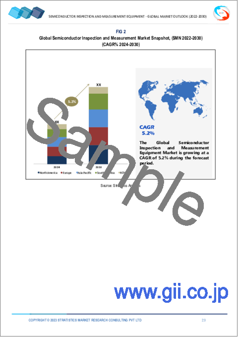
Stratistics MRCによると、半導体検査・測定装置の世界市場は予測期間中CAGR 5.2%で成長します。
半導体検査・測定装置は、半導体デバイス、チップ、集積回路(IC)の品質、精度、信頼性を確保するために、半導体製造工程で使用される特殊なツールとシステムのセットです。これらのツールは、ウエハー検査、欠陥検出、計測(寸法や特性の測定)、プロセス制御など、半導体製造のさまざまな段階で重要な役割を果たしています。
SEMIによると、2022年の世界のシリコンウエハー出荷面積は147億1,000万平方インチに達し、2021年の141億6,000万平方インチから増加しました。
半導体需要の増加
IoT、5G、AI、電気自動車などの技術の急速な普及によって、半導体需要が急増しており、精密で高品質な半導体チップの必要性が高まっています。この急増により、厳格な品質管理を保証し、欠陥を検出し、製造プロセスを最適化するための高度な検査・測定装置が必要となります。各業界が半導体対応技術に大きく依存する中、信頼性が高く効率的な検査・計測機器への需要が高まり、半導体検査・計測機器市場の成長を牽引しています。
装置の高コスト
半導体検査・測定装置は、その洗練された技術、精度要件、進化する製造標準に合わせるための頻繁なアップグレードの必要性から、多額の投資が必要となります。この経済的負担は、特に小規模メーカーや予算が限られているメーカーにとっては、最先端機器を入手する能力を制限し、アクセス性を阻害する可能性があります。その結果、手頃な価格が課題となり、半導体業界における競争力の妨げとなっています。
高性能半導体チップへの需要の高まり
技術の進歩により、AI、高速コンピューティング、通信などのアプリケーション向けに、より高速で高性能なチップの必要性が高まるにつれ、精密で信頼性の高い検査ツールへの要求も高まっています。この需要は、厳格な品質管理を保証し、欠陥を検出し、これらの高性能チップ上の複雑な機能を検証することができる高度な装置を必要とします。その結果、最先端の半導体デバイスを製造するための進化する要件を満たすために、高度な検査・測定ソリューションへの技術革新と投資が促進され、市場の成長と開拓が促進されます。
環境への配慮
このような高度なツールの製造工程では、有害物質の使用やエネルギー集約的な手順が多く、環境への影響が懸念されます。廃棄物処理、エネルギー消費、有害物質に関する厳しい規制を遵守するためには、環境に優しい製造方法に多額の投資を行う必要があります。こうした懸念に対処できなければ、操業コストの増大、市場受容の制限、規制の不遵守を招き、成長と市場の妨げになる可能性があります。
COVID-19の影響
COVID-19の大流行は当初、サプライチェーンの混乱、生産の停滞、設備納入の遅れを引き起こしました。しかし、リモートワークの急増、デジタル化、電子機器に対する需要の増加により、半導体チップの要件が高まった。その結果、品質基準を維持するための検査・測定機器のニーズが高まった。全体として、課題に直面しながらも、パンデミックは半導体デバイスの長期的な需要に拍車をかけ、検査・計測機器市場の継続的な成長を促進しました。
予測期間中、計測機器セグメントが最大になる見込み
計測機器分野が最大のシェアを占めると推定されます。計測機器は、重要な寸法、表面形状、膜厚、その他の特性をナノメートルスケールで測定することにより、半導体部品や材料の品質、精度、適合性を保証します。さらに、計測機器は、光学、走査型電子顕微鏡(SEM)、原子間力顕微鏡(AFM)などの先端技術を採用し、半導体の特徴を徹底的に検査・検証することで、製造プロセス全体を通じて設計仕様や高品質基準の順守を保証します。
予測期間中、ウエハーセグメンテーションのCAGRが最も高くなると予想されます。
ウエハー分野は、予測期間中に有利な成長を遂げると予想されています。ウエハーとは、シリコンのような半導体材料でできた薄い円盤状の基板のことです。このウエハは、集積回路(IC)やマイクロチップを製造するための基盤材料として機能します。ウエハー検査・測定装置には、これらのウエハーの品質、均一性、欠陥、重要なパラメータを検査・評価するために設計された特殊なツールやシステムが含まれます。さらに、これらのツールは、半導体製造プロセスを通じてウエハーの完全性、精度、信頼性を確保し、チップの歩留まりと性能を最適化するために極めて重要です。
最大シェアの地域
アジア太平洋地域は、半導体製造における優位性により、予測期間中に最大の市場シェアを占めました。この地域の成長は、技術の進歩、民生用電子機器の需要増加、急速な工業化によって推進されています。ASML、東京エレクトロン、地元企業を含むこの地域の企業は、最先端の検査・計測装置に対するニーズの高まりに対応するために積極的に技術革新を行っており、アジア太平洋地域の半導体産業における重要な市場促進要因としての地位をさらに強固なものにしています。
CAGRが最も高い地域:
北米は、その技術革新と強固な半導体エコシステムにより、予測期間中に有益な成長を遂げると予想されます。米国は、主要な半導体メーカーやテクノロジー大手が集積しており、極めて重要な役割を果たしています。アプライドマテリアルズ、KLAコーポレーション、ナノメトリクスのような企業が、検査・計測ソリューションの進歩を先導しています。さらに、この地域の研究開発への注力は、高性能コンピューティング、人工知能、車載エレクトロニクスの需要増加と相まって、市場の成長を支えています。
無料のカスタマイズサービス:
本レポートをご購読のお客様には、以下の無料カスタマイズオプションのいずれかをご利用いただけます:
- 企業プロファイル
- 追加市場プレイヤーの包括的プロファイリング(3社まで)
- 主要企業のSWOT分析(3社まで)
- 地域セグメンテーション
- 顧客の関心に応じた主要国の市場推計・予測・CAGR(注:フィージビリティチェックによる)
- 競合ベンチマーキング
- 製品ポートフォリオ、地理的プレゼンス、戦略的提携に基づく主要企業のベンチマーキング
目次
第1章 エグゼクティブサマリー
第2章 序文
- 概要
- ステークホルダー
- 調査範囲
- 調査手法
- データマイニング
- データ分析
- データ検証
- 調査アプローチ
- 調査ソース
- 1次調査ソース
- 2次調査ソース
- 前提条件
第3章 市場動向分析
- 促進要因
- 抑制要因
- 機会
- 脅威
- 技術分析
- アプリケーション分析
- 新興市場
- 新型コロナウイルス感染症(COVID-19)の影響
第4章 ポーターのファイブフォース分析
- 供給企業の交渉力
- 買い手の交渉力
- 代替品の脅威
- 新規参入業者の脅威
- 競争企業間の敵対関係
第5章 世界の半導体検査・測定装置市場:タイプ別
- 計測機器
- 欠陥検査装置
第6章 世界の半導体検査・測定装置市場:機能別
- 自動検査システム
- 手動検査システム
- ソフトウェアソリューション
第7章 世界の半導体検査・測定装置市場:技術別
- 光学検査
- 走査型プローブ顕微鏡
- 電子線検査
- その他の技術
第8章 世界の半導体検査・測定装置市場:用途別
- マスク/フィルム
- ウエハー
- プロセス制御と最適化
- 研究開発
- その他の用途
第9章 世界の半導体検査・測定装置市場:地域別
- 北米
- 米国
- カナダ
- メキシコ
- 欧州
- ドイツ
- 英国
- イタリア
- フランス
- スペイン
- その他欧州
- アジア太平洋地域
- 日本
- 中国
- インド
- オーストラリア
- ニュージーランド
- 韓国
- その他アジア太平洋地域
- 南米
- アルゼンチン
- ブラジル
- チリ
- その他南米
- 中東とアフリカ
- サウジアラビア
- アラブ首長国連邦
- カタール
- 南アフリカ
- その他中東とアフリカ
第10章 主な発展
- 契約、パートナーシップ、コラボレーション、合弁事業
- 買収と合併
- 新製品の発売
- 事業拡大
- その他の主要戦略
第11章 企業プロファイル
- KLA Corporation
- Hitachi High-Technologies
- Applied Materials
- Onto Innovation
- ASML
- SCREEN Semiconductor Solutions
- Lasertec
- Camtek
- ZEISS
- Toray Engineering
- Unity Semiconductor SAS
- Microtronic
- RSIC
- Muetec
- DJEL
List of Tables
- Table 1 Global Semiconductor Inspection and Measurement Equipment Market Outlook, By Region (2021-2030) ($MN)
- Table 2 Global Semiconductor Inspection and Measurement Equipment Market Outlook, By Type (2021-2030) ($MN)
- Table 3 Global Semiconductor Inspection and Measurement Equipment Market Outlook, By Metrology Equipment (2021-2030) ($MN)
- Table 4 Global Semiconductor Inspection and Measurement Equipment Market Outlook, By Defect Inspection Equipment (2021-2030) ($MN)
- Table 5 Global Semiconductor Inspection and Measurement Equipment Market Outlook, By Function (2021-2030) ($MN)
- Table 6 Global Semiconductor Inspection and Measurement Equipment Market Outlook, By Automated Inspection Systems (2021-2030) ($MN)
- Table 7 Global Semiconductor Inspection and Measurement Equipment Market Outlook, By Manual Inspection Systems (2021-2030) ($MN)
- Table 8 Global Semiconductor Inspection and Measurement Equipment Market Outlook, By Software Solutions (2021-2030) ($MN)
- Table 9 Global Semiconductor Inspection and Measurement Equipment Market Outlook, By Technology (2021-2030) ($MN)
- Table 10 Global Semiconductor Inspection and Measurement Equipment Market Outlook, By Optical Inspection (2021-2030) ($MN)
- Table 11 Global Semiconductor Inspection and Measurement Equipment Market Outlook, By Scanning Probe Microscopy (2021-2030) ($MN)
- Table 12 Global Semiconductor Inspection and Measurement Equipment Market Outlook, By Electron Beam Inspection (2021-2030) ($MN)
- Table 13 Global Semiconductor Inspection and Measurement Equipment Market Outlook, By Other Technologies (2021-2030) ($MN)
- Table 14 Global Semiconductor Inspection and Measurement Equipment Market Outlook, By Application (2021-2030) ($MN)
- Table 15 Global Semiconductor Inspection and Measurement Equipment Market Outlook, By Mask/Film (2021-2030) ($MN)
- Table 16 Global Semiconductor Inspection and Measurement Equipment Market Outlook, By Wafer (2021-2030) ($MN)
- Table 17 Global Semiconductor Inspection and Measurement Equipment Market Outlook, By Process Control and Optimization (2021-2030) ($MN)
- Table 18 Global Semiconductor Inspection and Measurement Equipment Market Outlook, By Research and Development (2021-2030) ($MN)
- Table 19 Global Semiconductor Inspection and Measurement Equipment Market Outlook, By Other Applications (2021-2030) ($MN)
- Table 20 North America Semiconductor Inspection and Measurement Equipment Market Outlook, By Country (2021-2030) ($MN)
- Table 21 North America Semiconductor Inspection and Measurement Equipment Market Outlook, By Type (2021-2030) ($MN)
- Table 22 North America Semiconductor Inspection and Measurement Equipment Market Outlook, By Metrology Equipment (2021-2030) ($MN)
- Table 23 North America Semiconductor Inspection and Measurement Equipment Market Outlook, By Defect Inspection Equipment (2021-2030) ($MN)
- Table 24 North America Semiconductor Inspection and Measurement Equipment Market Outlook, By Function (2021-2030) ($MN)
- Table 25 North America Semiconductor Inspection and Measurement Equipment Market Outlook, By Automated Inspection Systems (2021-2030) ($MN)
- Table 26 North America Semiconductor Inspection and Measurement Equipment Market Outlook, By Manual Inspection Systems (2021-2030) ($MN)
- Table 27 North America Semiconductor Inspection and Measurement Equipment Market Outlook, By Software Solutions (2021-2030) ($MN)
- Table 28 North America Semiconductor Inspection and Measurement Equipment Market Outlook, By Technology (2021-2030) ($MN)
- Table 29 North America Semiconductor Inspection and Measurement Equipment Market Outlook, By Optical Inspection (2021-2030) ($MN)
- Table 30 North America Semiconductor Inspection and Measurement Equipment Market Outlook, By Scanning Probe Microscopy (2021-2030) ($MN)
- Table 31 North America Semiconductor Inspection and Measurement Equipment Market Outlook, By Electron Beam Inspection (2021-2030) ($MN)
- Table 32 North America Semiconductor Inspection and Measurement Equipment Market Outlook, By Other Technologies (2021-2030) ($MN)
- Table 33 North America Semiconductor Inspection and Measurement Equipment Market Outlook, By Application (2021-2030) ($MN)
- Table 34 North America Semiconductor Inspection and Measurement Equipment Market Outlook, By Mask/Film (2021-2030) ($MN)
- Table 35 North America Semiconductor Inspection and Measurement Equipment Market Outlook, By Wafer (2021-2030) ($MN)
- Table 36 North America Semiconductor Inspection and Measurement Equipment Market Outlook, By Process Control and Optimization (2021-2030) ($MN)
- Table 37 North America Semiconductor Inspection and Measurement Equipment Market Outlook, By Research and Development (2021-2030) ($MN)
- Table 38 North America Semiconductor Inspection and Measurement Equipment Market Outlook, By Other Applications (2021-2030) ($MN)
- Table 39 Europe Semiconductor Inspection and Measurement Equipment Market Outlook, By Country (2021-2030) ($MN)
- Table 40 Europe Semiconductor Inspection and Measurement Equipment Market Outlook, By Type (2021-2030) ($MN)
- Table 41 Europe Semiconductor Inspection and Measurement Equipment Market Outlook, By Metrology Equipment (2021-2030) ($MN)
- Table 42 Europe Semiconductor Inspection and Measurement Equipment Market Outlook, By Defect Inspection Equipment (2021-2030) ($MN)
- Table 43 Europe Semiconductor Inspection and Measurement Equipment Market Outlook, By Function (2021-2030) ($MN)
- Table 44 Europe Semiconductor Inspection and Measurement Equipment Market Outlook, By Automated Inspection Systems (2021-2030) ($MN)
- Table 45 Europe Semiconductor Inspection and Measurement Equipment Market Outlook, By Manual Inspection Systems (2021-2030) ($MN)
- Table 46 Europe Semiconductor Inspection and Measurement Equipment Market Outlook, By Software Solutions (2021-2030) ($MN)
- Table 47 Europe Semiconductor Inspection and Measurement Equipment Market Outlook, By Technology (2021-2030) ($MN)
- Table 48 Europe Semiconductor Inspection and Measurement Equipment Market Outlook, By Optical Inspection (2021-2030) ($MN)
- Table 49 Europe Semiconductor Inspection and Measurement Equipment Market Outlook, By Scanning Probe Microscopy (2021-2030) ($MN)
- Table 50 Europe Semiconductor Inspection and Measurement Equipment Market Outlook, By Electron Beam Inspection (2021-2030) ($MN)
- Table 51 Europe Semiconductor Inspection and Measurement Equipment Market Outlook, By Other Technologies (2021-2030) ($MN)
- Table 52 Europe Semiconductor Inspection and Measurement Equipment Market Outlook, By Application (2021-2030) ($MN)
- Table 53 Europe Semiconductor Inspection and Measurement Equipment Market Outlook, By Mask/Film (2021-2030) ($MN)
- Table 54 Europe Semiconductor Inspection and Measurement Equipment Market Outlook, By Wafer (2021-2030) ($MN)
- Table 55 Europe Semiconductor Inspection and Measurement Equipment Market Outlook, By Process Control and Optimization (2021-2030) ($MN)
- Table 56 Europe Semiconductor Inspection and Measurement Equipment Market Outlook, By Research and Development (2021-2030) ($MN)
- Table 57 Europe Semiconductor Inspection and Measurement Equipment Market Outlook, By Other Applications (2021-2030) ($MN)
- Table 58 Asia Pacific Semiconductor Inspection and Measurement Equipment Market Outlook, By Country (2021-2030) ($MN)
- Table 59 Asia Pacific Semiconductor Inspection and Measurement Equipment Market Outlook, By Type (2021-2030) ($MN)
- Table 60 Asia Pacific Semiconductor Inspection and Measurement Equipment Market Outlook, By Metrology Equipment (2021-2030) ($MN)
- Table 61 Asia Pacific Semiconductor Inspection and Measurement Equipment Market Outlook, By Defect Inspection Equipment (2021-2030) ($MN)
- Table 62 Asia Pacific Semiconductor Inspection and Measurement Equipment Market Outlook, By Function (2021-2030) ($MN)
- Table 63 Asia Pacific Semiconductor Inspection and Measurement Equipment Market Outlook, By Automated Inspection Systems (2021-2030) ($MN)
- Table 64 Asia Pacific Semiconductor Inspection and Measurement Equipment Market Outlook, By Manual Inspection Systems (2021-2030) ($MN)
- Table 65 Asia Pacific Semiconductor Inspection and Measurement Equipment Market Outlook, By Software Solutions (2021-2030) ($MN)
- Table 66 Asia Pacific Semiconductor Inspection and Measurement Equipment Market Outlook, By Technology (2021-2030) ($MN)
- Table 67 Asia Pacific Semiconductor Inspection and Measurement Equipment Market Outlook, By Optical Inspection (2021-2030) ($MN)
- Table 68 Asia Pacific Semiconductor Inspection and Measurement Equipment Market Outlook, By Scanning Probe Microscopy (2021-2030) ($MN)
- Table 69 Asia Pacific Semiconductor Inspection and Measurement Equipment Market Outlook, By Electron Beam Inspection (2021-2030) ($MN)
- Table 70 Asia Pacific Semiconductor Inspection and Measurement Equipment Market Outlook, By Other Technologies (2021-2030) ($MN)
- Table 71 Asia Pacific Semiconductor Inspection and Measurement Equipment Market Outlook, By Application (2021-2030) ($MN)
- Table 72 Asia Pacific Semiconductor Inspection and Measurement Equipment Market Outlook, By Mask/Film (2021-2030) ($MN)
- Table 73 Asia Pacific Semiconductor Inspection and Measurement Equipment Market Outlook, By Wafer (2021-2030) ($MN)
- Table 74 Asia Pacific Semiconductor Inspection and Measurement Equipment Market Outlook, By Process Control and Optimization (2021-2030) ($MN)
- Table 75 Asia Pacific Semiconductor Inspection and Measurement Equipment Market Outlook, By Research and Development (2021-2030) ($MN)
- Table 76 Asia Pacific Semiconductor Inspection and Measurement Equipment Market Outlook, By Other Applications (2021-2030) ($MN)
- Table 77 South America Semiconductor Inspection and Measurement Equipment Market Outlook, By Country (2021-2030) ($MN)
- Table 78 South America Semiconductor Inspection and Measurement Equipment Market Outlook, By Type (2021-2030) ($MN)
- Table 79 South America Semiconductor Inspection and Measurement Equipment Market Outlook, By Metrology Equipment (2021-2030) ($MN)
- Table 80 South America Semiconductor Inspection and Measurement Equipment Market Outlook, By Defect Inspection Equipment (2021-2030) ($MN)
- Table 81 South America Semiconductor Inspection and Measurement Equipment Market Outlook, By Function (2021-2030) ($MN)
- Table 82 South America Semiconductor Inspection and Measurement Equipment Market Outlook, By Automated Inspection Systems (2021-2030) ($MN)
- Table 83 South America Semiconductor Inspection and Measurement Equipment Market Outlook, By Manual Inspection Systems (2021-2030) ($MN)
- Table 84 South America Semiconductor Inspection and Measurement Equipment Market Outlook, By Software Solutions (2021-2030) ($MN)
- Table 85 South America Semiconductor Inspection and Measurement Equipment Market Outlook, By Technology (2021-2030) ($MN)
- Table 86 South America Semiconductor Inspection and Measurement Equipment Market Outlook, By Optical Inspection (2021-2030) ($MN)
- Table 87 South America Semiconductor Inspection and Measurement Equipment Market Outlook, By Scanning Probe Microscopy (2021-2030) ($MN)
- Table 88 South America Semiconductor Inspection and Measurement Equipment Market Outlook, By Electron Beam Inspection (2021-2030) ($MN)
- Table 89 South America Semiconductor Inspection and Measurement Equipment Market Outlook, By Other Technologies (2021-2030) ($MN)
- Table 90 South America Semiconductor Inspection and Measurement Equipment Market Outlook, By Application (2021-2030) ($MN)
- Table 91 South America Semiconductor Inspection and Measurement Equipment Market Outlook, By Mask/Film (2021-2030) ($MN)
- Table 92 South America Semiconductor Inspection and Measurement Equipment Market Outlook, By Wafer (2021-2030) ($MN)
- Table 93 South America Semiconductor Inspection and Measurement Equipment Market Outlook, By Process Control and Optimization (2021-2030) ($MN)
- Table 94 South America Semiconductor Inspection and Measurement Equipment Market Outlook, By Research and Development (2021-2030) ($MN)
- Table 95 South America Semiconductor Inspection and Measurement Equipment Market Outlook, By Other Applications (2021-2030) ($MN)
- Table 96 Middle East & Africa Semiconductor Inspection and Measurement Equipment Market Outlook, By Country (2021-2030) ($MN)
- Table 97 Middle East & Africa Semiconductor Inspection and Measurement Equipment Market Outlook, By Type (2021-2030) ($MN)
- Table 98 Middle East & Africa Semiconductor Inspection and Measurement Equipment Market Outlook, By Metrology Equipment (2021-2030) ($MN)
- Table 99 Middle East & Africa Semiconductor Inspection and Measurement Equipment Market Outlook, By Defect Inspection Equipment (2021-2030) ($MN)
- Table 100 Middle East & Africa Semiconductor Inspection and Measurement Equipment Market Outlook, By Function (2021-2030) ($MN)
- Table 101 Middle East & Africa Semiconductor Inspection and Measurement Equipment Market Outlook, By Automated Inspection Systems (2021-2030) ($MN)
- Table 102 Middle East & Africa Semiconductor Inspection and Measurement Equipment Market Outlook, By Manual Inspection Systems (2021-2030) ($MN)
- Table 103 Middle East & Africa Semiconductor Inspection and Measurement Equipment Market Outlook, By Software Solutions (2021-2030) ($MN)
- Table 104 Middle East & Africa Semiconductor Inspection and Measurement Equipment Market Outlook, By Technology (2021-2030) ($MN)
- Table 105 Middle East & Africa Semiconductor Inspection and Measurement Equipment Market Outlook, By Optical Inspection (2021-2030) ($MN)
- Table 106 Middle East & Africa Semiconductor Inspection and Measurement Equipment Market Outlook, By Scanning Probe Microscopy (2021-2030) ($MN)
- Table 107 Middle East & Africa Semiconductor Inspection and Measurement Equipment Market Outlook, By Electron Beam Inspection (2021-2030) ($MN)
- Table 108 Middle East & Africa Semiconductor Inspection and Measurement Equipment Market Outlook, By Other Technologies (2021-2030) ($MN)
- Table 109 Middle East & Africa Semiconductor Inspection and Measurement Equipment Market Outlook, By Application (2021-2030) ($MN)
- Table 110 Middle East & Africa Semiconductor Inspection and Measurement Equipment Market Outlook, By Mask/Film (2021-2030) ($MN)
- Table 111 Middle East & Africa Semiconductor Inspection and Measurement Equipment Market Outlook, By Wafer (2021-2030) ($MN)
- Table 112 Middle East & Africa Semiconductor Inspection and Measurement Equipment Market Outlook, By Process Control and Optimization (2021-2030) ($MN)
- Table 113 Middle East & Africa Semiconductor Inspection and Measurement Equipment Market Outlook, By Research and Development (2021-2030) ($MN)
- Table 114 Middle East & Africa Semiconductor Inspection and Measurement Equipment Market Outlook, By Other Applications (2021-2030) ($MN)
According to Stratistics MRC, the Global Semiconductor Inspection and Measurement Equipment Market is growing at a CAGR of 5.2% during the forecast period. Semiconductor inspection and measurement equipment is a set of specialised tools and systems used in the semiconductor manufacturing process to ensure the quality, accuracy, and reliability of semiconductor devices, chips, or integrated circuits (ICs). These tools play a crucial role in various stages of semiconductor production, including wafer inspection, defect detection, metrology (measuring dimensions and properties), and process control.
According to SEMI, in 2022, the silicon wafer area shipments worldwide amounted to 14.71 billion square inches, which increased from 14.16 billion square inches in 2021.
Market Dynamics:
Driver:
Increasing demand for semiconductors
The burgeoning demand for semiconductors, driven by the rapid proliferation of technologies like IoT, 5G, AI, and electric vehicles, fuels the need for precise and high-quality semiconductor chips. This surge necessitates sophisticated inspection and measurement equipment to ensure stringent quality control, detect defects, and optimise manufacturing processes. As industries across sectors rely heavily on semiconductor-enabled technologies, the demand for reliable and efficient inspection and measurement tools intensifies, driving the growth of the semiconductor inspection and measurement equipment market.
Restraint:
High cost of equipment
The semiconductor inspection and measurement equipment necessitates substantial investments due to its sophisticated technology, precision requirements, and frequent need for upgrades to align with evolving manufacturing standards. This financial burden can impede accessibility, particularly for smaller manufacturers or those with limited budgets, restricting their ability to acquire cutting-edge equipment. As a result, affordability becomes a challenge, hindering competitiveness within the semiconductor industry.
Opportunity:
Riding demand for high-performance semiconductor chips
As technological advancements drive the need for faster, more powerful chips for applications in AI, high-speed computing, and telecommunications, the requirement for precise and reliable inspection tools escalates. This demand necessitates advanced equipment capable of ensuring stringent quality control, detecting defects, and verifying intricate features on these high-performance chips. Consequently, it drives innovation and investment in sophisticated inspection and measurement solutions to meet the evolving requirements of producing cutting-edge semiconductor devices, fostering growth and development within the market.
Threat:
Environmental concerns
The manufacturing processes for these sophisticated tools often involve the use of hazardous materials and energy-intensive procedures, contributing to their environmental impact. Compliance with stringent regulations regarding waste disposal, energy consumption, and hazardous materials necessitates significant investments in eco-friendly manufacturing practices. Failure to address these concerns may result in increased operational costs, limitations in market acceptance, and regulatory non-compliance, potentially hindering growth and market
Covid-19 Impact
The COVID-19 pandemic initially caused disruptions in supply chains, production slowdowns, and delays in equipment delivery. However, the surge in remote work, digitalization, and increased demand for electronics bolstered semiconductor chip requirements. This led to a subsequent rise in the need for inspection and measurement equipment to maintain quality standards. Overall, while facing challenges, the pandemic spurred a long-term demand for semiconductor devices, driving continued growth in the inspection and measurement equipment market.
The metrology equipment segment is expected to be the largest during the forecast period
The metrology equipment segment is estimated to hold the largest share. Metrology equipment ensures the quality, accuracy, and conformity of semiconductor components and materials by measuring critical dimensions, surface topography, film thickness, and other characteristics at nanometer scales. Furthermore, metrology tools employ advanced technologies such as optical, scanning electron microscopy (SEM), and atomic force microscopy (AFM) to enable thorough examination and verification of semiconductor features, ensuring adherence to design specifications and high-quality standards throughout the manufacturing process.
The wafer segment is expected to have the highest CAGR during the forecast period
The wafer segment is anticipated to have lucrative growth during the forecast period. A wafer is a thin, disc-shaped substrate made of semiconductor materials like silicon. These wafers serve as the foundational material for manufacturing integrated circuits (ICs) and microchips. Wafer inspection and measurement equipment encompasses specialised tools and systems designed to examine and evaluate the quality, uniformity, defects, and critical parameters of these wafers. Moreover, these tools are crucial for ensuring the integrity, precision, and reliability of the wafers throughout the semiconductor fabrication process, optimising chip yield and performance.
Region with largest share:
Asia Pacific commanded the largest market share during the extrapolated period due to the region's dominance in semiconductor manufacturing. The region's growth is propelled by technological advancements, increasing demand for consumer electronics, and rapid industrialization. Companies in this region, including ASML, Tokyo Electron, and local players, are actively innovating to meet the escalating need for cutting-edge inspection and metrology equipment, further solidifying Asia Pacific's position as a crucial market driver in the semiconductor industry.
Region with highest CAGR:
North America is expected to witness profitable growth over the projection period, owing to its technological innovation and a robust semiconductor ecosystem. The United States, housing key semiconductor manufacturers and technology giants, plays a pivotal role. Companies like Applied Materials, KLA Corporation, and Nanometrics spearhead advancements in inspection and metrology solutions. Moreover, the region's focus on R&D, coupled with the increasing demand for high-performance computing, artificial intelligence, and automotive electronics, sustains the market's growth.
Key players in the market
Some of the key players in the Semiconductor Inspection and Measurement Equipment Market include KLA Corporation, Hitachi High-Technologies, Applied Materials, Onto Innovation, ASML, SCREEN Semiconductor Solutions, Lasertec, Camtek, ZEISS, Toray Engineering, Unity Semiconductor SAS, Microtronic, RSIC, Muetec and DJEL.
Key Developments:
In December 2023, Applied Materials, Inc. and CEA-Leti announced an expansion of their longstanding collaboration to focus on developing differentiated materials engineering solutions for several specialty semiconductor applications.
In July 2023, Applied Materials, Inc. introduced Vistara™, Applied's most significant wafer manufacturing platform innovation in more than a decade, designed to provide chipmakers with the flexibility, intelligence and sustainability needed to tackle growing chipmaking challenges.
In December 2022, KLA Corporation announced the launch of the revolutionary Axion® T2000 X-ray metrology system for advanced memory chip manufacturers. The Axion T2000 is a CD-SAXS (critical-dimension small angle X-ray scattering) system, leveraging industry-unique X-ray technologies to produce high-resolution measurements of critical dimensions and 3D shapes of memory device features.
Types Covered:
- Metrology Equipment
- Defect Inspection Equipment
Functions Covered:
- Automated Inspection Systems
- Manual Inspection Systems
- Software Solutions
Technologies Covered:
- Optical Inspection
- Scanning Probe Microscopy
- Electron Beam Inspection
- Other Technologies
Applications Covered:
- Mask/Film
- Wafer
- Process Control and Optimization
- Research and Development
- Other Applications
Regions Covered:
- North America
- US
- Canada
- Mexico
- Europe
- Germany
- UK
- Italy
- France
- Spain
- Rest of Europe
- Asia Pacific
- Japan
- China
- India
- Australia
- New Zealand
- South Korea
- Rest of Asia Pacific
- South America
- Argentina
- Brazil
- Chile
- Rest of South America
- Middle East & Africa
- Saudi Arabia
- UAE
- Qatar
- South Africa
- Rest of Middle East & Africa
What our report offers:
- Market share assessments for the regional and country-level segments
- Strategic recommendations for the new entrants
- Covers Market data for the years 2021, 2022, 2023, 2026, and 2030
- Market Trends (Drivers, Constraints, Opportunities, Threats, Challenges, Investment Opportunities, and recommendations)
- Strategic recommendations in key business segments based on the market estimations
- Competitive landscaping mapping the key common trends
- Company profiling with detailed strategies, financials, and recent developments
- Supply chain trends mapping the latest technological advancements
Free Customization Offerings:
All the customers of this report will be entitled to receive one of the following free customization options:
- Company Profiling
- Comprehensive profiling of additional market players (up to 3)
- SWOT Analysis of key players (up to 3)
- Regional Segmentation
- Market estimations, Forecasts and CAGR of any prominent country as per the client's interest (Note: Depends on feasibility check)
- Competitive Benchmarking
- Benchmarking of key players based on product portfolio, geographical presence, and strategic alliances
Table of Contents
1 Executive Summary
2 Preface
- 2.1 Abstract
- 2.2 Stake Holders
- 2.3 Research Scope
- 2.4 Research Methodology
- 2.4.1 Data Mining
- 2.4.2 Data Analysis
- 2.4.3 Data Validation
- 2.4.4 Research Approach
- 2.5 Research Sources
- 2.5.1 Primary Research Sources
- 2.5.2 Secondary Research Sources
- 2.5.3 Assumptions
3 Market Trend Analysis
- 3.1 Introduction
- 3.2 Drivers
- 3.3 Restraints
- 3.4 Opportunities
- 3.5 Threats
- 3.6 Technology Analysis
- 3.7 Application Analysis
- 3.8 Emerging Markets
- 3.9 Impact of Covid-19
4 Porters Five Force Analysis
- 4.1 Bargaining power of suppliers
- 4.2 Bargaining power of buyers
- 4.3 Threat of substitutes
- 4.4 Threat of new entrants
- 4.5 Competitive rivalry
5 Global Semiconductor Inspection and Measurement Equipment Market, By Type
- 5.1 Introduction
- 5.2 Metrology Equipment
- 5.3 Defect Inspection Equipment
6 Global Semiconductor Inspection and Measurement Equipment Market, By Function
- 6.1 Introduction
- 6.2 Automated Inspection Systems
- 6.3 Manual Inspection Systems
- 6.4 Software Solutions
7 Global Semiconductor Inspection and Measurement Equipment Market, By Technology
- 7.1 Introduction
- 7.2 Optical Inspection
- 7.3 Scanning Probe Microscopy
- 7.4 Electron Beam Inspection
- 7.5 Other Technologies
8 Global Semiconductor Inspection and Measurement Equipment Market, By Application
- 8.1 Introduction
- 8.2 Mask/Film
- 8.3 Wafer
- 8.4 Process Control and Optimization
- 8.5 Research and Development
- 8.6 Other Applications
9 Global Semiconductor Inspection and Measurement Equipment Market, By Geography
- 9.1 Introduction
- 9.2 North America
- 9.2.1 US
- 9.2.2 Canada
- 9.2.3 Mexico
- 9.3 Europe
- 9.3.1 Germany
- 9.3.2 UK
- 9.3.3 Italy
- 9.3.4 France
- 9.3.5 Spain
- 9.3.6 Rest of Europe
- 9.4 Asia Pacific
- 9.4.1 Japan
- 9.4.2 China
- 9.4.3 India
- 9.4.4 Australia
- 9.4.5 New Zealand
- 9.4.6 South Korea
- 9.4.7 Rest of Asia Pacific
- 9.5 South America
- 9.5.1 Argentina
- 9.5.2 Brazil
- 9.5.3 Chile
- 9.5.4 Rest of South America
- 9.6 Middle East & Africa
- 9.6.1 Saudi Arabia
- 9.6.2 UAE
- 9.6.3 Qatar
- 9.6.4 South Africa
- 9.6.5 Rest of Middle East & Africa
10 Key Developments
- 10.1 Agreements, Partnerships, Collaborations and Joint Ventures
- 10.2 Acquisitions & Mergers
- 10.3 New Product Launch
- 10.4 Expansions
- 10.5 Other Key Strategies
11 Company Profiling
- 11.1 KLA Corporation
- 11.2 Hitachi High-Technologies
- 11.3 Applied Materials
- 11.4 Onto Innovation
- 11.5 ASML
- 11.6 SCREEN Semiconductor Solutions
- 11.7 Lasertec
- 11.8 Camtek
- 11.9 ZEISS
- 11.10 Toray Engineering
- 11.11 Unity Semiconductor SAS
- 11.12 Microtronic
- 11.13 RSIC
- 11.14 Muetec
- 11.15 DJEL

