
|
市場調査レポート
商品コード
1687405
薄ウエハー加工・ダイシング装置:市場シェア分析、産業動向、成長予測(2025年~2030年)Thin Wafer Processing And Dicing Equipment - Market Share Analysis, Industry Trends & Statistics, Growth Forecasts (2025 - 2030) |
||||||
カスタマイズ可能
適宜更新あり
|
|||||||
| 薄ウエハー加工・ダイシング装置:市場シェア分析、産業動向、成長予測(2025年~2030年) |
|
出版日: 2025年03月18日
発行: Mordor Intelligence
ページ情報: 英文 120 Pages
納期: 2~3営業日
|

全表示
- 概要
- 目次
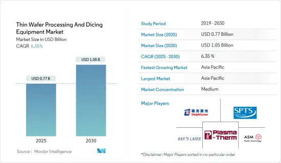
薄ウエハー加工・ダイシング装置市場規模は、2025年に7億7,000万米ドルと推定され、予測期間(2025年~2030年)のCAGRは6.35%で、2030年には10億5,000万米ドルに達すると予測されています。
主なハイライト
- 電子部品の使用量増加による莫大な需要により、電子パッケージングを高度に資源化する取り組みが増加しており、電子パッケージングは無数の用途で有用となっています。こうした要因が半導体・ICパッケージ市場の成長を後押ししています。
- 今後数年間で、薄型ウエハー加工およびダイシング装置の需要を押し上げると予想される主な要因の1つは、メモリーカード、スマートフォン、スマートカード、各種コンピューティングデバイスなどの小型半導体デバイスに広く使用されている3次元集積回路に対する需要の高まりです。
- 3次元回路は、高速性、耐久性、低消費電力、メモリの軽量化など、製品全体の性能を向上させるため、携帯家電、センサー、MEMS、工業製品など、スペースに制約のある複数のアプリケーションで普及が進んでいます。
- 低コストのクラウド・コンピューティング・ソリューションが普及しているため、さまざまな企業や産業でサーバーやデータセンター・システムの利用が拡大しており、マイクロプロセッサーやデジタル・シグナル・プロセッサーのようなロジック・デバイスの需要が高まる可能性が高いです。また、IoT対応リンク・デバイスの増加に伴い、マイクロプロセッサの利用も増加しています。これらのデバイスでは、効果的な温度管理を可能にし、性能を向上させるため、薄型ウエハーの採用が増えています。こうした要因が市場成長の要因となっています。
- シリコンウエハーは、マイクロエレクトロニクスやMEMSの製造プラットフォームとして長年使用されてきました。シリコン・オン・インシュレーター基板は、標準的なシリコン・ウエハーのユニークなバリエーションです。厚さ約1~2μmの二酸化シリコンのボンド層を使って2枚のウエハーを接着し、ウエハーを作る。1枚のウエハーは厚さ10~50μmに平坦化されます。コーティングの正確な厚さは用途によって決まる。
- 最新鋭の薄型ウエハー鋳造工場の建設コストは指数関数的に上昇し、市場を圧迫しています。半導体メーカーの数はこのところ統合されています。性能の向上は鈍化しており、特殊な薄型ウエハーの魅力はますます高まっています。薄型ウエハーが普遍的であることを可能にする設計上の決定は、一部のコンピューティング・タスクにとっては最適ではない可能性があります。
- 半導体研究におけるさまざまな開発が、市場にさらなるチャンスをもたらしています。例えば、2023年4月、ラピダスは正式にImecのコアパートナープログラムに参加し、先端半導体研究におけるImecとの持続可能な協力関係を大きく前進させました。この動きは、半導体領域における長期的なコラボレーションと進歩へのコミットメントを強化するものです。
薄ウエハー加工・ダイシング装置市場動向
半導体の小型化ニーズの高まりが市場を牽引
- 米国消費者技術協会(Consumer Technology Association)によると、米国では2022年から2024年にかけて家電製品の小売売上高が微増し、その総額は5,000億米ドルを超えると予想されています。これにより、電子製品を開発するためのウエハー需要が増加すると思われます。ヘルスケアや車載用半導体ICメーカーなど他のエンドユーザーとともに、家電製品の需要はICの小型化を余儀なくされています。そのため、市場の小型化が進み、予測期間中に需要が急増すると予想されます。
- 地域別では、ファブレス・ビジネスモデルが、世界の半導体販売においてアジア諸国が突出した地位を占める主な要因となっています。ファブレス企業は通常、純粋な鋳造所やアウトソーシング組立・テスト(OSAT)企業に製造を委託しています。
- 富士フイルムによると、AI、IoT、次世代通信規格「5G」の利用拡大や自律走行技術の進展により、半導体の需要や性能の向上が見込まれるため、半導体デバイスの微細化が続いています。上記のような要因から、最高の性能を発揮するために、極薄シリコンウエハー上に構築された3次元回路アーキテクチャに依存する小型・軽量の消費者向けデバイスの需要が高まっています。
- このウエハーは極めて薄く平坦です。同時に、小型化により、1つのチップに複数の機能を集積する必要が生じています。直径12インチの大型ウエハーにより、ウエハー技術に新たな動向が見られます。
- 2023年12月、サムスン電子とASMLホールディングNVは、韓国に先進的な研究開発(R&D)施設を設立するため、7億6,000万米ドルを共同で投資すると発表しました。この施設の主な目的は、半導体製造プロセスを強化することであり、特にASMLの最先端EUV技術の活用に重点を置いています。この戦略的パートナーシップは、前年に3μmチップの量産に成功したサムスンが、2025年までに2ナノメートルチップの商業化を目指す上で極めて重要です。
アジア太平洋が最大の市場シェアを占める見通し
- アジア太平洋は世界最大かつ最も急成長している半導体市場です。中国、韓国、シンガポールのような国々からのスマートフォンやその他のコンシューマーエレクトロニクスデバイスに対する大きな需要が、多くのベンダーに地域生産施設の設立を促しています。
- 中国のさまざまな市場企業は、買収や合併を通じて事業を拡大することに注力しています。例えば、2023年12月、中国の半導体設計企業はマレーシアのチップパッケージング企業と提携し、ハイエンドのグラフィックス・プロセッシング・ユニット(GPU)を組み立てた。中国のHuatian Technologyが大半を所有するUnisemや他のマレーシアのチップパッケージング企業は、中国のパートナーからのビジネスや問い合わせの増加に気づいた。中国のXfusionやStarFiveのような企業は、マレーシアでの事業拡大を計画していました。
- 世界の半導体産業における力学の変化を考えると、ベトナムやインドのような他の国もチップ製造サービスの代替になろうとしています。このシフトは、中国企業が中国国外でチップを組み立てることを選択し、地政学的リスクを軽減し、国外市場への参入を容易にしていることを示しています。
- 日本は、複数の大手メーカーとエレクトロニクス産業の本拠地であるため、半導体産業において不可欠な地位を占めています。政府は、大手チップメーカーの国内進出の可能性を調査する見込みです。一方、日本の組織は、半導体製造とパッケージングで消費される最も重要な材料の重要なサプライヤーと見なされています。日本のサプライヤーにとって、日本の為替レートと高い製造コストは、材料をより高価なものにし、ローエンド・アプリケーション向けの他のサプライヤーにチャンスを開いています。
- オーストラリアでは電子機器製造業が成長しており、様々なエンドユーザー産業で先端機器の採用が増加していることが市場成長に影響を与えています。主にテレビやスマートフォンの販売が家電製品の増加を牽引しています。
- 2023年12月、シドニー大学ナノ研究所は、レゴブロックのように設計され、帯域幅が改善された新しいチップを発表しました。このコンパクトなシリコン半導体チップは、エレクトロニクスとフォトニック・コンポーネントをスムーズに組み合わせたものです。この画期的な技術により、無線周波数(RF)の帯域幅が大幅に広がり、チップ内の情報管理の精度が向上します。先進的なシリコンフォトニクス技術を活用したこのチップは、5ミリメートル以下の幅にさまざまな半導体システムを統合する能力を備えています。
- 完全自動運転車の成長軌道は、技術の進歩、完全自動運転車を受け入れる消費者の意欲、価格設定、自動車の安全性に関する重大な懸念に対処するサプライヤーやOEMの能力など、アジア太平洋の要因に大きく影響されます。これらの要因から、自動車業界と半導体業界は常に技術の強化、原材料価格の交渉、自動車と信頼できる技術の組み合わせに集中しています。
薄ウエハー加工・ダイシング装置産業概要
薄ウエハー加工・ダイシング装置市場は半固体化しており、ディスコ、パナソニック、日本、台湾パルスモーターなど、ごく少数の大手企業で構成されています。同市場は、薄ウェーハの製造プロセスにおいて依然として大きな課題に直面しています。上記の要因により、新規参入の動きは鈍いです。とはいえ、市場各社の絶え間ない技術革新と研究開発努力は、競争力の維持に役立っています。そのため、市場における競争企業間の敵対関係は緩やかです。
- 2024年3月:日立ハイテクは、ノンパターンウエハーの表裏面のパーティクルや欠陥を検査する新システム「LS9300AD」の発売を発表しました。LS9300ADは、従来の暗視野レーザー散乱法による異物・欠陥検出に加え、新たにDIC(微分干渉コントラスト)検査機能を搭載し、浅い低アスペクトの微細な凹凸欠陥も検出することができます。LS9300ADは、従来製品で採用しているウエハーエッジグリップ方式と回転ステージを採用し、ウエハーの表裏検査が可能です。
- 2023年11月コーニングは、ドイツのレーザー技術事業を中国のSuzhou Delphi Laserに売却しました。この契約は、コーニング・レーザー・テクノロジーズとして知られる部門の全株式を蘇州デルファイ・レーザー社が取得するものでした。
その他の特典:
- エクセル形式の市場予測(ME)シート
- 3ヶ月間のアナリストサポート
目次
第1章 イントロダクション
- 調査の前提条件と市場定義
- 調査範囲
第2章 調査手法
第3章 エグゼクティブサマリー
第4章 市場洞察
- 市場概要
- 業界の魅力度ポーターのファイブフォース分析
- 新規参入業者の脅威
- 買い手の交渉力
- 供給企業の交渉力
- 代替品の脅威
- 競争企業間の敵対関係の強さ
- 業界バリューチェーン分析
- COVID-19の副作用とその他のマクロ経済要因が市場に与える影響
第5章 市場力学
- 市場促進要因
- スマートカード、RFID技術、車載用パワーICの需要増加
- 半導体の小型化ニーズの高まり
- 市場抑制要因
- 製造上の課題
第6章 市場セグメンテーション
- 装置タイプ別
- 薄膜化装置
- ダイシング装置
- ブレードダイシング
- レーザーアブレーション
- ステルスダイシング
- プラズマダイシング
- 用途別
- メモリ・ロジック(TSV)
- MEMSデバイス
- パワーデバイス
- CMOSイメージセンサー
- RFID
- その他
- ウエハー厚さ別
- 750マイクロメートル
- 120マイクロメートル
- 50マイクロメートル
- ウエハーサイズ別
- 4インチ以下
- 5インチおよび6インチ
- 8インチ
- 12インチ
- 地域別
- 北米
- 欧州
- アジア
- オーストラリア・ニュージーランド
- ラテンアメリカ
- 中東・アフリカ
第7章 競合情勢
- 企業プロファイル
- Suzhou Delphi Laser Co. Ltd
- SPTS Technologies Limited
- Plasma-Therm LLC
- Han's Laser Technology Industry Group Co. Ltd
- ASM Laser Separation International(ALSI)BV
- Disco Corporation
- Tokyo Seimitsu Co, Ltd(Accretech)
- Neon Tech Co. Ltd
- Advanced Dicing Technologies Ltd
- Panasonic Corporation
- Hitachi High-Tech Corporation
第8章 投資分析
第9章 市場機会と今後の動向
The Thin Wafer Processing And Dicing Equipment Market size is estimated at USD 0.77 billion in 2025, and is expected to reach USD 1.05 billion by 2030, at a CAGR of 6.35% during the forecast period (2025-2030).
Key Highlights
- The increasing efforts to make electronic packaging highly resourceful due to the enormous demand for electronic components owing to amplified usage have made electronic packaging useful in a myriad of applications. These factors are driving the growth of the semiconductor and IC packaging market.
- One of the major factors expected to boost the demand for thin wafer processing and dicing equipment in the coming years is the growing demand for three-dimensional integrated circuits, which are widely used in miniature semiconductor devices such as memory cards, smartphones, smart cards, and various computing devices.
- Three-dimensional circuits are becoming more popular in multiple space-constrained applications, such as portable consumer electronics, sensors, MEMS, and industrial products because they improve overall product performance in terms of speed, durability, low power consumption, and lightweight memory.
- Due to the widespread availability of low-cost cloud computing solutions, the expanding use of server and data center systems across various enterprises and industries is likely to fuel demand for logic devices like microprocessors and digital signal processors. In addition, as the number of IoT-enabled linked devices grows, the utilization of microprocessors also increases. Thin wafers are increasingly employed in these devices to enable effective temperature management and enhance performance. Such factors are responsible for the growth of the market.
- Silicon wafers have long been used as a fabrication platform in microelectronics and MEMS. The silicon-on-insulator substrate is a unique variation of the standard silicon wafer. Two silicon wafers are glued together using a bond layer of silicon dioxide with a thickness of about 1-2 μm to make these wafers. One silicon wafer gets flattened down to 10-50 μm in thickness. The application will determine the exact thickness of the coating.
- The cost of building state-of-the-art thin wafer foundries has increased exponentially, which puts pressure on the market. The number of semiconductor manufacturers has consolidated in recent times. Performance boosts are slowing down, making specialized thin wafers increasingly attractive. The design decisions that enable thin wafers to be universal may be sub-optimal for some computing tasks.
- Various developments in semiconductor research further create opportunities for the market. For instance, in April 2023, Rapidus officially joined Imec's Core Partner Program, marking a significant stride in sustainable collaboration with Imec in advanced semiconductor research. This move reinforced their commitment to long-term collaboration and advancement in the semiconductor domain.
Thin Wafer Processing And Dicing Equipment Market Trends
Increasing Need for Miniaturization of Semiconductors is Expected to Drive the Market
- According to the Consumer Technology Association, in the US, retail sales of consumer electronics were expected to grow marginally between 2022 and 2024, with the total value exceeding USD 500 billion. This would increase the demand for wafers to develop electronic products. The demand for consumer electronics products, along with other end users such as healthcare and automotive semiconductor IC manufacturers, is forcing them to reduce the size of ICs. It has, therefore, given rise to miniaturization in the market, which is expected to experience a surge in its demand during the forecast period.
- Across geographies, the fabless business model is the major contributor to the prominent position of various Asian countries in semiconductor sales worldwide. Fabless firms typically outsource fabrication to pure-play foundries and outsourced assembly and test (OSAT) firms.
- According to Fujifilm, the miniaturization of semiconductor devices continues as the increasing use of AI, IoT, and next-generation communication standard '5G' and the advancement of autonomous driving technology are expected to increase the demand for and performance of semiconductors. The factors mentioned above have led to the rise in demand for small and lightweight consumer devices that rely on 3D circuit architecture built onto ultra-thin silicon wafers in order to perform at peak capacity.
- These wafers are extremely thin and flat. At the same time, miniaturization has resulted in the need to integrate several features on a single chip. Due to large-sized wafers (with a diameter of up to 12 inches), there is a new trend in wafer technology.
- In December 2023, Samsung Electronics and ASML Holding NV announced a collaborative investment of USD 760 million to establish an advanced Research and Development (R&D) facility in South Korea. The primary objective of this facility is to enhance semiconductor manufacturing processes, with a specific focus on utilizing ASML's cutting-edge EUV technology. This strategic partnership is crucial for Samsung's goal of commercializing 2-nanometer chips by 2025, building on the successful mass production of 3 µm chips in the preceding year.
Asia-Pacific is Expected to Hold the Largest Market Share
- The Asia-Pacific is the largest and fastest-growing semiconductor market in the world. Significant demand for smartphones and other consumer electronics devices from countries such as China, the Republic of Korea, and Singapore encourages many vendors to set up regional production establishments.
- China's various market players are focusing on expanding business through acquisitions and mergers. For instance, in December 2023, Chinese semiconductor design companies teamed up with Malaysian chip packaging firms to assemble high-end graphics processing units (GPUs). Unisem, the majority of which is owned by China's Huatian Technology, and other Malaysian chip packaging companies noticed an uptick in business and inquiries from their Chinese partners. Companies like Xfusion and StarFive from China planned to expand their operations in Malaysia.
- Given the changing dynamics in the global semiconductor industry, other countries like Vietnam and India are also trying to become alternatives for chip manufacturing services. This shift shows that Chinese companies are choosing to assemble their chips outside China, reducing geopolitical risks and making it easier to reach markets outside the country.
- Japan occupies an essential position in the semiconductor industry as it is home to several major manufacturers and the electronics industry. The government is expected to investigate the potential for bringing major chip makers into the country. Meanwhile, Japanese organizations are considered significant suppliers of the most critical materials consumed in semiconductor manufacturing and packaging. For Japanese suppliers, Japanese exchange rates and high production costs make materials more expensive and open up opportunities for other suppliers for low-end applications.
- The growing electronics manufacturing sector in Australia and the increasing adoption of advanced devices among various end-user industries influence market growth. The sales of televisions and smartphones have primarily driven the increase in consumer electronics.
- In December 2023, the University of Sydney Nano Institute unveiled a new chip designed like LEGO blocks, featuring improved bandwidth. This compact silicon semiconductor chip smoothly combines electronics with photonic components. The breakthrough will significantly increase radio-frequency (RF) bandwidth and enhance the precision of managing information within the chip. Utilizing advanced silicon photonics technology, the chip has integration capabilities for various semiconductor systems, all within a width of less than 5 millimeters.
- The growth trajectory of fully autonomous automobiles is heavily influenced by factors in Asia-Pacific, including technology advancements, consumer willingness to accept fully automated vehicles, pricing, and suppliers' and OEMs' capacity to address significant concerns about vehicle safety. According to these factors, the automotive and semiconductor industries always concentrate on enhancing technologies, negotiating raw material prices, and combining cars with reliable technology.
Thin Wafer Processing And Dicing Equipment Industry Overview
The market for thin wafer processing and dicing is semi-consolidated and comprises very few major players, such as Disco Corporation, Panasonic Corporation, Nippon, and Pulse Motor Taiwan. The market still faces considerable challenges in the manufacturing processes of thin wafers. The above-mentioned factor has led to a slower entry of new players into the market. Nevertheless, the constant innovations and R&D efforts of market players help maintain a competitive edge. Therefore, competitive rivalry in the market is moderate.
- March 2024: Hitachi High-Tech Corporation announced the launch of the LS9300AD, a new system for inspecting the front and back sides of non-patterned wafer surfaces for particles and defects. In addition to the conventional dark-field laser scattering detection of foreign material and defects, the LS9300AD is equipped with a new DIC (Differential Interference Contrast) inspection function that enables the detection of irregular defects, even shallow, low-aspect microscopic defects. LS9300AD has the wafer edge grip method and rotating stage used in conventional products to enable front and backside wafer inspection.
- November 2023: Corning Inc. sold its German laser technology business to Suzhou Delphi Laser in China. The agreement involved Suzhou Delphi Laser acquiring the complete stake in the division known as Corning Laser Technologies.
Additional Benefits:
- The market estimate (ME) sheet in Excel format
- 3 months of analyst support
TABLE OF CONTENTS
1 INTRODUCTION
- 1.1 Study Assumptions and Market Definition
- 1.2 Scope of the Study
2 RESEARCH METHODOLOGY
3 EXECUTIVE SUMMARY
4 MARKET INSIGHTS
- 4.1 Market Overview
- 4.2 Industry Attractiveness Porter's Five Forces Analysis
- 4.2.1 Threat of New Entrants
- 4.2.2 Bargaining Power of Buyers
- 4.2.3 Bargaining Power of Suppliers
- 4.2.4 Threat of Substitute Products
- 4.2.5 Intensity of Competitive Rivalry
- 4.3 Industry Value Chain Analysis
- 4.4 Impact of COVID-19 Aftereffects and Other Macroeconomic Factors on the Market
5 MARKET DYNAMICS
- 5.1 Market Drivers
- 5.1.1 Increasing Demand for Smart Cards, RFID Technology, and Automotive Power ICs
- 5.1.2 Increasing Need for Miniaturization of Semiconductors
- 5.2 Market Restraint
- 5.2.1 Manufacturing Challenges
6 MARKET SEGMENTATION
- 6.1 By Equipment Type
- 6.1.1 Thinning Equipment
- 6.1.2 Dicing Equipment
- 6.1.2.1 Blade Dicing
- 6.1.2.2 Laser Ablation
- 6.1.2.3 Stealth Dicing
- 6.1.2.4 Plasma Dicing
- 6.2 By Application
- 6.2.1 Memory and Logic (TSV)
- 6.2.2 MEMS Devices
- 6.2.3 Power Devices
- 6.2.4 CMOS Image Sensors
- 6.2.5 RFID
- 6.2.6 Others
- 6.3 By Wafer Thickness
- 6.3.1 750 micrometers
- 6.3.2 120 micrometers
- 6.3.3 50 micrometers
- 6.4 By Wafer Size
- 6.4.1 Less than 4 inches
- 6.4.2 5 inches and 6 inches
- 6.4.3 8 inches
- 6.4.4 12 inches
- 6.5 By Geography
- 6.5.1 North America
- 6.5.2 Europe
- 6.5.3 Asia
- 6.5.4 Australia and New Zealand
- 6.5.5 Latin America
- 6.5.6 Middle East and Africa
7 COMPETITIVE LANDSCAPE
- 7.1 Company Profiles
- 7.1.1 Suzhou Delphi Laser Co. Ltd
- 7.1.2 SPTS Technologies Limited
- 7.1.3 Plasma-Therm LLC
- 7.1.4 Han's Laser Technology Industry Group Co. Ltd
- 7.1.5 ASM Laser Separation International (ALSI) BV
- 7.1.6 Disco Corporation
- 7.1.7 Tokyo Seimitsu Co, Ltd (Accretech)
- 7.1.8 Neon Tech Co. Ltd
- 7.1.9 Advanced Dicing Technologies Ltd
- 7.1.10 Panasonic Corporation
- 7.1.11 Hitachi High-Tech Corporation

