
|
市場調査レポート
商品コード
1928874
薄型ウエハー加工およびダイシング装置の市場機会、成長要因、業界動向分析、ならびに2026年から2035年までの予測Thin Wafer Processing and Dicing Equipment Market Opportunity, Growth Drivers, Industry Trend Analysis, and Forecast 2026 - 2035 |
||||||
カスタマイズ可能
|
|||||||
| 薄型ウエハー加工およびダイシング装置の市場機会、成長要因、業界動向分析、ならびに2026年から2035年までの予測 |
|
出版日: 2026年01月06日
発行: Global Market Insights Inc.
ページ情報: 英文 180 Pages
納期: 2~3営業日
|

概要
世界の薄型ウエハー加工・ダイシング装置市場は、2025年に8億4,480万米ドルと評価され、2035年までにCAGR7.3%で成長し、17億米ドルに達すると予測されています。
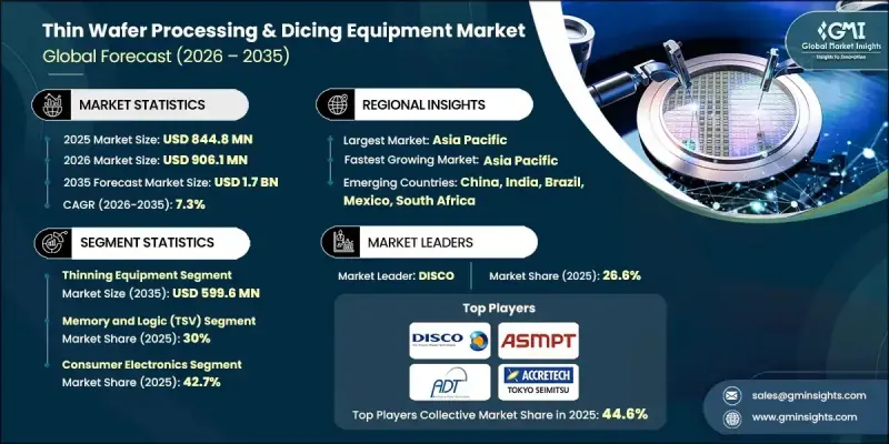
市場成長は、半導体デバイスの複雑化とバックエンド製造における高精度化の必要性によって支えられています。より薄く、より軽く、より信頼性の高い部品への需要増加は、バリューチェーン全体における装置要件の変革を継続的に進めています。デバイス構造と材料の進歩により、精度、歩留まり向上、材料応力低減がより重視されるようになりました。装置サプライヤーは、構造的完全性を維持しながら精密なウエハー薄化と分離を可能にする先進的なソリューションを提供することで対応しています。次世代パッケージング手法の採用は、高精度プロセスへの需要をさらに高めています。製造業者は、大規模な半導体生産を支えるため、生産性、コスト効率、プロセス安定性を優先します。自動化とインテリジェントシステムは、スループットの向上、ダウンタイムの削減、品質管理の強化において、ますます重要な役割を果たしています。これらの要因が相まって、薄型ウエハー加工およびダイシング装置は、世界の半導体産業における革新とスケーラビリティの重要な推進力として確立されています。
| 市場範囲 | |
|---|---|
| 開始年 | 2025年 |
| 予測年度 | 2026-2035 |
| 開始時価値 | 8億4,480万米ドル |
| 予測金額 | 17億米ドル |
| CAGR | 7.3% |
装置サプライヤーは、歩留まりの向上と脆弱化するウエハー構造のサポートを目的に、非接触・低ストレス加工技術の進化を続けております。寸法精度、表面品質、運用効率への注目の高まりは、デバイス高密度化という業界全体の動向を反映しております。自動化およびデータ駆動型システムは、製造ライン全体におけるプロセス制御の改善、欠陥削減、予知保全を支えております。
薄膜化装置セグメントは、2035年までに5億9,960万米ドルに達すると予測されています。半導体メーカーがコンパクトで高性能なデバイスを支える超薄型ウエハーへの移行を進めるにつれ、需要は増加しています。精密加工技術の継続的な改善は、歩留まりの向上、応力レベルの低減、および先進デバイス製造で使用される繊細なウエハーとの互換性向上に貢献しています。
MEMSデバイス分野は、2026年から2035年にかけてCAGR8.6%で成長すると予測されています。コンパクトで信頼性が高く、高精度の部品を必要とする複数の最終用途産業における採用拡大が成長を牽引しています。超薄型ウエハーの取り扱いと先進的な分離技術の活用増加により、一貫性と信頼性が向上しています。自動化とリアルタイム監視システムは、歩留まり最適化をさらに支援します。
欧州の薄型ウエハー加工・ダイシング装置市場は、2025年に1億6,140万米ドル規模に達し、予測期間を通じて堅調な成長が見込まれます。地域需要は、特に複数産業における高性能・高精度アプリケーション向けの先進半導体製造への継続的な投資によって支えられています。
よくあるご質問
目次
第1章 調査手法と範囲
第2章 エグゼクティブサマリー
第3章 業界考察
- エコシステム分析
- サプライヤーの情勢
- 利益率分析
- コスト構造
- 各段階における付加価値
- バリューチェーンに影響を与える要因
- ディスラプション
- 業界への影響要因
- 促進要因
- 小型化された電子デバイスへの需要の高まり
- 5Gおよび高性能コンピューティングアプリケーションの普及
- 先進半導体材料の利用拡大
- 自動車用電子機器および電気自動車(EV)の成長
- 業界の潜在的リスク&課題
- 高度なダイシング装置の高コスト
- 薄型化されたウエハーの脆弱性の増加
- 市場機会
- 人工知能と自動化技術によるウエハーハンドリングの統合
- MEMS、光、RFデバイス製造の成長
- 促進要因
- 成長可能性分析
- 規制情勢
- 北米
- 欧州
- アジア太平洋地域
- ラテンアメリカ
- 中東・アフリカ
- ポーターの分析
- PESTEL分析
- 技術とイノベーションの動向
- 現在の技術動向
- 新興技術
- 新興ビジネスモデル
- コンプライアンス要件
- 特許および知的財産分析
- 地政学的・貿易動向
第4章 競合情勢
- イントロダクション
- 企業の市場シェア分析
- 地域別
- 北米
- 欧州
- アジア太平洋地域
- ラテンアメリカ
- 中東・アフリカ
- 地域別
- 主要企業の競合ベンチマーキング
- 財務実績比較
- 収益
- 利益率
- 研究開発
- 製品ポートフォリオ比較
- 製品ラインの広さ
- 技術
- イノベーション
- 地域別展開比較
- 世界展開分析
- サービスネットワークのカバー率
- 地域別市場浸透率
- 競合ポジショニングマトリックス
- リーダー企業
- 課題者
- フォロワー
- ニッチプレイヤー
- 戦略的展望マトリックス
- 財務実績比較
- 主な発展, 2021-2024
- 合併・買収
- 提携および共同事業
- 技術的進歩
- 拡大と投資戦略
- デジタルトランスフォーメーションの取り組み
- 新興/スタートアップ競合の動向
第5章 市場推計・予測:装置タイプ別、2022-2035
- 薄膜化装置
- ダイシング装置
- ブレードダイシング
- レーザーダイシング
- ステルスダイシング
- プラズマダイシング
- ハンドリング・サポート装置
- 仮接合/剥離システム
- ウエハー実装/剥離システム
- 洗浄・検査システム
第6章 市場推計・予測ウエハーサイズ別、2022-2035
- 4インチ未満
- 5インチおよび6インチ
- 8インチ
- 12インチ
第7章 市場推計・予測:ウエハー厚さ別、2022-2035
- 750µm(標準/比較的厚い)
- 120µm(先進的な主流)
- 50µm以下
第8章 市場推計・予測:用途別、2022-2035
- CMOSイメージセンサー
- メモリおよびロジック(TSV)
- MEMSデバイス
- パワーデバイス
- RFID
- その他
第9章 市場推計・予測:最終用途産業別、2022-2035
- 民生用電子機器
- 自動車
- 電気通信
- ヘルスケア
- 航空宇宙・防衛
- 産業用
- その他
第10章 市場推計・予測:地域別、2022-2035
- 北米
- 米国
- カナダ
- 欧州
- ドイツ
- 英国
- フランス
- スペイン
- イタリア
- オランダ
- アジア太平洋地域
- 中国
- インド
- 日本
- オーストラリア
- 韓国
- ラテンアメリカ
- ブラジル
- メキシコ
- アルゼンチン
- 中東・アフリカ
- 南アフリカ
- サウジアラビア
- アラブ首長国連邦
第11章 企業プロファイル
- 世界の主要企業
- DISCO Corporation
- ASMPT
- KLA Corporation
- Lam Research Corporation
- 地域別主要企業
- 北米
- Plasma-Therm
- SPTS Technologies Ltd.
- Loadpoint Ltd.
- 欧州
- Synova SA
- Modutek Corporation
- Dynatex International
- アジア太平洋
- Tokyo Electron Limited
- TOKYO SEIMITSU CO., LTD(Accretech)
- Panasonic Connect Co., Ltd.
- 北米
- ニッチプレイヤー/ディスラプター
- Advanced Dicing Technologies
- AXUS TECHNOLOGY
- Citizen Chiba Precision Co., Ltd.
- HANMI Semiconductor
- Han's Laser Technology Co., Ltd.
- NeonTech Co.,Ltd.
- Suzhou Delphi Laser Co., Ltd.

