
半導体ボンディング装置:市場シェア分析、業界動向と統計、成長予測(2026年~2031年)
Semiconductor Bonding Equipment - Market Share Analysis, Industry Trends & Statistics, Growth Forecasts (2026 - 2031)- 発行日
- ページ情報
- 英文 120 Pages
- 納期
- 2~3営業日
- 商品コード
- 2035144
- カスタマイズ可能 お客様のご希望に応じて、既存データの加工や未掲載情報(例:国別セグメント)の追加などの対応が可能です。詳細はお問い合わせください。
- 適宜更新あり 本レポートは最新情報反映のため適宜更新し、内容構成変更を行う場合があります。ご検討の際はお問い合わせください。
- 翻訳ツール提供対象 PDF対応AI翻訳ツールの無料貸し出しサービスのご利用が可能です
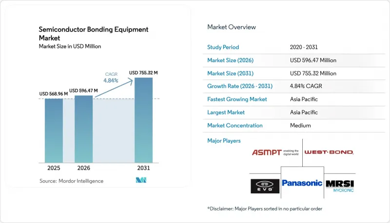
2026年の半導体ボンディング装置の市場規模は5億9,647万米ドルと推定されており、2025年の5億6,896万米ドルから拡大し、2031年には7億5,532万米ドルに達すると予測されています。
2026年から2031年にかけては、CAGR 4.84%で成長すると見込まれています。
需要の伸びは、業界が平面微細化から垂直積層へと移行していることを反映しており、この分野では、異種集積戦略により、ウエハー間およびダイとウエハー間の精密な接続が求められています。主要なチップメーカーは、AIアクセラレータや高性能コンピューティングデバイスの帯域幅、レイテンシ、エネルギー効率を向上させるため、先進的なパッケージングラインへの設備投資を加速させています。3nm以下のノードがリスク生産段階に移行するにつれ、ハイブリッド銅ー銅プロセスが従来のワイヤボンディングに取って代わりつつあり、アライメント精度に対する要求は10µm未満へと高まっています。同時に、自動車の電動化やIoTの小型化により、アプリケーションの適用範囲が広がり、恒久型、一時型、およびハイブリッド型プラットフォームの受注残高が増加しています。しかし、総所有コストの高さや揮発性有機化合物(VOC)に関する環境規制の強化により、稼働率を70%以上に維持するというプレッシャーが高まっており、購入者はフルサービス契約や予知保全パッケージの交渉を進めています。
世界の半導体ボンディング装置市場の動向と洞察
IDMおよびファウンダリによる設備投資(CAPEX)の増加
世界の半導体製造装置への投資額は2024年に1,100億米ドルに達し、2026年までに1,300億米ドルに達する見込みです。TSMCだけでも、2025年の設備更新に380億~420億米ドルを計上しており、その大部分は先進的なパッケージングおよびボンディングラインへの資金充てられています。サムスンやインテルによる同様の拡張は、高帯域幅メモリやチプレット設計を支えるウエハーレベル集積化に対する競合上の必要性を強調しています。現在、資本配分の対象となっているのは、サブミクロン級の光学アライメントモジュール、真空ボンディングチャンバー、AIを活用したプロセス制御などの項目です。デバイスメーカーが将来の設計変更に備える中、モジュール式のアップグレードパスを提供するベンダーが優先サプライヤーとしての地位を確立しつつあります。この投資の増加は、交換サイクルの短縮や、フロントエンドおよびバックエンドのファブ双方における導入基盤の拡大を通じて、半導体ボンディング装置市場を活性化させています。
自動車およびIoTデバイスにおける半導体搭載量の急増
電動パワートレイン、先進運転支援システム(ADAS)、ゾーンアーキテクチャの普及により、2024年には1台あたりの平均半導体搭載額は950米ドルに達しました。電気自動車モデルでは、高力・高温対応のボンディングヘッドと堅牢なフラックス管理システムを必要とする炭化ケイ素(SiC)および窒化ガリウム(GaN)パワーデバイスが採用されています。並行して、IoTウェアラブル機器やスマートホームノードでは、フットプリントを縮小し、バッテリー寿命を延長するウエハーレベルチップスケールパッケージが求められています。これらの異なる要件は装置レベルで収束しており、構成可能なボンダーは、高出力の圧力プロファイルと繊細なMEMSの取り扱いとの間で切り替えを行う必要があります。サプライヤー各社は、適応型クランプ設計、チャックの平面度に関するリアルタイムフィードバック、およびレシピ駆動型の圧力曲線により、このギャップへの対応を進めています。この動向により、半導体ボンディング装置市場における出荷台数が増加する一方で、自動車ティア1サプライヤーや民生用OEMメーカーにまたがる収益源の多様化が進んでいます。
高い所有コストとTCOの不確実性
最先端のハイブリッドボンダーの価格は300万米ドルを超えますが、スペアパーツ、消耗品、校正を含む年間ランニングコストにより、ライフタイムコストは800万米ドルに達する可能性があります。小規模なOSAT(受託半導体組立業者)は、稼働率が70%を下回ると苦戦を強いられます。特に、民生用電子機器の閑散期にはその傾向が顕著です。ロードマップの急速な更新は財務モデリングをさらに複雑にしています。なぜなら、10µmのオーバーレイに対応したツールであっても、わずか2回の製品サイクル後に改造キットが必要になる可能性があるからです。リースプログラム、成果連動型サービス契約、リスク分担型価格モデルが登場しつつありますが、CFO(最高財務責任者)らは依然として、残存価値の不確実性を、半導体ボンディング装置市場における新規発注の足かせとして挙げています。
セグメント分析
CAGR5.88%で最も急速な成長を記録しており、ウエハーの薄型化やTSV(貫通電極)の形成に対応し、機械的サポートに必要な可逆的な接着を提供します。ハイブリッドシステムはCAGR5.88%で最も急速な成長を記録しており、銅対銅のダイレクトアタッチにより抵抗とエレクトロマイグレーションを最小限に抑える3nm以下の集積化をターゲットとしています。この成長により、ハイブリッドプラットフォーム向けの半導体ボンディング装置市場規模は、控えめなベースから、この10年が終わる前に恒久型装置と同等の水準へと拡大する見込みです。メーカー各社は、2段階アライメント光学系、アクティブレベリングチャック、クローズドループ圧力制御といった技術で差別化を図っており、これらを組み合わせることで配置誤差を500 nm未満に抑えています。購入者は、将来のレシピ追加に対応可能なマルチモードユニットを好んでおり、これにより資本リスクを低減しています。この転換に伴い、剥離することなく繰り返しの熱サイクルに耐えるヒートスプレッダー材料や、コンプライアントなアンダーフィル化学組成に関する研究開発が活発化しています。競合はスループットにもかかっており、現在、主力機種では、並列クランプアームと予測サーボチューニングにより、サイクルタイムを20%短縮することを約束しています。
この変化に伴い、装置の更新サイクルも拡大しています。ライン管理者が旧式の共晶ボンダーを点検したところ、メンテナンス費用が年間12%増加していることが判明しました。ハイブリッドボンダーへの切り替えにより、2回工程が不要となり、フロア利用率が向上します。しかし、利害関係者は、ダイのシリアル番号レベルまでのトレーサビリティを管理するMESやファクトリーオートメーション層と、新しい装置がシームレスに統合されることを求めています。これに対し、ベンダーはOPC-UAゲートウェイやエッジ分析機能を組み込み、プロセスデータをAIベースの歩留まりダッシュボードに集約することで対応しています。このようなエコシステムとの互換性は、工場全体での導入を加速させ、半導体ボンディング装置市場におけるハイブリッドセグメントの貢献度を高めています。
アドバンスト・パッケージングは2025年の売上高の35.42%を占め、引き続き中核セグメントとしての地位を維持しており、チプレット・プロセッサ、高帯域幅メモリ、およびプレミアム・スマートフォンSoCプログラムによって支えられています。パワーICボンディングは、それほど注目度は高くありませんが、厳格なボイド制御プロトコルと高圧熱圧縮ヘッドに依存した安定した生産量を確保しています。シリコンフォトニクスは、CAGR5.73%という、際立った急成長ニッチ市場です。スイッチASICとコパッケージされた光学エンジンでは、シリコンキャリアウエハー上にゲルマニウム光検出器やIII-V族レーザーをミクロン単位の精度で配置する必要があり、250°C未満で温度上昇を制御した特殊なボンディングプロセスが求められています。この堅調な需要の推移により、シリコンフォトニクス分野のシェアは、半導体ボンディング装置市場全体において、すでに一桁台から二桁台へと拡大しています。
MEMSセンサー、特に自動車用LiDARや産業用オートメーション向けのものには、1,000サイクルの温度変動に耐える気密シールが求められます。このような応力プロファイルは、ガラスフリットボンディングや陽極ボンディングに適しており、ニッチな装置ベンダーの市場での地位を維持しています。CMOSイメージセンサーは、光軸の整合性を確保するためにアライメント精度を追求しており、ボンディングヘッドに組み込まれた高度なオートフォーカス光学系への受注を後押ししています。一方、RFデバイスは特有のインピーダンスをもたらし、低損失の配線メタリクスを必要とするため、次世代装置の材料供給サブシステムに影響を与えています。こうした広範な用途と新興用途の融合が、サプライヤーを景気変動から守り、半導体ボンディング装置市場を安定した成長軌道に乗せ続けています。
地域別分析
アジア太平洋地域は2025年の売上高の52.64%を占め、中国単独での装置投資額が前年比35%増の496億米ドルに達したことがその背景にあります。韓国が205億米ドルでこれに続き、台湾は一時的な在庫調整があったにもかかわらず、166億米ドルを貢献しました。各地域の政策パッケージには、税額控除、関税免除、インフラ補助金などが含まれており、これらがハイブリッドボンダーの実質的な購入価格を引き下げることで、半導体ボンディング装置市場における主導的地位を維持しています。TSMCやサムスンといった地元の有力企業が3Dおよびハイブリッド技術の採用を牽引しており、地域の技術水準を高めるとともに、精密チャックや超平坦キャリアウエハーに対するサプライチェーンの期待を再定義しています。
北米では2024年の売上高が137億米ドルを記録し、国内の生産能力拡大を目的としたCHIPS法の配分に伴い、14%の伸びを示しました。インテル、マイクロン、テキサス・インスツルメンツは、アリゾナ州、オハイオ州、テキサス州を拠点とする複数年にわたるパッケージングプロジェクトを発表しています。補助金による刺激策は受注を加速させていますが、助成金が段階的に縮小された後の長期的なコスト競争力に対する懸念も高まっています。しかし、同地域は、AIワークロード向けに低遅延インターポーザーを求めるハイパースケールデータセンターの顧客に近いという利点があり、この分野は半導体ボンディング装置市場において、より付加価値の高いハイブリッドボンダーの需要を創出しています。欧州では、アナログ、パワー、EUV装置ベンダーが集中するドイツとオランダに投資が集中しています。IPCEI-ME/CTのような共同プログラムは、特に厳格な信頼性が求められる自動車用パワーモジュール向けの3D集積化にEUの資金を投入しています。中東・アフリカ地域は依然として発展途上ですが、サウジアラビアの「ビジョン2030」やUAEの戦略的技術基金は、化合物半導体向けのパイロットラインに資金を割り当てています。こうした初期の動きは、従来のAPAC(アジア太平洋)の牙城を超えて、半導体ボンディング装置市場を段階的に拡大させる可能性のある、より広範な地域的多様化を示唆しています。
その他の特典:
- エクセル形式の市場予測(ME)シート
- 3ヶ月間のアナリストサポート
よくあるご質問
目次
第1章 イントロダクション
- 調査の前提条件と市場の定義
- 調査範囲
第2章 調査手法
第3章 エグゼクティブサマリー
第4章 市場情勢
- 市場概要
- 市場促進要因
- IDMおよびファウンダリによる設備投資の増加
- 自動車およびIoTデバイスにおける半導体搭載量の急増
- 先進的な2.5D/3Dパッケージングプラットフォームの急速な普及
- 政府主導の「CHIPS」補助金および税制優遇措置
- CISおよび3D-NANDにおけるハイブリッド・ウエハー間ボンディングの商用展開
- AIデータセンター向けシリコンフォトニック・インターポーザーがウエハーボンディング装置を牽引
- 市場抑制要因
- 高い所有コストとTCOの不確実性
- 10µm未満のアライメント公差におけるプロセスの複雑さ
- 超平坦ウエハーのサプライチェーンのボトルネック
- VOCおよび接着剤化学物質に関する環境規制の強化
- 業界バリューチェーン分析
- 規制情勢
- テクノロジーの展望
- ポーターのファイブフォース分析
- 供給企業の交渉力
- 買い手の交渉力
- 新規参入業者の脅威
- 代替品の脅威
- 競争企業間の敵対関係
- マクロ経済要因が市場に与える影響
第5章 市場規模と成長予測
- 機器別
- 恒久接合装置
- 一時ボンディング装置
- ハイブリッドボンディング装置
- 用途別
- 高度なパッケージング
- パワーICおよびディスクリート
- フォトニックデバイス
- MEMSセンサーおよびアクチュエータ
- エンジニアード・サブストレート
- RFデバイス
- CMOSイメージセンサー
- ボンディング技術別
- 熱圧縮ボンディング
- 共晶/はんだ接合
- 接着剤/ポリマーボンディング
- 超音波/サーモソニックボンディング
- 陽極接合/フュージョンボンディング
- ウエハーサイズ別
- 200 mm以下
- 200~300 mm
- 300 mm超
- エンドユーザー別
- 集積デバイスメーカー(IDM)
- ファウンダリ
- 半導体組立・試験受託業者(OSAT)
- 地域
- 北米
- 米国
- その他北米地域
- 南米
- 欧州
- ドイツ
- フランス
- その他欧州地域
- アジア太平洋地域
- 中国
- 日本
- 韓国
- インド
- その他アジア太平洋地域
- 中東
- アフリカ
- 北米
第6章 競合情勢
- 市場集中度
- 戦略的動向
- 市場シェア分析
- 企業プロファイル
- EV Group(EVG)
- ASMPT Semiconductor Solutions
- Mycronic AB(MRSI Systems)
- WestBond, Inc.
- Panasonic Holdings Corporation
- Palomar Technologies, Inc.
- Dr. Tresky AG
- BE Semiconductor Industries N.V.
- Fasford Technology Co., Ltd.
- Kulicke & Soffa Industries, Inc.
- DIAS Automation(HK)Ltd.
- Shibaura Mechatronics Corporation
- SUSS MicroTec SE
- Tokyo Electron Limited
- DISCO Corporation
- TOWA Corporation
- Hanmi Semiconductor Co., Ltd.
- Toray Engineering Co., Ltd.
- Hesse GmbH
- Finetech GmbH & Co. KG
第7章 市場機会と将来の展望
- 発行日
- 発行
- Mordor Intelligence
- ページ情報
- 英文 120 Pages
- 納期
- 2~3営業日


