|
|
市場調査レポート
商品コード
1687980
ファンアウトパッケージング:市場シェア分析、産業動向・統計、成長予測(2025年~2030年)Fan Out Packaging - Market Share Analysis, Industry Trends & Statistics, Growth Forecasts (2025 - 2030) |
||||||

|
|||||||
カスタマイズ可能
適宜更新あり
|
|||||||

| ファンアウトパッケージング:市場シェア分析、産業動向・統計、成長予測(2025年~2030年) |
|
出版日: 2025年03月18日
発行: Mordor Intelligence
ページ情報: 英文 125 Pages
納期: 2~3営業日
|

全表示
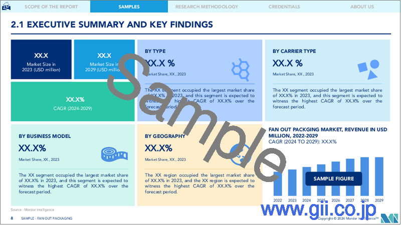
- 概要
- 目次
ファンアウトパッケージング市場規模は2025年に34億3,000万米ドルと推計され、2030年には73億5,000万米ドルに達すると予測され、市場推計・予測期間(2025-2030年)のCAGRは16.5%です。
この市場の拡大は、半導体をベースとした技術の進歩や、さまざまな分野での需要の急速な拡大が原動力となっています。
主なハイライト
- ファンアウトウエハーレベルパッケージング(FOWLP)は、高性能でエネルギー効率に優れた薄型・小型パッケージが求められるため、スマートフォンなど実装面積が重視されるデバイスへの応用が拡大しています。さらに、最近のスマートフォンには平均して5~7個のウエハーレベルパッケージ(特にファンアウト)が搭載されており、その数は今後も増加すると予想されています。これは、従来のパッケージ・オン・パッケージ(PoP)メモリ・オン・ロジック・ソリューションに徐々に取って代わりつつあるためです。
- さらに、さまざまな分野で人工知能や機械学習の応用が進んでいることから、市場での高性能コンピューティングの搭載が増加しています。UHDファンアウト技術は、クラウド、5G、自律走行車、AIチップへの応用が期待され、予測期間中のパッケージング動向をリードします。
- 韓国の半導体産業は、3D TSV(シリコン貫通電極)、パッケージング、FoWLP(ファンアウト・ウエハーレベル・パッケージング)、FoPLP(ファンアウト・パネルレベル・パッケージング)技術を改善し、半導体の性能と集積度を高めるために、より効果的にする努力を続けています。
- 2021年12月、ネペスラウエ社は、デカ社のMシリーズのファンアウト技術を用いた世界初の600mm×600mmの大型パネルレベルパッケージ(PLP)の生産に成功したと発表しました。同事業によると、ファンアウト・パネルレベル・パッケージング(FOPLP)ラインは第3四半期に顧客認証に合格し、安定した歩留まりを確立し、本格的な量産を開始しました。
- 韓国企業は従来、これらのシステムを海外企業に依存していたため、KOSTEKは今後大きな輸入代替効果を期待しています。一時的なウエハーボンダーとデボンディング技術は、ファンアウトパッケージング工程で使用できます。
- COVID-19の発生により、半導体パッケージング市場は、物品の移動が制限され、半導体のサプライチェーンに深刻な混乱が生じたため、成長が鈍化しました。2020年第1四半期、COVID-19は半導体ベンダーや流通チャネルの顧客に低在庫レベルをもたらしました。コロナウイルスの発生により、市場は長期的な影響を受けると予想されます。
ファンアウトパッケージング市場の動向
高密度ファンアウトが大きなシェアを占める
- ミッドレンジからハイエンドのアプリケーションをターゲットとする高密度ファンアウトは、1mm2あたり6~12個のI/Oを持ち、ライン/スペースは15/15μm~5/5μmです。高密度ファンアウトパッケージングは、携帯電話パッケージングのフォームファクターと性能要件に対応するために普及しました。この技術の主な構成要素は、再配分層(RDL)メタルとメガピラーめっきです。
- TSMCのInFO技術は、高密度ファンアウトの最も顕著な例の1つです。この技術は、アプリケーション・プロセッサ(AP)など、よりピン数の多いアプリケーションを対象としています。同社はFO-WLP分野をinFO-Antenna-in-Package(AiP)やinFO-on-Substrateなどの技術に拡大する計画です。これらのパッケージは自動車、サーバー、スマートフォンに使用されます。アップルはこの新技術をいち早く採用した企業のひとつで、2016年後半に発表されたiPhone 7のA10アプリケーション・プロセッサーに採用されました。
- このような利点から、2021年12月、クアルコムとメディアテックの両社は、iPhoneチップのパッケージにTSMCのInFO_PoP技術を利用するアップルの足跡をたどり、自社のフラッグシップ・スマートフォン・アプリケーション・プロセッサの製造にファンアウトPoPを採用することを検討しました。
- さらに、半導体市場の成長と高密度ファンアウト・パッケージング・ソリューションの開発が、予測期間中の市場成長を促進すると予想されます。例えば、2021年7月、世界有数の複合回路メーカーであり技術ソリューションプロバイダーであるChangdian Technology社は、XDFOIチップ用の超高密度ファンアウトパッケージングオプションの全ラインの正式導入を明らかにしました。これは、チップヘテロジニアス集積のためのコスト効率、高密度接続性、高集積、高信頼性ソリューションを提供することを目的としています。
- 高密度ファンアウトウエハーレベルパッケージング(FOWLP)の製造方法においても先進パッケージングが行われています。信頼性、エネルギー効率、デバイス速度、多機能集積を向上させながら、チップサイズ/高さを縮小し、製造コストを削減するソリューションが開発されています。例えば、SPTSテクノロジーズは、高密度ファンアウト・ウエハーレベル・パッケージングなどの先進パッケージング・スキームのために、主要半導体パッケージング企業に複数のプラズマエッチングおよび成膜プロセス技術を提供しています。
- さらに、高密度ファンアウト(HDFO)パッケージは、ウエハーレベルプロセッシングの製造能力と、トール銅(Cu)ピラーやスルーパッケージビア(TPV)などのスルーモールド相互接続や先進フリップチップパッケージング技術を使って3D構造を作る能力によって、こうした小型化のニーズに対応することができます。
市場で大きなシェアを占める台湾
- 台湾には主要な半導体製造企業があり、特にPLPのような先進パッケージングの需要を後押ししています。政府のシンクタンクである科学技術国際戦略センターによると、台湾の生産高は2021年に25.9%増の1,470億米ドルに成長すると予想されています。
- 半導体産業協会(SIA)によると、アジア太平洋地域は世界の半導体売上高の50%以上を稼ぎ出しています。このことは、台湾のベンダーにとって、半導体アプリケーションの増加にFOWLPを供給する機会を提供することになります。
- 台湾の大半の企業はファンアウトパッケージの生産能力を拡大しており、これは輸出を増加させ、国内市場の発展に貢献すると期待されています。例えば、最近鋳造産業への復帰を発表したインテルは、同時にニューメキシコ州に35億米ドルを投資し、2022年後半に操業を開始する半導体パッケージ工場を建設する予定です。
- さらに、2021年6月には、純粋半導体後工程(OAST)のASEが、半導体の需給不足に対応するため、先進パッケージング設備への投資を開始しました。ハンミセミコンダクタからWLP、PLPプロセス用の半導体製造装置を大量に購入し、拡大を加速しています。
- また、第5世代(5G)無線通信と高性能コンピューティングの市場開拓が、メーカーの新技術開発を可能にしています。例えば、TSMCは高密度ファンアウト分野の唯一のリーダーとして、FO-WLP分野をinFO-Antenna-in-Package(AiP)やinFO-on-Substrate(oS)のような技術に拡大することを計画しています。
ファンアウトパッケージング業界の概要
市場は適度に断片化されており、多数のプレーヤーが存在しています。世界のファンアウトパッケージング市場で事業を展開している主要企業には、Taiwan Semiconductor Manufacturing Company Limited、Jiangsu Changjiang Electronics Tech Co.、Amkor Technology Inc.、Samsung Electro-Mechanics、Powertech Technology Inc.などがあります。これらのプレーヤーは、市場シェアを拡大するために、製品革新、合併、買収などの開発に没頭しています。
- 2021年11月- 半導体パッキングとテストサービスのサプライヤーであるAmkor Technology, Inc.は、ベトナムのバクニンにインテリジェント工場を建設する意向を表明しました。同工場の初期段階は、先進システム・イン・パッケージ(SiP)の組立・テストサービスを世界有数の半導体・電子機器製造企業に提供することに集中します。
- 2021年2月- サムスン鋳造は、アリゾナ州、ニューヨーク州、テキサス州の当局に、米国での最先端半導体製造施設の建設を求める書類を提出しました。テキサス州オースティン近郊に建設予定の工場は、総工費170億米ドル以上、1,800人の雇用創出が見込まれています。2023年第4四半期までに稼動する予定です。
その他の特典:
- エクセル形式の市場予測(ME)シート
- 3ヶ月間のアナリスト・サポート
目次
第1章 イントロダクション
- 調査の前提条件と市場定義
- 調査範囲
第2章 調査手法
第3章 エグゼクティブサマリー
第4章 市場洞察
- 市場概要
- 業界の魅力度-ポーターのファイブフォース分析
- 供給企業の交渉力
- 買い手の交渉力
- 新規参入業者の脅威
- 競争企業間の敵対関係
- 代替品の脅威
- COVID-19の市場への影響
第5章 市場力学
- 市場促進要因
- 高性能コンピューティングと5Gワイヤレスネットワーキングの普及
- 市場抑制要因
- 製造に伴う製造コスト課題
- FOPLPの市場機会
- COVID-19の市場への影響
第6章 市場セグメンテーション
- タイプ別
- コアファンアウト
- 高密度ファンアウト
- 超高密度ファンアウト
- キャリアタイプ別
- 200 mm
- 300 mm
- パネル
- ビジネスモデル別
- OSAT
- ファウンダリー
- IDM
- 地域別
- 台湾
- 中国
- 米国
- 韓国
- 日本
- 欧州
第7章 ファンアウトパッケージングベンダーランキング分析
第8章 競合情勢
- 企業プロファイル
- Taiwan Semiconductor Manufacturing Company Limited
- Jiangsu Changjiang Electronics Tech Co.
- Samsung Electro-Mechanics
- Powertech Technology Inc.
- Amkor Technology Inc.
- Advanced Semiconductor Engineering Inc
- Nepes Corporation
第9章 投資分析
第10章 将来の展望
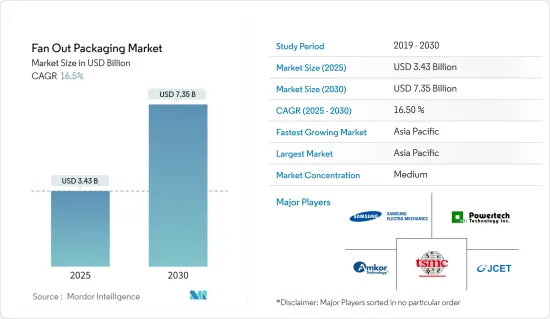
The Fan Out Packaging Market size is estimated at USD 3.43 billion in 2025, and is expected to reach USD 7.35 billion by 2030, at a CAGR of 16.5% during the forecast period (2025-2030).
The expansion of this market is being driven by technological advancements in semiconductor-based technologies and rapidly expanding demand in various sectors.
Key Highlights
- Fan-out wafer level packaging (FOWLP) finds its increased application in footprint-sensitive devices such as smartphones due to the requirement of high-performing, energy-efficient thin- and small-form-factor packages. Further, on average, five to seven wafer-level packages (especially fan-out) can be found in modern smartphones, and the numbers are expected to increase in the future. This is because they are gradually replacing the more traditional package-on-package (PoP) memory-on-logic solutions.
- Moreover, the increasing application of artificial intelligence and machine learning in various fields has increased the installation of high-performance computing in the market. UHD fan-out technology is expected to be applied to the cloud, 5G, autonomous cars, and AI chips and will lead the packaging trend during the forecast period.
- South Korea's semiconductor industry is continuing to put in efforts to improve and make 3D TSV (Through-silicon via), packaging and FoWLP (Fan-out Wafer-Level Packaging), and FoPLP (Fan-out Panel-Level Packaging) technologies more effective to raise the performance of semiconductors and the degree of integration.
- In December 2021, Nepes Laweh corporation announced the successful production of the world's first 600 mm x 600 mm large Panel Level Packaging (PLP) using Deca's M-Series fan-out technologies. The Fan-out-Panel Level Packaging (FOPLP) line passed customer certification in the third quarter, established a consistent yield, and commenced full-scale mass production, according to the business.
- Because South Korean companies depended on foreign companies for these systems in the past, KOSTEK is expecting a huge import substitution effect in the future. Its temporary wafer bonder and debonding techniques can be used during a fan-out packaging process.
- With the outbreak of COVID-19, the semiconductor packaging market witnessed a decline in growth due to restrictions on the movement of goods and severe disruptions in the semiconductor supply chain. In Q1 2020, COVID-19 caused low inventory levels for clients of semiconductor vendors and distribution channels. The market is expected to witness a long-term impact due to the coronavirus outbreak.
Fan Out Packaging Market Trends
High-Density Fan-Out to Hold a Significant Share
- Targeted for mid-range to high-end apps, high-density fan-out has between 6 to 12 I/Os per mm2 and between 15/15 μm to 5/5 μm line/space. High-density fan-out packaging gained popularity to address the form factor and performance requirements for mobile phone packaging. Key building blocks for this technology comprise redistribution layer (RDL) metal and mega pillar plating.
- TSMC's InFO technology is one of the most notable examples of high-density fan-out. This technology targets higher pin count applications, such as application processors (AP). The company plans to extend its FO-WLP segment into technologies like inFO-Antenna-in-Package (AiP) and inFO-on-Substrate. These packages are used in automobiles, servers, and smartphones. Apple was one of the early adopters of this new technology, which used it in the A10 application processor of the iPhone 7, introduced in late 2016.
- Owing to such benefits, in December 2021, Qualcomm and MediaTek both considered adopting fan-out PoP in the production of their flagship smartphone application processors, following in the footsteps of Apple utilizing TSMC's InFO_PoP technology to package its iPhone chips.
- Furthermore, semiconductor market growth along with development in high-density fan-out packaging solutions is expected to propel market growth over the forecast period. For instance, in July 2021, Changdian Technology, the world's premier combined circuit manufacturer and technology solution provider, revealed the official introduction of the entire line of very high-density fan-out packaging options for XDFOI chips, that are intended to deliver cost-effective, high-density connectivity, high-integration, and high-reliability solutions for chip heterogeneous integration.
- Advancements are also made in the fabrication method of manufacturing High-Density Fan-Out Wafer Level Packaging (FOWLP). Solutions are being developed to reduce chip size/height and lower production costs while improving reliability, energy efficiency, device speed, and multi-function integration. For instance, SPTS Technologies offers multiple plasma etch and deposition process technologies to leading semiconductor packaging companies for advanced packaging schemes such as that of high-density fan-out wafer-level packaging.
- Moreover, high-density fan-out (HDFO) packages can address these needs of miniaturization by fabrication capabilities of wafer-level processing coupled with its ability to create 3D structures using through-mold interconnects such as tall copper (Cu) pillars and through package vias (TPVs) and advanced flip chip packaging technologies.
Taiwan to Hold a Significant Share in the Market
- Taiwan houses some of the major semiconductor manufacturing companies which are fueling the demand for advanced semiconductor packaging, especially in PLPs. According to a government think tank, Science and Technology International Strategy Center, Taiwan's output was expected to grow by 25.9% in 2021 to USD 147 billion.
- According to the Semiconductor Industry Association (SIA), Asia-Pacific generates more than 50% of revenue for global semiconductor sales; this, in turn, provides Taiwanese vendors with an opportunity to supply FOWLP for increased semiconductor applications.
- Most of the companies in the country are expanding their production capacity of Fan-out packaging, which is further expected to increase exports and help develop the local market. For instance, Intel, which recently announced its return to the foundry industry, will simultaneously invest USD 3.5 billion in New Mexico to construct a semiconductor packaging factory that will begin operations in the second half of 2022.
- Further, in June 2021, ASE, a pure semiconductor post-processing (OAST), started investing in advanced packaging facilities in response to the supply and demand shortage of semiconductors. It is accelerating the expansion by purchasing a large amount of semiconductor manufacturing equipment for WLP and PLP processes from HANMI Semiconductor.
- Also, the growing market for fifth-generation (5G) wireless communication and high-performance computing has enabled manufacturers to develop newer technologies. For instance, as a sole leader in the High-Density Fan-out segment, TSMC is planning to extend its FO-WLP segment into technologies like inFO-Antenna-in-Package (AiP) and inFO-on-Substrate (oS).
Fan Out Packaging Industry Overview
The market is moderately fragmented, with the presence of numerous players. Some of the major players operating in the global fan-out packaging market include Taiwan Semiconductor Manufacturing Company Limited, Jiangsu Changjiang Electronics Tech Co., Amkor Technology Inc., Samsung Electro-Mechanics, and Powertech Technology Inc., among others. These players indulge in product innovation, mergers, and acquisitions, among other developments, in order to increase market share.
- November 2021 - Amkor Technology, Inc., a semiconductor packing and test service supplier, stated that it intends to construct an intelligent factory in Bac Ninh, Vietnam. The proposed factory's initial phase will concentrate on offering Advanced System in Package (SiP) assembling and testing services to the world's premier semiconductor and electronics manufacturing businesses.
- February 2021 - Samsung Foundry has filed documents with authorities in Arizona, New York, and Texas seeking to build a leading-edge semiconductor manufacturing facility in the USA. The potential fab near Austin, Texas, is expected to cost over USD 17 billion and create 1,800 jobs. It is expected to go online by the fourth quarter of 2023.
Additional Benefits:
- The market estimate (ME) sheet in Excel format
- 3 months of analyst support
TABLE OF CONTENTS
1 INTRODUCTION
- 1.1 Study Assumptions and Market Definition
- 1.2 Scope of the Study
2 RESEARCH METHODOLOGY
3 EXECUTIVE SUMMARY
4 MARKET INSIGHTS
- 4.1 Market Overview
- 4.2 Industry Attractiveness - Porter's Five Forces Analysis
- 4.2.1 Bargaining Power of Suppliers
- 4.2.2 Bargaining Power of Buyers
- 4.2.3 Threat of New Entrants
- 4.2.4 Intensity of Competitive Rivalry
- 4.2.5 Threat of Substitute Products
- 4.3 Impact of COVID-19 on the Market
5 MARKET DYNAMICS
- 5.1 Market Drivers
- 5.1.1 The Proliferation of 5G Wireless Networking Along with High-performance Computing
- 5.2 Market Restraints
- 5.2.1 Manufacturing And Cost Challenges Associated with Production
- 5.3 Market Opportunities for FOPLP
- 5.4 Impact of COVID-19 on the market
6 MARKET SEGMENTATION
- 6.1 By Type
- 6.1.1 Core Fan-Out
- 6.1.2 High-Density Fan-Out
- 6.1.3 Ultra High-density Fan Out
- 6.2 By Carrier Type
- 6.2.1 200 mm
- 6.2.2 300 mm
- 6.2.3 Panel
- 6.3 By Business Model
- 6.3.1 OSAT
- 6.3.2 Foundary
- 6.3.3 IDM
- 6.4 Geography
- 6.4.1 Taiwan
- 6.4.2 China
- 6.4.3 United States
- 6.4.4 South Korea
- 6.4.5 Japan
- 6.4.6 Europe
7 FAN-OUT PACKAGING VENDOR RANKING ANALYSIS
8 COMPETITIVE LANDSCAPE
- 8.1 Company Profiles
- 8.1.1 Taiwan Semiconductor Manufacturing Company Limited
- 8.1.2 Jiangsu Changjiang Electronics Tech Co.
- 8.1.3 Samsung Electro-Mechanics
- 8.1.4 Powertech Technology Inc.
- 8.1.5 Amkor Technology Inc.
- 8.1.6 Advanced Semiconductor Engineering Inc
- 8.1.7 Nepes Corporation
