
|
市場調査レポート
商品コード
1630382
感光性半導体デバイス:市場シェア分析、産業動向・統計、成長予測(2025~2030年)Photosensitive Semiconductor Device - Market Share Analysis, Industry Trends & Statistics, Growth Forecasts (2025 - 2030) |
||||||
カスタマイズ可能
適宜更新あり
|
|||||||
| 感光性半導体デバイス:市場シェア分析、産業動向・統計、成長予測(2025~2030年) |
|
出版日: 2025年01月05日
発行: Mordor Intelligence
ページ情報: 英文 120 Pages
納期: 2~3営業日
|

全表示
- 概要
- 目次
概要
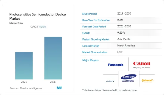
感光性半導体デバイス市場は予測期間中にCAGR 9.2%を記録する見込みです。
主なハイライト
- フォトダイオードセンサは、医療用イメージング、分光、パルスオキシメトリなどの医療機器や科学機器に幅広く使用されており、同市場の成長を牽引すると期待されています。
- さらに、イメージセンサの感光性半導体デバイスは、その応用領域を大幅に拡大しています。例えば、CMOS技術は、電子機器メーカーがデバイス設計を改善し、マーケットプレースで製品を差別化し、特定の消費者ニーズを満たすために活用する多くの利点を提供します。したがって、イメージセンサの成長は、市場における感光性半導体デバイスの成長を後押しします。
- 中国、インド、韓国、台湾、日本のようなアジア諸国は、これらのデバイス・メーカーの存在感が大きく、COVID-19の間にロックダウンや生産スケジュールの中断を経験しました。ほとんどの世界経済が封鎖された結果、納品は必需品に限られ、企業収益目標も修正されたため、この時期の売上は減少しました。ウイルスが蔓延する中、世界各国の政府が家電製品の製造工程の閉鎖と停止を命じたため、この時期の感光性半導体デバイス市場はマイナスの影響を受けました。しかし、様々な産業、組織、学校、大学によるヘルスケア機器やオンライン作業・学習の利用は、市場の着実な成長につながった。
感光性半導体デバイス市場動向
民生用電子機器セグメントが最大の市場シェアを占める見込み
- 感光性半導体デバイスは、主に多くのイメージングデバイスやデジタルカメラでイメージセンサとして使用され、画像の焼灼や保存の質を高めています。これらの画像アプリケーションは、産業、メディア、医療、民生アプリケーションで高い採用率を誇っています。
- スマートフォン、セキュリティカメラ、高解像度カメラ、カムコーダの需要が増加しているため、感光性半導体デバイス市場は予測期間中にさらに成長すると予想されます。世界のメーカーは、解像度、性能、ピクセルサイズなどの主要パラメータの向上に努めています。
- さらに、CMOSセンサーにおける感光性半導体デバイスの使用の増加は、カメラ設計を簡素化するオンチップにより多くの機能を提供することで、民生市場の低コストエンドに足掛かりを提供しています。例えば、ソニーが新たに発売したIMX686 Exmor RS 64MP CMOSセンサーは、サムスン、ファーウェイ、OnePlus、シャオミなどの多くのミッドレンジスマホに採用されています。
- しかし、各業界の企業が経験した大幅な景気後退のため、従業員の給与も削減されています。これは、感光性半導体デバイスで設計された家電製品の購入決定に直接影響を与え、短期的に市場の成長に影響を与える可能性があります。
アジア太平洋地域が最も急成長する見込み
- 同地域全体では、中間層によるスマートフォン、タブレット、テレビなどの家電製品への支出が増加しており、これが家電市場の成長を牽引し、同地域における感光性半導体デバイスの成長を導いています。
- 多くの企業がこの地域で新技術を採用し、市場を牽引できる開発を行っています。例えば、2022年5月、三菱電機株式会社は、同社が宇宙空間の真空中で衛星アンテナの3Dプリンティングのために感光性樹脂と太陽紫外線を使用する軌道上付加製造技術を開発したと発表しました。
- さらに、2022年1月。東レはネガ型感光性ポリイミド材料を開発したと発表しました。この新製品は、ポリイミドの特徴である耐熱性、機械特性、接着性を維持しながら、解像度を高め、100マイクロメートルやその他の厚膜への高精細パターン形成を可能にします。そして、これが市場を大きく牽引すると思われます。
- 同地域の軍隊のインフラ開発への投資が多いことも、市場の成長を後押ししています。例えば、公式文書や軍事情報源によると、インドは2022-23年に187億6,000万米ドルを国防と軍隊に費やしており、軍隊を更新し、地域のライバルに対する戦闘能力を強化するために、今後さらに増加すると予想されています。このような投資は監視装置の需要を高め、ひいてはこの地域の感光性半導体デバイスの成長を後押しします。
感光性半導体デバイス産業の概要
感光性半導体デバイスの世界市場は非常に細分化されており、複数のメーカーが製品を提供しています。各社は、より良い製品をより低価格で消費者に提供するため、製品や技術に継続的に投資しています。また、各社は市場シェアを拡大するため、特にこれらの製品を扱う企業を買収しています。
- 2022年9月- 富士フイルム株式会社は、ミラーレスデジタルカメラ「FUJIFILM X-H2」の発売を発表しました。同社は、小型軽量カメラ「Xシリーズ」の最新ラインアップとしています。また、新開発の裏面照射型40.2MP X-Trans CMOS 5 HRセンサーと、高解像度の静止画と高精細な8K/30P動画の撮影が可能な高速X-Processor 5を搭載しているといいます。
- 2021年12月- キヤノン株式会社は、セキュリティカメラ用3.2MP SPADセンサーの量産を2022年に開始すると発表しました。同社によると、SPADセンサーは、各画素に電子素子を搭載した独自設計のイメージセンサーです。CMOSセンサーでは、蓄積された電子電荷の読み出しに電子ノイズが含まれ、蓄積光の測定方法によって画質が低下します。一方、SPADセンサーでは、ノイズが光を電気信号として読み出すことを妨げないため、信号ノイズのない鮮明な被写体の撮影が可能となり、撮影時の高感度化や高精度な測距などのメリットが得られます。
その他の特典:
- エクセル形式の市場予測(ME)シート
- 3ヶ月間のアナリストサポート
目次
第1章 イントロダクション
- 調査の前提条件と市場定義
- 調査範囲
第2章 調査手法
第3章 エグゼクティブサマリー
第4章 市場力学
- 市場概要
- 産業バリューチェーン分析
- 業界の魅力度-ポーターのファイブフォース分析
- 供給企業の交渉力
- 消費者の交渉力
- 新規参入業者の脅威
- 代替品の脅威
- 競争企業間の敵対関係
- 市場促進要因
- イメージングと光学センシングソリューションの改善需要
- 長寿命と低消費電力
- 市場抑制要因
- 価格圧力の高まり
- COVID-19の業界への影響評価
第5章 市場セグメンテーション
- デバイス別
- フォトセル
- フォトダイオード
- フォトトランジスタ
- フォトレジスタ
- フォトIC
- エンドユーザー別
- 自動車・輸送機器
- 民生用電子機器
- 航空宇宙・防衛
- ヘルスケア
- 産業
- セキュリティーとセキュリティ
- 地域別
- 北米
- 欧州
- アジア太平洋
- ラテンアメリカ
- 中東・アフリカ
第6章 競合情勢
- 企業プロファイル
- Sony Corporation
- Samsung Electronics Co. Ltd
- Canon Inc.
- SK Hynix Inc.
- Fujifilm
- Panasonic Corporation
- Continental AG
- Robert Bosch GmbH
- Denso Corporation
- Teledyne Technologies Inc.
- Hamamatsu Photonics K.K.
第7章 投資分析
第8章 市場機会と今後の動向
目次
Product Code: 70354
The Photosensitive Semiconductor Device Market is expected to register a CAGR of 9.2% during the forecast period.
Key Highlights
- The extensive use of photodiode sensors in medical products for medical imaging, spectroscopy, and pulse oximetry, among other medical and scientific instrumentations, is expected to drive the growth of the photodiode in the market.
- Moreover, photosensitive semiconductor devices in image sensors have immensely increased their application area. For instance, CMOS technology offers plenty of benefits that electronics manufacturers leverage to improve device design, differentiate their products in the marketplace, and meet specific consumer needs. Therefore, the growth of image sensors will boost the growth of photosensitive semiconductor devices in the market.
- Asian countries like China, India, South Korea, Taiwan, and Japan have a significant presence of manufacturers of these devices and had experience lockdowns and disrupted production schedules during Covid-19. The sales went down during that period as the lockdown in most global economies had resulted in deliveries limited to essentials and companies revising their revenue targets. Amid the spread of viruses, governments worldwide mandated the lockdown and halt of consumer electronics manufacturing processes, negatively impacting the photosensitive semiconductor device market during that period. However, the use of healthcare devices and online working and study opted by various industries, organizations, schools, and colleges led to a steady growth in the market.
Photosensitive Semiconductor Device Market Trends
Consumer Electronic Segment is Expected to Hold Largest Market Share
- Photosensitive semiconductor devices are primarily used as image sensors in many imaging devices and digital cameras to enhance the quality of cauterization and storage of images. These imaging applications have high adoption in industrial, media, medical, and consumer applications.
- Due to the increasing demand for smartphones, security cameras, high-definition cameras, and camcorders, the photosensitive semiconductor device market is expected to grow more during the forecast period. Manufacturers worldwide strive to enhance main parameters, such as resolution, performance, and pixel size.
- Additionally, the increase in the use of photosensitive semiconductor devices in CMOS sensors is providing a foothold at the low-cost end of the consumer market by offering more functions on-chip that simplify camera design. For instance, Sony's newly launched IMX686 Exmor RS 64MP CMOS sensors are being used in many mid-range phones of Samsung, Huawei, OnePlus, Xiaomi, etc.
- However, due to the vast economic downturn experienced by companies across industries, employees are also witnessing salary cuts. This may directly impact the purchase decision for consumer electronics designed with photosensitive semiconductor devices and affect the growth of the market on a short-term basis.
Asia Pacific is Expected to be the Fastest growing Region
- Across the region, there is an increase in spending by the middle class on consumer electronics products such as smartphones, tablets, televisions, etc., which is driving the consumer electronics market growth and guiding the growth of photosensitive semiconductor devices in the region.
- Many companies are using new technologies and development in the region that can drive the market. For instance, in May 2022, Mitsubishi Electric Corporation announced that the company had developed an on-orbit additive-manufacturing technology that uses photosensitive resin and solar ultraviolet light for the 3D printing of satellite antennas in the vacuum of outer space.
- Additionally, in January 2022. Toray Industries, Inc. announced that the company had developed a negative photosensitive polyimide material. This new offering maintains polyimides' characteristic thermal resistance, mechanical properties, and adhesiveness while increasing resolutions and enabling high-definition pattern formation on 100-micrometer and other thick films. And that will drive the market significantly.
- The high investments in developing the infrastructure of armed forces in the region have boosted the market's growth. For instance, according to an official document and military sources, India has spent USD 18.76 billion in the year 2022-23 on its defense and armed forces, which is expected to increase more in the future to update the armed forces and reinforce their combat capacities over regional rivals. These investments will increase the demand for surveillance equipment, which will, in turn, boost the growth of photosensitive semiconductor devices in the area.
Photosensitive Semiconductor Device Industry Overview
The Global Photosensitive Semiconductor Device Market is highly fragmented, having multiple manufacturers providing the product. Companies continuously invest in products and technology to encourage better products at lower prices for their consumers. The companies are also acquiring companies that specifically deal with these products to boost their market share.
- September 2022 - FUJIFILM Corporation announced the launch of the mirrorless digital camera 'FUJIFILM X-H2'. The company stated it as the latest addition to the X Series of compact, lightweight cameras lineup. Moreover, they also said that the camera features the new back-illuminated 40.2MP X-Trans CMOS 5 HR sensor and the high-speed X-Processor 5 capable of capturing high-resolution stills and high-definition 8K/30P video.
- December 2021 - Canon Inc. announced to start of mass production of the 3.2MP SPAD sensor for security cameras in 2022. As per the company, the SPAD sensor is a uniquely designed image sensor with each pixel possessing an electronic element. With CMOS sensors, the readout of the accumulated electronic charge contains electronic noise, which diminishes image quality due to how accumulated light is measured. Meanwhile, with SPAD sensors, noise does not interfere with the readout of light as electrical signals, which enables clear image capture of subjects free from signal noise and provides advantages such as greater sensitivity during image capture and high-precision distance measurement.
Additional Benefits:
- The market estimate (ME) sheet in Excel format
- 3 months of analyst support
TABLE OF CONTENTS
1 INTRODUCTION
- 1.1 Study Assumptions and Market Definition
- 1.2 Scope of the Study
2 RESEARCH METHODOLOGY
3 EXECUTIVE SUMMARY
4 MARKET DYNAMICS
- 4.1 Market Overview
- 4.2 Industry Value Chain Analysis
- 4.3 Industry Attractiveness - Porter's Five Forces Analysis
- 4.3.1 Bargaining Power of Suppliers
- 4.3.2 Bargaining Power of Consumers
- 4.3.3 Threat of New Entrants
- 4.3.4 Threat of Substitutes
- 4.3.5 Intensity of Competitive Rivalry
- 4.4 Market Drivers
- 4.4.1 Demand for Improved Imaging and Optical Sensing Solutions
- 4.4.2 Long Life and Low Power Consumption
- 4.5 Market Restraints
- 4.5.1 Increasing Price Pressure
- 4.6 Assessment of Impact of Covid-19 on the Industry
5 MARKET SEGMENTATION
- 5.1 Device
- 5.1.1 Photocell
- 5.1.2 Photodiode
- 5.1.3 Phototransistor
- 5.1.4 Photoresistor
- 5.1.5 Photo IC
- 5.2 End User
- 5.2.1 Automotive and Transportation
- 5.2.2 Consumer Electronics
- 5.2.3 Aerospace and Defence
- 5.2.4 Healthcare
- 5.2.5 Industrial
- 5.2.6 Security and Survelliance
- 5.3 Geography
- 5.3.1 North America
- 5.3.2 Europe
- 5.3.3 Asia Pacific
- 5.3.4 Latin America
- 5.3.5 Middle East and Africa
6 COMPETITIVE LANDSCAPE
- 6.1 Company Profiles
- 6.1.1 Sony Corporation
- 6.1.2 Samsung Electronics Co. Ltd
- 6.1.3 Canon Inc.
- 6.1.4 SK Hynix Inc.
- 6.1.5 Fujifilm
- 6.1.6 Panasonic Corporation
- 6.1.7 Continental AG
- 6.1.8 Robert Bosch GmbH
- 6.1.9 Denso Corporation
- 6.1.10 Teledyne Technologies Inc.
- 6.1.11 Hamamatsu Photonics K.K.
