
|
市場調査レポート
商品コード
1630220
メモリパッケージング:市場シェア分析、産業動向と統計、成長予測(2025~2030年)Memory Packaging - Market Share Analysis, Industry Trends & Statistics, Growth Forecasts (2025 - 2030) |
||||||
カスタマイズ可能
適宜更新あり
|
|||||||
| メモリパッケージング:市場シェア分析、産業動向と統計、成長予測(2025~2030年) |
|
出版日: 2025年01月05日
発行: Mordor Intelligence
ページ情報: 英文 120 Pages
納期: 2~3営業日
|

全表示
- 概要
- 目次
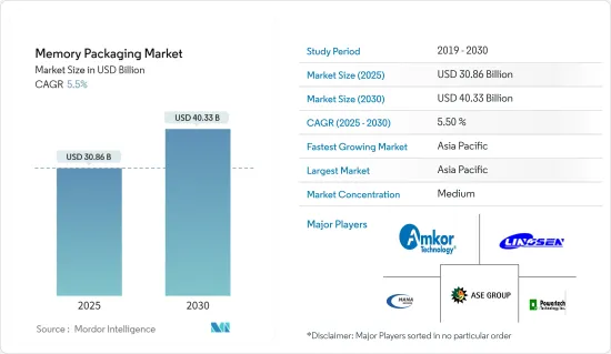
メモリパッケージングの市場規模は2025年に308億6,000万米ドルと推計され、予測期間(2025-2030年)のCAGRは5.5%で、2030年には403億3,000万米ドルに達すると予測されます。
最近のCOVID-19の流行は、アジア太平洋、特に中国が調査対象市場の主要な影響要因の一つであることから、調査対象市場のサプライチェーンに大きな不均衡をもたらすと予想されます。また、アジア太平洋の地方政府の多くは、長期的なプログラムで半導体産業に投資しており、それ故に市場の成長を取り戻すと期待されています。例えば、中国政府は国家IC投資基金2030の第2フェーズに約230億~300億米ドルの資金を調達しました。パンデミックからの市場の回復時間が不透明なため、世界のいくつかの地域への経済的影響は、半導体市場の成長に大きな課題を提供し、先進メモリパッケージング市場に必要な重要な原材料の入手可能性に世界的に直接影響を与えると予想されます。
主なハイライト
- メモリデバイスは、フリップチップ、リードフレーム、ワイヤーボンド、スルーシリコン・ビア(TSV)など、幅広いパッケージング技術を採用しています。チップの小型化と高機能化に伴い、外部回路との電気的接続の数が増えています。
- これはパッケージング技術の開発にもつながっています。フリップチップ、TSV、ウエハーレベル・チップスケール・パッケージング(WLCSP)は、広帯域化、高速化、パッケージの小型化・薄型化を満たす有望な技術です。分かりやすいプログラム調整、低エンジニアリングコスト、容易な切り替えが、ワイヤボンドメモリパッケージングプラットフォームへの需要を後押ししています。
- さらに、パッケージング設計の変化により、ワイヤーボンド・メモリパッケージング・プラットフォームは、その柔軟性、信頼性、低コストにより、最も好まれる相互接続プラットフォームとして使用され続けています。フリップチップは、2016年にDRAMメモリパッケージングへの進出を開始し、高帯域幅要件に後押しされたDRAM PC/サーバーでの採用増加により成長が見込まれています。
- 高帯域幅とメモリチップの低レイテンシは、多くのアプリケーションで高性能コンピューティングへの要求に拍車をかけており、シリコン貫通電極(TSV)が高帯域幅メモリデバイスに採用されています。
メモリパッケージング市場動向
DRAMが大きなシェアを占めると予測
- 同市場は、モバイルとコンピューティング(主にサーバー)からの需要を目の当たりにしています。スマートフォン1台当たりのDRAMメモリ容量は、平均で3倍以上に増加し、2022年には約6GBに達すると予想されています。
- 最近、調査対象市場の支配的プレーヤーの1つであるサムスン電子が、ハイエンド・スマートフォン向けの新しいメモリパッケージングの量産を発表しました。
- モバイル・アプリケーションでは、メモリパッケージングはワイヤー・ボンド・プラットフォームが主流であると予想されます。しかし、ハイエンドスマートフォン向けのマルチチップパッケージング(ePoP)への移行が間もなく始まると思われます。エンタープライズアーキテクチャやクラウドコンピューティングの向上に伴い、コンピューティングDRAMパッケージングは予測期間中に大きな成長を遂げると予想されます。
- サムスンのHBM2テクノロジーは、8個の8GビットDRAMダイで構成され、5,000個のTSVを使用して積層接続されます。最近、同社は12個のDRAMダイを積層し、6万個のTSVを使用して接続された新しいHBMバージョンも発表しました。
- スマートフォン1台当たりのDRAMメモリ容量は増加しており、新しいデバイスは最低4Gbの容量を提供し、2020年には最低6GBから8GBの容量に達すると予想されています。スマートフォン1台当たりのNAND容量は増加しており、現在64GB以上、2020年には150GB以上に達すると予想されています。サーバ向けでは、1台あたりのDRAM容量は2020年までに約1TBに増加し、エンタープライズ向けSSDのNAND容量は予測期間末までに5TB以上に達すると予測されます。
自動車産業が大きなシェアを占める
- 低密度(低MB)メモリを使用する自動車市場では、自律走行や車載インフォテインメントの動向に牽引され、DRAMメモリの採用が増加する可能性があります。NORフラッシュメモリパッケージング市場も、タッチディスプレイ・ドライバIC、AMOLEDディスプレイ、産業用IoTなどの新分野への応用により成長が見込まれています。
- 成長戦略の一環として、多数のOSATプレーヤーがメモリチップメーカーと戦略的提携を結んでおり、地域プレーヤーは世界技術プロバイダーと提携して市場でのリーチを拡大しています。
- 同市場で事業を展開するメーカーは、生産施設を拡張しています。例えば、SK Hynix Inc.は韓国で半導体パッケージングと検査施設の能力を拡大しています。このような開発により、既存プレーヤーは市場開拓の機会を増やし、競合他社は市場で優位に立つことができると思われます。
- パッケージング技術に導入されている技術革新は、大型システムオンチップ(SoC)ソリューションの機能密度の増加に関連しています。しかし、自動車環境における厳しい信頼性要件やOSATs業界の情勢の変化が、予測期間中の市場成長の妨げになると予想されます。
- 最近では、バイオメトリックセンサ、CMOSイメージセンサ、加速度計などのMEMSセンサなど、さまざまな用途でSiベースのセンサ技術の使用が増加しています。また、携帯電話やPDAなどの携帯機器に組み込まれるセンサ・デバイスも増えています。これらのアプリケーションでは、このセンサー技術をうまく組み込むために、小型、低コスト、組み込みやすさが不可欠です。
- 一般的に、OEMはプラグアンドプレイモジュールまたは完全なサブシステムを好むが、これもメモリチップ市場を助ける要因であり、ひいては技術的応用を強化するためのメモリパッケージング需要を牽引しています。
メモリパッケージング業界の概要
メモリパッケージング市場の競争は中程度です。DRAMメモリの価格高騰に伴い、メモリパッケージング市場で事業を展開するベンダーは、3D NANDの開発への支出を増やしています。SK Hynix Inc.が発表した記事によると、各社はもはや3D NANDの需要についていけず、製造能力の拡張を求められています。また、多くの企業が需要の増加に対応するために製造装置を拡張しています。全体として、予測期間中、市場は上記のすべての要因のために高度な競争へと移行する可能性があります。
その他の特典:
- エクセル形式の市場予測(ME)シート
- 3ヶ月間のアナリストサポート
目次
第1章 イントロダクション
- 調査の前提条件と市場定義
- 調査範囲
第2章 調査手法
第3章 エグゼクティブサマリー
第4章 市場力学
- 市場概要
- 業界の魅力度-ポーターのファイブフォース分析
- 供給企業の交渉力
- 消費者の交渉力
- 新規参入業者の脅威
- 代替品の脅威
- 競争企業間の敵対関係
- 産業バリューチェーン分析
- 技術ロードマップ
- COVID-19の市場への影響評価
- 市場促進要因
- 自律走行と車載インフォテインメントの新たな動向
- スマートフォン需要の増加
- メモリ半導体ビジネスの爆発的成長
- 高帯域幅メモリ(HBM)と再分配層の継続的開発
- 市場の課題
- 車載環境における厳しい信頼性要件
- OSAT業界情勢の変化
第5章 市場セグメンテーション
- プラットフォーム別
- フリップチップ
- リードフレーム
- ウエハーレベル・チップスケール・パッケージング(WLCSP)
- シリコン貫通電極(TSV)
- ワイヤーボンド
- 用途別
- NANDフラッシュパッケージング
- NORフラッシュパッケージング
- DRAMパッケージング
- その他のアプリケーション
- エンドユーザー産業別
- ITおよびテレコム
- コンシューマー・エレクトロニクス
- 自動車
- その他のエンドユーザー産業
- 地域別
- 北米
- 欧州
- アジア太平洋
- 世界のその他の地域
第6章 競合情勢
- 企業プロファイル
- Tianshui Huatian Technology Co. Ltd
- Hana Micron Inc.
- Lingsen precision industries Ltd
- Formosa Advanced Technologies Co. Ltd(Nanya Technology Corporation)
- Advanced Semiconductor Engineering Inc.(ASE Inc.)
- Amkor Technology Inc.
- Powertech Technology Inc.
- Jiangsu Changjiang Electronics Technology Co. Ltd
- Powertech Technology Inc.
- King Yuan Electronics Corp. Ltd
- ChipMOS Technologies Inc.
- TongFu Microelectronics Co.
- Signetics Corporation
第7章 投資分析
第8章 市場の将来
The Memory Packaging Market size is estimated at USD 30.86 billion in 2025, and is expected to reach USD 40.33 billion by 2030, at a CAGR of 5.5% during the forecast period (2025-2030).
The recent COVID-19 outbreak is expected to create significant imbalances in the supply chain of the market studied, as Asia-Pacific, particularly China, is one of the major influencers of the market studied. Also, many of the local governments in the Asia-Pacific have invested in the semiconductor industry in a long run program, hence, expected to regain market growth. For instance, the Chinese government raised around USD 23 to 30 billion funds, to pay for the second phase of its National IC Investment Fund 2030. Owing to the uncertainty in the recovery time of the market from the pandemic, economic impacts on several parts of the world are further expected to provide significant challenges to the growth of the semiconductor market, directly affecting the availability of critical raw materials required for advanced memory packaging market globally.
Key Highlights
- Memory devices employed a broad range of the packaging technology that include flip-chip, lead-frame, wire-bond, through-silicon via (TSV). With the decrease in dimensions and increase in the chip functionality, a higher number of the electrical connections have to be made to the external circuit.
- This has also led to development in packaging technologies. Flip-chip, TSV, and wafer-level chip-scale Packaging (WLCSP) are promising technologies to satisfy wider bandwidth, faster speed, and smaller/thinner package. Comprehensible program adjustments, low engineering costs, and easy changeovers are fueling the demand for the wire-bond memory packaging platform.
- Additionally, due to changes in the package design, the wire-bond memory packaging platform continues to be used as the most preferred interconnection platform because of its flexibility, reliability, and low-cost. Flip-chip began making inroads in the DRAM memory packaging in 2016 and was expected to grow due to its increased adoption in the DRAM PC/server, fueled by high bandwidth requirements.
- Spurred on by high bandwidth and memory chips' low latency demands for high-performance computing in numerous applications, through-silicon via (TSV), is being employed in high bandwidth memory devices.
Memory Packaging Market Trends
DRAM is Estimated to Hold Significant Share
- The market studied is witnessing demand from mobile and the computing (mainly servers). On average, the DRAM memory capacity per smartphone is anticipated to rise more than threefold to reach around 6GB by 2022.
- Recently, Samsung Electronics Co. Ltd, one of the dominant players in the market studied, announced the mass production of the new memory package aimed at high-end smartphones, which may save space by putting DRAM and eMMC together.
- For mobile applications, memory packaging is expected to remain on the wire-bond platform mostly. However, it will soon begin moving toward the multi-chip package (ePoP) for high-end smartphones. With the improvement in enterprise architecture and cloud computing, the computing DRAM packaging is anticipated to witness significant growth during the forecast period.
- Samsung's HBM2 technology consists of eight 8Gbit DRAM dies, which are stacked and connected using 5,000 TSVs. Recently, the company also launched a new HBM version that stacks 12 DRAM dies, which are connected using 60,000 TSVs and are ideal for data-intensive applications, such as AI and HPC.
- DRAM memory capacity per smartphone has risen with new devices offering a minimum of 4 Gb space which is expected to reach a minimum of 6 GB to 8 GB of space by 2020, while NAND capacity per smartphone has increased reaching more than 64 GB now and are expected to become reach over 150 GB by 2020. For servers, DRAM capacity per unit is projected to increase to approximately 1 TB by 2020 and NAND capacity for each SSD for the enterprise market are expected to reach more than 5 TB in capacity by the end of the forecast period
Automotive Industry to Hold Significant Share
- The automotive market, which uses the low density (low-MB) memory, might observe an increase in the acceptance of DRAM memory, led by the growing trend of autonomous driving and in-vehicle infotainment. NOR Flash memory packaging market is also expected to grow due to its application in new areas, such as touch display driver ICs, AMOLED display, and industrial IoTs.
- As part of the growth strategy, numerous OSAT players are entering into strategic alliances with memory chip manufacturers, and regional players are partnering with global technology providers to increase their reach in the market.
- Manufacturers operating in the market are expanding their production facilities. For instance, SK Hynix Inc. is expanding its semiconductor packaging and inspection facility capacity in South Korea. Such developments are expected to help create increased opportunity for the existing players and cut competitors edge in the market studied.
- The innovations being introduced in the packaging technology are associated with the growth in functional density of large system-on-chip (SoC) solutions. However, harsh reliability requirements in the automotive environment and changing landscape of the OSATs industry is anticipated to hamper the growth of the market studied over the forecast period.
- In recent times, there has been growth in the use of Si-based sensor technology for a variety of applications, including biometric sensors, CMOS image sensors, and MEMS sensors, such as accelerometers. Increasingly, and sensor devices are being integrated into portable devices, like handsets and PDAs. In these applications, small-size, low-cost, and ease-of-integration are essential to incorporate this sensor technology successfully.
- Generally, OEMs prefer a plug-and-play module or complete subsystem, which is also a factor that is helping the memory chip market, and in turn, driving the demand for the memory packaging for enhanced technological applications.
Memory Packaging Industry Overview
The memory packaging market is moderately competitive. With the rising prices of DRAM memory, vendors operating in the memory packaging market are increasingly spending on the development of 3D NAND. According to an article published by SK Hynix Inc., companies can no longer keep up with 3D NAND demand and are required to expand their manufacturing capacity. Also, many of the companies are expanding their manufacturing units in order to meet the growing demand. Overall the market might move towards highly competitive during the forecast period due to all the above factors.
Additional Benefits:
- The market estimate (ME) sheet in Excel format
- 3 months of analyst support
TABLE OF CONTENTS
1 INTRODUCTION
- 1.1 Study Assumptions and Market Definition
- 1.2 Scope of the Study
2 RESEARCH METHODOLOGY
3 EXECUTIVE SUMMARY
4 MARKET DYNAMICS
- 4.1 Market Overview
- 4.2 Industry Attractiveness - Porter's Five Forces Analysis
- 4.2.1 Bargaining Power of Suppliers
- 4.2.2 Bargaining Power of Consumers
- 4.2.3 Threat of New Entrants
- 4.2.4 Threat of Substitutes
- 4.2.5 Intensity of Competitive Rivalry
- 4.3 Industry Value Chain AnalysiS
- 4.4 Technology RoadmaP
- 4.5 Assessment of Impact of COVID-19 on the Market
- 4.6 Market Drivers
- 4.6.1 Emerging Trend of Autonomous Driving and In-vehicle Infotainment
- 4.6.2 Increase in Demand for Smartphones
- 4.6.3 Memory Semiconductor Business Explosion
- 4.6.4 Continuous Developments in High-bandwidth Memory (HBM) and Redistribution Layer
- 4.7 Market Challenges
- 4.7.1 Harsh Reliability Requirements in the Automotive Environment
- 4.7.2 Changing Landscape of the OSATs Industry
5 MARKET SEGMENTATION
- 5.1 By Platform
- 5.1.1 Flip-chip
- 5.1.2 Lead-frame
- 5.1.3 Wafer-level Chip-scale Packaging(WLCSP)
- 5.1.4 Through-silicon Via (TSV)
- 5.1.5 Wire-bond
- 5.2 By Application
- 5.2.1 NAND Flash Packaging
- 5.2.2 NOR Flash Packaging
- 5.2.3 DRAM Packaging
- 5.2.4 Other Applications
- 5.3 By End-user Industry
- 5.3.1 IT and Telecom
- 5.3.2 Consumer Electronics
- 5.3.3 Automotive
- 5.3.4 Other End-user Industries
- 5.4 Geography
- 5.4.1 North America
- 5.4.2 Europe
- 5.4.3 Asia-Pacific
- 5.4.4 Rest of the World
6 COMPETITIVE LANDSCAPE
- 6.1 Company Profiles
- 6.1.1 Tianshui Huatian Technology Co. Ltd
- 6.1.2 Hana Micron Inc.
- 6.1.3 Lingsen precision industries Ltd
- 6.1.4 Formosa Advanced Technologies Co. Ltd (Nanya Technology Corporation)
- 6.1.5 Advanced Semiconductor Engineering Inc. (ASE Inc.)
- 6.1.6 Amkor Technology Inc.
- 6.1.7 Powertech Technology Inc.
- 6.1.8 Jiangsu Changjiang Electronics Technology Co. Ltd
- 6.1.9 Powertech Technology Inc.
- 6.1.10 King Yuan Electronics Corp. Ltd
- 6.1.11 ChipMOS Technologies Inc.
- 6.1.12 TongFu Microelectronics Co.
- 6.1.13 Signetics Corporation
