|
|
市場調査レポート
商品コード
1418248
半導体検査・測定装置市場レポート:2030年までの動向、予測、競合分析Semiconductor Inspection and Measurement Equipment Market Report: Trends, Forecast and Competitive Analysis to 2030 |
||||||
|
|
|||||||
カスタマイズ可能
適宜更新あり
|
|||||||


| 半導体検査・測定装置市場レポート:2030年までの動向、予測、競合分析 |
|
出版日: 2024年01月29日
発行: Lucintel
ページ情報: 英文 150 - page report
納期: 3営業日
|

- 全表示
- 概要
- 目次
半導体検査・測定装置の動向と予測
世界の半導体検査・測定装置市場は、2024年から2030年にかけてCAGR 5.0%で成長すると予測されます。この市場の主な促進要因は、モノのインターネット(IoT)、5G、人工知能を含む最先端技術の利用の拡大、半導体製造プロセスにおける高品質の検査・測定装置へのニーズの高まり、さらに品質管理の重視と生産コスト削減の要求の高まりです。世界の半導体検査・測定装置市場の将来は、ウエハー市場やマスク・フィルム市場における機会によって有望視されています。
半導体検査・測定装置市場の洞察
欠陥検査装置は、半導体のあらゆる欠陥や不規則性を探し出し検出するために作られ、欠陥のないデバイスだけが製造されることを保証するため、予測期間中に高い成長が見込まれると予測しています。
アジア太平洋は、特に中国やインドのような国々で半導体産業におけるアウトソーシング活動が増加しているため、予測期間中に最も高い成長が見込まれています。
よくある質問
Q1.市場の成長予測は?
A1.世界の半導体検査・測定装置市場は、2024年から2030年にかけてCAGR 5.0%で成長する見込みです。
Q2.市場の成長に影響を与える主な促進要因は?
A2.この市場の主な促進要因は、モノのインターネット(IoT)、5G、人工知能を含む最先端技術の利用拡大、半導体製造プロセスにおける高品質な検査・測定装置へのニーズの高まり、さらに品質管理の重視と生産コスト削減の要求の高まりです。
Q3.市場の主要セグメントは?
A3.世界の半導体検査・測定装置市場の将来は、ウエハー市場とマスク・フィルム市場に機会があり、有望です。
Q4. 市場の主要企業は?
A4. 半導体検査・測定装置の主要企業は以下の通りです。
- KLA
- Applied Materials
- Hitachi High-Technologies
- ASML
- Onto Innovation
- Lasertec
- SCREEN Semiconductor Solutions
- ZEISS
- Camtek
- Skyverse
Q5. 今後、最大となる市場セグメントは?
A5. 欠陥検査装置は、半導体のあらゆる欠陥や不規則性を探して検出し、欠陥のないデバイスだけが製造されることを保証するために作られるため、予測期間中に高い成長が見られる見通しです。
Q6. 市場において、今後5年間に最大になると予想される地域は?
A6. アジア太平洋は、特に中国やインドのような国々で半導体産業におけるアウトソーシング活動が増加しているため、予測期間中に最も高い成長が見込まれます。
Q7. レポートのカスタマイズは可能?
A7. はい、Lucintelは追加費用なしで10%のカスタマイズを提供します。
目次
第1章 エグゼクティブサマリー
第2章 世界の半導体検査・測定装置市場:市場力学
- イントロダクション、背景、分類
- サプライチェーン
- 業界の促進要因と課題
第3章 2018年から2030年までの市場動向と予測分析
- マクロ経済動向(2018~2023年)と予測(2024~2030年)
- 世界の半導体検査・測定装置の市場動向(2018~2023年)と予測(2024~2030年)
- タイプ別の世界の半導体検査・測定装置の市場
- 欠陥検査装置
- 計測機器
- 用途別の世界の半導体検査・測定装置市場
- ウエハー
- マスク/フィルム
第4章 2018年から2030年までの地域別の市場動向と予測分析
- 地域別の世界の半導体検査・測定装置市場
- 北米の半導体検査・測定装置市場
- 欧州の半導体検査・測定装置市場
- アジア太平洋の半導体検査・測定装置市場
- その他の地域 (ROW) の半導体検査・測定装置市場
第5章 競合の分析
- 製品ポートフォリオ分析
- 運用上の統合
- ポーターのファイブフォース分析
第6章 成長機会と戦略的分析
- 成長機会分析
- タイプ別の世界の半導体検査・測定装置市場の成長機会
- 用途別の世界の半導体検査・測定装置市場の成長機会
- 地域別の世界の半導体検査・測定装置市場の成長機会
- 世界の半導体検査・測定装置市場の新たな動向
- 戦略的分析
- 新製品の開発
- 世界の半導体検査・測定装置市場の生産能力拡大
- 世界の半導体検査・測定装置市場における合併、買収、合弁事業
- 認証とライセンシング
第7章 有力企業のプロファイル
- KLA
- Applied Materials
- Hitachi High-Technologies
- ASML
- Onto Innovation
- Lasertec
- SCREEN Semiconductor Solutions
- ZEISS
- Camtek
- Skyverse
Semiconductor Inspection and Measurement Equipment Trends and Forecast
The future of the global semiconductor inspection and measurement equipment market looks promising with opportunities in the wafer and mask/film markets. The global semiconductor inspection and measurement equipment market is expected to grow with a CAGR of 5.0% from 2024 to 2030. The major drivers for this market are growing use of cutting-edge technology including Internet of Things (IoT), 5G, and artificial intelligence, rising need for high-quality inspection and measurement equipment in the semiconductor manufacturing process, as well as, growing emphasis on quality control and the requirement to cut production costs.
A more than 150-page report is developed to help in your business decisions.
Semiconductor Inspection and Measurement Equipment by Segment
The study includes a forecast for the global semiconductor inspection and measurement equipment by type, application, and region.
Semiconductor Inspection and Measurement Equipment Market by Type [Shipment Analysis by Value from 2018 to 2030]:
- Defect Inspection Equipment
- Metrology Equipment
Semiconductor Inspection and Measurement Equipment Market by Application [Shipment Analysis by Value from 2018 to 2030]:
- Wafer
- Mask/Film
Semiconductor Inspection and Measurement Equipment Market by Region [Shipment Analysis by Value from 2018 to 2030]:
- North America
- Europe
- Asia Pacific
- The Rest of the World
List of Semiconductor Inspection and Measurement Equipment Companies
Companies in the market compete on the basis of product quality offered. Major players in this market focus on expanding their manufacturing facilities, R&D investments, infrastructural development, and leverage integration opportunities across the value chain. With these strategies semiconductor inspection and measurement equipment companies cater increasing demand, ensure competitive effectiveness, develop innovative products & technologies, reduce production costs, and expand their customer base. Some of the semiconductor inspection and measurement equipment companies profiled in this report include-
- KLA
- Applied Materials
- Hitachi High-Technologies
- ASML
- Onto Innovation
- Lasertec
- SCREEN Semiconductor Solutions
- ZEISS
- Camtek
- Skyverse
Semiconductor Inspection and Measurement Equipment Market Insights
Lucintel forecasts that defect inspection equipment is expected to witness higher growth over the forecast period because it is created to seek and detect any flaws or irregularities in semiconductors, guaranteeing that only devices free of flaws are manufactured.
APAC is expected to witness highest growth over the forecast period because of rise in outsourcing activities in the semiconductor industry, especially in countries like China and India.
Features of the Global Semiconductor Inspection and Measurement Equipment Market
Market Size Estimates: Semiconductor inspection and measurement equipment market size estimation in terms of value ($B).
Trend and Forecast Analysis: Market trends (2018 to 2023) and forecast (2024 to 2030) by various segments and regions.
Segmentation Analysis: Semiconductor inspection and measurement equipment market size by type, application, and region in terms of value ($B).
Regional Analysis: Semiconductor inspection and measurement equipment market breakdown by North America, Europe, Asia Pacific, and Rest of the World.
Growth Opportunities: Analysis of growth opportunities in different type, application, and regions for the semiconductor inspection and measurement equipment market.
Strategic Analysis: This includes M&A, new product development, and competitive landscape of the semiconductor inspection and measurement equipment market.
Analysis of competitive intensity of the industry based on Porter's Five Forces model.
FAQ
Q1. What is the growth forecast for semiconductor inspection and measurement equipment market?
Answer: The global semiconductor inspection and measurement equipment market is expected to grow with a CAGR of 5.0% from 2024 to 2030.
Q2. What are the major drivers influencing the growth of the semiconductor inspection and measurement equipment market?
Answer: The major drivers for this market are growing use of cutting-edge technology including Internet of Things (IoT), 5G, and artificial intelligence, rising need for high-quality inspection and measurement equipment in the semiconductor manufacturing process, as well as, growing emphasis on quality control and the requirement to cut production costs.
Q3. What are the major segments for semiconductor inspection and measurement equipment market?
Answer: The future of the global semiconductor inspection and measurement equipment market looks promising with opportunities in the wafer and mask/film markets.
Q4. Who are the key semiconductor inspection and measurement equipment market companies?
Answer: Some of the key semiconductor inspection and measurement equipment companies are as follows.
- KLA
- Applied Materials
- Hitachi High-Technologies
- ASML
- Onto Innovation
- Lasertec
- SCREEN Semiconductor Solutions
- ZEISS
- Camtek
- Skyverse
Q5. Which semiconductor inspection and measurement equipment market segment will be the largest in future?
Answer: Lucintel forecasts that defect inspection equipment is expected to witness higher growth over the forecast period because it is created to seek and detect any flaws or irregularities in semiconductors, guaranteeing that only devices free of flaws are manufactured.
Q6. In semiconductor inspection and measurement equipment market, which region is expected to be the largest in next 5 years?
Answer: APAC is expected to witness highest growth over the forecast period because of rise in outsourcing activities in the semiconductor industry, especially in countries like China and India.
Q7. Do we receive customization in this report?
Answer: Yes, Lucintel provides 10% customization without any additional cost.
This report answers following 11 key questions:
- Q.1. What are some of the most promising, high-growth opportunities for the semiconductor inspection and measurement equipment market by type (defect inspection equipment and metrology equipment), application (wafer and mask/film), and region (North America, Europe, Asia Pacific, and the Rest of the World)?
- Q.2. Which segments will grow at a faster pace and why?
- Q.3. Which region will grow at a faster pace and why?
- Q.4. What are the key factors affecting market dynamics? What are the key challenges and business risks in this market?
- Q.5. What are the business risks and competitive threats in this market?
- Q.6. What are the emerging trends in this market and the reasons behind them?
- Q.7. What are some of the changing demands of customers in the market?
- Q.8. What are the new developments in the market? Which companies are leading these developments?
- Q.9. Who are the major players in this market? What strategic initiatives are key players pursuing for business growth?
- Q.10. What are some of the competing products in this market and how big of a threat do they pose for loss of market share by material or product substitution?
- Q.11. What M&A activity has occurred in the last 5 years and what has its impact been on the industry?
Table of Contents
1. Executive Summary
2. Global Semiconductor Inspection and Measurement Equipment Market : Market Dynamics
- 2.1: Introduction, Background, and Classifications
- 2.2: Supply Chain
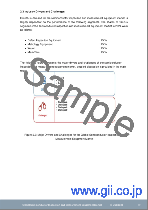
- 2.3: Industry Drivers and Challenges
3. Market Trends and Forecast Analysis from 2018 to 2030
- 3.1. Macroeconomic Trends (2018-2023) and Forecast (2024-2030)
- 3.2. Global Semiconductor Inspection and Measurement Equipment Market Trends (2018-2023) and Forecast (2024-2030)
- 3.3: Global Semiconductor Inspection and Measurement Equipment Market by Type
- 3.3.1: Defect Inspection Equipment
- 3.3.2: Metrology Equipment
- 3.4: Global Semiconductor Inspection and Measurement Equipment Market by Application
- 3.4.1: Wafer
- 3.4.2: Mask/Film
4. Market Trends and Forecast Analysis by Region from 2018 to 2030
- 4.1: Global Semiconductor Inspection and Measurement Equipment Market by Region
- 4.2: North American Semiconductor Inspection and Measurement Equipment Market
- 4.2.2: North American Semiconductor Inspection and Measurement Equipment Market by Application: Wafer and Mask/Film
- 4.3: European Semiconductor Inspection and Measurement Equipment Market
- 4.3.1: European Semiconductor Inspection and Measurement Equipment Market by Type: Defect Inspection Equipment and Metrology Equipment
- 4.3.2: European Semiconductor Inspection and Measurement Equipment Market by Application: Wafer and Mask/Film
- 4.4: APAC Semiconductor Inspection and Measurement Equipment Market
- 4.4.1: APAC Semiconductor Inspection and Measurement Equipment Market by Type: Defect Inspection Equipment and Metrology Equipment
- 4.4.2: APAC Semiconductor Inspection and Measurement Equipment Market by Application: Wafer and Mask/Film
- 4.5: ROW Semiconductor Inspection and Measurement Equipment Market
- 4.5.1: ROW Semiconductor Inspection and Measurement Equipment Market by Type: Defect Inspection Equipment and Metrology Equipment
- 4.5.2: ROW Semiconductor Inspection and Measurement Equipment Market by Application: Wafer and Mask/Film
5. Competitor Analysis
- 5.1: Product Portfolio Analysis
- 5.2: Operational Integration
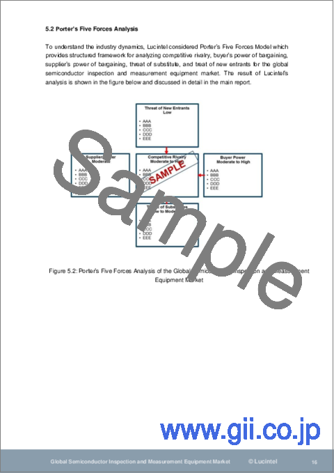
- 5.3: Porter's Five Forces Analysis
6. Growth Opportunities and Strategic Analysis
- 6.1: Growth Opportunity Analysis
- 6.1.1: Growth Opportunities for the Global Semiconductor Inspection and Measurement Equipment Market by Type
- 6.1.2: Growth Opportunities for the Global Semiconductor Inspection and Measurement Equipment Market by Application
- 6.1.3: Growth Opportunities for the Global Semiconductor Inspection and Measurement Equipment Market by Region
- 6.2: Emerging Trends in the Global Semiconductor Inspection and Measurement Equipment Market
- 6.3: Strategic Analysis
- 6.3.1: New Product Development
- 6.3.2: Capacity Expansion of the Global Semiconductor Inspection and Measurement Equipment Market
- 6.3.3: Mergers, Acquisitions, and Joint Ventures in the Global Semiconductor Inspection and Measurement Equipment Market
- 6.3.4: Certification and Licensing
7. Company Profiles of Leading Players
- 7.1: KLA
- 7.2: Applied Materials
- 7.3: Hitachi High-Technologies
- 7.4: ASML
- 7.5: Onto Innovation
- 7.6: Lasertec
- 7.7: SCREEN Semiconductor Solutions
- 7.8: ZEISS
- 7.9: Camtek
- 7.10: Skyverse