
|
市場調査レポート
商品コード
1721493
3Dスタッキングの市場機会、成長促進要因、産業動向分析、2025年~2034年予測3D Stacking Market Opportunity, Growth Drivers, Industry Trend Analysis, and Forecast 2025 - 2034 |
||||||
カスタマイズ可能
|
|||||||
| 3Dスタッキングの市場機会、成長促進要因、産業動向分析、2025年~2034年予測 |
|
出版日: 2025年04月01日
発行: Global Market Insights Inc.
ページ情報: 英文 180 Pages
納期: 2~3営業日
|

全表示
- 概要
- 目次
3Dスタッキングの世界市場は、2024年に18億米ドルとなり、CAGR21.1%で成長し、2034年までには118億米ドルに達すると予測されています。
この目覚ましい成長は、コンシューマエレクトロニクス、高性能コンピューティングシステム、先端半導体技術に対する需要の高まりによるところが大きいです。人工知能(AI)、機械学習、モノのインターネット(IoT)などのデータ集約型アプリケーションが拡大を続ける中、データ処理の高速化、効率の向上、電力管理の改善に対するニーズはこれまで以上に重要になっています。3Dスタッキングテクノロジーは、ロジック、メモリ、相互接続などの複数の機能レイヤーをコンパクトなフットプリント内に統合することで、デバイスメーカーがこうした進化するニーズに対応できるようにするもので、半導体イノベーションの将来を担うものとしてますます注目されています。エレクトロニクス業界が性能を犠牲にすることなく小型化を推し進める中、3Dスタッキングは、より高いスループット、より低いレイテンシ、優れた熱管理を実現する理想的な経路を提供します。スマートフォンやウェアラブルからデータセンタープロセッサや自律走行車まで、この技術の応用範囲は急速に拡大しています。チップレットベースの設計と異種集積の採用は、この市場の勢いをさらに加速させ、業界を問わず特定の使用事例向けにソリューションをカスタマイズできる柔軟性を提供します。
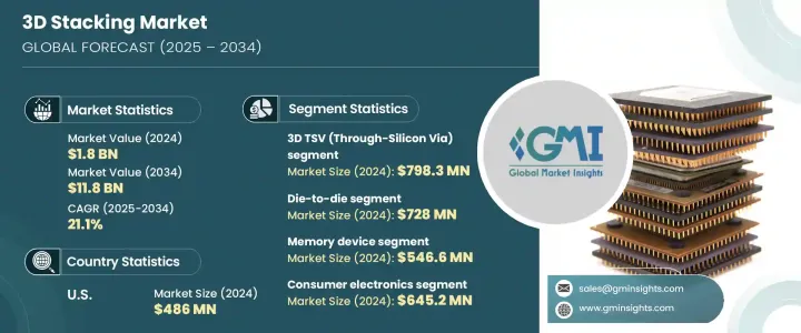
3Dスタッキング技術は、3Dハイブリッドボンディング、3D貫通電極(TSV)、モノリシック3D集積など、相互接続方式によって分類されます。このうち、3D TSV分野は2024年に7億9,830万米ドルを生み出しました。この分野は、データセンター、HPCプラットフォーム、自律システムの性能要件をサポートする高速、低レイテンシメモリインターフェイスに対する需要の高まりにより、力強い成長を遂げています。また、5Gネットワークの展開やスマートデバイスの普及により、膨大な量のリアルタイムデータ処理を管理できるエネルギー効率の高いコンパクトなチップアーキテクチャのニーズも高まっています。
| 市場範囲 | |
|---|---|
| 開始年 | 2024年 |
| 予測年 | 2025年~2034年 |
| 開始金額 | 18億米ドル |
| 予測金額 | 118億米ドル |
| CAGR | 21.1% |
同市場はさらに、ダイ・トゥー・ウェーハ、ウエハ・トゥー・ウェーハ、ダイ・トゥー・ダイ、チップ・トゥー・チップ、チップ・トゥー・ウェーハなどの相互接続技術別に区分されます。ダイ・トゥー・ダイの2024年の市場規模は7億2,800万米ドルでした。この手法は、ダイ間のシームレスな通信を必要とするマルチチップモジュールやチップセットベースのアーキテクチャに特に不可欠です。AIアクセラレータ、クラウドインフラ、HPCプロセッサの進歩に重要な役割を果たし、設計の柔軟性向上、省エネ強化、スケーラビリティ向上を実現します。
米国の3Dスタッキング市場は2024年に4億8,600万米ドルを創出しました。同地域は、AIアプリケーション、先進的データセンター運用、HPCインフラへの投資の増加により、大幅な成長を目の当たりにしています。米国の半導体企業は、次世代コンピューティングにおける性能、エネルギー効率、スケーラビリティの限界を押し広げるために、チップレットアーキテクチャやTSVベースの設計の開発にリソースを注いでいます。
世界の3Dスタッキング市場の主要企業には、AMD、ASE Technology Holding、Amkor Technology、Broadcom、IBM、Intel、Graphcore、JCET Group、Marvell Technology、Micron Technology、Kioxia、NVIDIA、OmniVision Technologies、SK Hynix、Sony Semiconductor Solutions、Samsung Electronics、SPIL、Western Digital、Xilinxなどがあります。これらの企業は、AI、データセンター、高性能コンピューティング市場からの需要拡大に対応するため、チップ積層と相互接続手法の革新を加速させています。集中的な研究開発と戦略的投資を通じて、電力効率、優れた性能、アーキテクチャの柔軟性を兼ね備えた、将来対応可能な半導体ソリューションを提供することを目指しています。
目次
第1章 調査手法と範囲
第2章 エグゼクティブサマリー
第3章 業界考察
- 業界エコシステム分析
- 業界への影響要因
- 成長促進要因
- 高性能コンピューティング(HPC)の需要の高まり
- AIとエッジコンピューティングのアプリケーションの拡大
- コンシューマーエレクトロニクスの成長
- 自動車・IoTアプリケーションの増加
- メモリとストレージの需要の増加
- 業界の潜在的リスク・課題
- 高い製造コスト・複雑性
- 熱と電力管理の問題
- 成長促進要因
- 成長可能性分析
- 規制情勢
- テクノロジーの情勢
- 将来の市場動向
- ギャップ分析
- ポーターの分析
- PESTEL分析
第4章 競合情勢
- イントロダクション
- 企業の市場シェア分析
- 主要市場企業の競合分析
- 競合ポジショニングマトリックス
- 戦略ダッシュボード
第5章 市場推計・予測:方法別、2021年~2034年
- 主要動向
- ダイ・トゥー・ダイ
- ダイ・トゥー・ウェーハ
- ウェーハ・トゥー・ウェーハ
- チップ間
- チップ・トゥー・ウェーハ
第6章 市場推計・予測:相互接続技術別、2021年~2034年
- 主要動向
- 3Dハイブリッドボンディング
- 3D TSV(シリコン貫通ビア)
- モノリシック3D統合
第7章 市場推計・予測:デバイスタイプ別、2021年~2034年
- 主要動向
- ロジックIC
- イメージング・オプトエレクトロニクス
- メモリデバイス
- MEMS/センサー
- LED
- その他(RF、フォトニクス、アナログ・ミックス信号、パワーデバイス)
第8章 市場推計・予測:最終用途産業別、2021年~2034年
- 主要動向
- コンシューマーエレクトロニクス
- 製造業
- 通信(通信、データセンター、HPC)
- 自動車
- 医療機器/ヘルスケア
- その他(軍事・防衛、航空)
第9章 市場推計・予測:地域別、2021年~2034年
- 主要動向
- 北米
- 米国
- カナダ
- 欧州
- ドイツ
- 英国
- フランス
- スペイン
- イタリア
- オランダ
- アジア太平洋
- 中国
- インド
- 日本
- オーストラリア
- 韓国
- ラテンアメリカ
- ブラジル
- メキシコ
- アルゼンチン
- 中東・アフリカ
- サウジアラビア
- 南アフリカ
- アラブ首長国連邦
第10章 企業プロファイル
- AMD
- Amkor Technology
- ASE Technology Holding
- Broadcom
- Graphcore
- IBM
- Intel
- JCET Group
- Kioxia
- Marvell Technology
- Micron Technology
- NVIDIA
- OmniVision Technologies
- Samsung Electronics
- SK Hynix
- Sony Semiconductor Solutions
- SPIL
- TSMC
- Western Digital
- Xilinx
The Global 3D Stacking Market was valued at USD 1.8 billion in 2024 and is expected to grow at a CAGR of 21.1% to reach USD 11.8 billion by 2034. This remarkable growth is largely attributed to the rising demand for consumer electronics, high-performance computing systems, and advanced semiconductor technologies. As data-intensive applications such as artificial intelligence (AI), machine learning, and the Internet of Things (IoT) continue to scale, the need for faster data processing, enhanced efficiency, and improved power management becomes more critical than ever. 3D stacking technology is increasingly seen as the future of semiconductor innovation, enabling device manufacturers to meet these evolving needs by integrating multiple functional layers-such as logic, memory, and interconnects-within a compact footprint. As the electronics industry pushes toward miniaturization without compromising performance, 3D stacking provides an ideal pathway to achieve higher throughput, lower latency, and superior thermal management. From smartphones and wearables to data center processors and autonomous vehicles, the scope of applications for this technology is rapidly expanding. The adoption of chiplet-based designs and heterogeneous integration further drives this market's momentum, offering the flexibility to customize solutions for specific use cases across industries.
3D stacking technology is classified based on interconnection methods, including 3D hybrid bonding, 3D Through-Silicon Via (TSV), and monolithic 3D integration. Among these, the 3D TSV segment generated USD 798.3 million in 2024. This segment is experiencing robust growth due to rising demand for high-speed, low-latency memory interfaces that support the performance requirements of data centers, HPC platforms, and autonomous systems. The rollout of 5G networks and the proliferation of smart devices are also intensifying the need for energy-efficient and compact chip architectures that can manage vast volumes of real-time data processing.
| Market Scope | |
|---|---|
| Start Year | 2024 |
| Forecast Year | 2025-2034 |
| Start Value | $1.8 Billion |
| Forecast Value | $11.8 Billion |
| CAGR | 21.1% |
The market is further segmented by interconnect technology, including die-to-wafer, wafer-to-wafer, die-to-die, chip-to-chip, and chip-to-wafer techniques. The die-to-die segment was valued at USD 728 million in 2024. This method is especially vital for multi-chip modules and chipset-based architectures that require seamless communication between dies. It plays a key role in advancing AI accelerators, cloud infrastructure, and HPC processors, offering greater design flexibility, enhanced energy savings, and improved scalability.
United States 3D Stacking Market generated USD 486 million in 2024. The region is witnessing substantial growth owing to increased investments in AI applications, advanced data center operations, and HPC infrastructure. US-based semiconductor firms are channeling resources into developing chiplet architectures and TSV-based designs to push the boundaries of performance, energy efficiency, and scalability in next-gen computing.
Key players in the Global 3D Stacking Market include AMD, ASE Technology Holding, Amkor Technology, Broadcom, IBM, Intel, Graphcore, JCET Group, Marvell Technology, Micron Technology, Kioxia, NVIDIA, OmniVision Technologies, SK Hynix, Sony Semiconductor Solutions, Samsung Electronics, SPIL, Western Digital, and Xilinx. These companies are accelerating innovations in chip stacking and interconnect methodologies to address the growing demand from AI, data center, and high-performance computing markets. Through focused R&D and strategic investments, they aim to deliver future-ready semiconductor solutions that combine power efficiency, superior performance, and architectural flexibility.
Table of Contents
Chapter 1 Methodology and Scope
- 1.1 Market scope and definitions
- 1.2 Research design
- 1.2.1 Research approach
- 1.2.2 Data collection methods
- 1.3 Base estimates and calculations
- 1.3.1 Base year calculation
- 1.3.2 Key trends for market estimation
- 1.4 Forecast model
- 1.5 Primary research and validation
- 1.5.1 Primary sources
- 1.5.2 Data mining sources
Chapter 2 Executive Summary
- 2.1 Industry 3600 synopsis
Chapter 3 Industry Insights
- 3.1 Industry ecosystem analysis
- 3.2 Industry impact forces
- 3.2.1 Growth drivers
- 3.2.1.1 Rising demand for high-performance computing (HPC)
- 3.2.1.2 Expanding applications in AI and edge computing
- 3.2.1.3 Growth in consumer electronics
- 3.2.1.4 Increase in automotive and IoT applications
- 3.2.1.5 Growth in memory and storage demand
- 3.2.2 Industry pitfalls and challenges
- 3.2.2.1 High manufacturing costs and complexity
- 3.2.2.2 Thermal and power management issues
- 3.2.1 Growth drivers
- 3.3 Growth potential analysis
- 3.4 Regulatory landscape
- 3.5 Technology landscape
- 3.6 Future market trends
- 3.7 Gap analysis
- 3.8 Porter’s analysis
- 3.9 PESTEL analysis
Chapter 4 Competitive Landscape, 2024
- 4.1 Introduction
- 4.2 Company market share analysis
- 4.3 Competitive analysis of major market players
- 4.4 Competitive positioning matrix
- 4.5 Strategy dashboard
Chapter 5 Market Estimates and Forecast, By Method, 2021 – 2034 (USD Million)
- 5.1 Key trends
- 5.2 Die-to-Die
- 5.3 Die-to-Wafer
- 5.4 Wafer-to-Wafer
- 5.5 Chip-to-Chip
- 5.6 Chip-to-Wafer
Chapter 6 Market Estimates and Forecast, By Interconnecting Technology, 2021 – 2034 (USD Million)
- 6.1 Key trends
- 6.2 3D hybrid bonding
- 6.3 3D TSV (Through-Silicon Via)
- 6.4 Monolithic 3D Integration
Chapter 7 Market Estimates and Forecast, By Device Type, 2021 – 2034 (USD Million)
- 7.1 Key trends
- 7.2 Logic ICs
- 7.3 Imaging & Optoelectronics
- 7.4 Memory devices
- 7.5 MEMS/Sensors
- 7.6 LEDs
- 7.7 Others (RF, photonics, analog & mixed signals, and power devices)
Chapter 8 Market Estimates and Forecast, By End Use Industry, 2021 – 2034 (USD Million)
- 8.1 Key trends
- 8.2 Consumer electronics
- 8.3 Manufacturing
- 8.4 Communications (Telecommunication, Data Centers & HPC)
- 8.5 Automotive
- 8.6 Medical Devices/Healthcare
- 8.7 Others (Military & Defence, Aviation)
Chapter 9 Market Estimates and Forecast, By Region, 2021 – 2034 (USD Million)
- 9.1 Key trends
- 9.2 North America
- 9.2.1 U.S.
- 9.2.2 Canada
- 9.3 Europe
- 9.3.1 Germany
- 9.3.2 UK
- 9.3.3 France
- 9.3.4 Spain
- 9.3.5 Italy
- 9.3.6 Netherlands
- 9.4 Asia Pacific
- 9.4.1 China
- 9.4.2 India
- 9.4.3 Japan
- 9.4.4 Australia
- 9.4.5 South Korea
- 9.5 Latin America
- 9.5.1 Brazil
- 9.5.2 Mexico
- 9.5.3 Argentina
- 9.6 Middle East and Africa
- 9.6.1 Saudi Arabia
- 9.6.2 South Africa
- 9.6.3 UAE
Chapter 10 Company Profiles
- 10.1 AMD
- 10.2 Amkor Technology
- 10.3 ASE Technology Holding
- 10.4 Broadcom
- 10.5 Graphcore
- 10.6 IBM
- 10.7 Intel
- 10.8 JCET Group
- 10.9 Kioxia
- 10.10 Marvell Technology
- 10.11 Micron Technology
- 10.12 NVIDIA
- 10.13 OmniVision Technologies
- 10.14 Samsung Electronics
- 10.15 SK Hynix
- 10.16 Sony Semiconductor Solutions
- 10.17 SPIL
- 10.18 TSMC
- 10.19 Western Digital
- 10.20 Xilinx
