
|
市場調査レポート
商品コード
1693725
欧州の半導体材料:市場シェア分析、産業動向・統計、成長予測(2025年~2030年)Europe Semiconductor Materials - Market Share Analysis, Industry Trends & Statistics, Growth Forecasts (2025 - 2030) |
||||||
カスタマイズ可能
適宜更新あり
|
|||||||
| 欧州の半導体材料:市場シェア分析、産業動向・統計、成長予測(2025年~2030年) |
|
出版日: 2025年03月18日
発行: Mordor Intelligence
ページ情報: 英文 120 Pages
納期: 2~3営業日
|

全表示
- 概要
- 目次
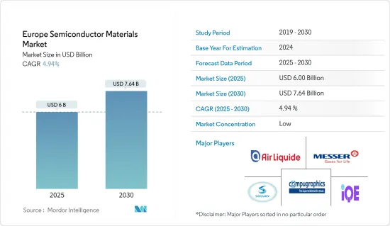
欧州の半導体材料市場規模は2025年に60億米ドルと推定され、予測期間(2025~2030年)のCAGRは4.94%で、2030年には76億4,000万米ドルに達すると予測されています。
半導体材料は、エレクトロニクス産業における重要な技術革新のひとつです。シリコン(Si)、ゲルマニウム(Ge)、ガリウムヒ素(GaAs)などの材料を採用することで、電子機器メーカーは、電子製品を重く、携帯できないものにしていた従来の熱デバイスに取って代わることができるようになりました。
主要ハイライト
- シリコンは、現在の市場シナリオで最も普及している半導体素子です。しかし、これまで以上に小型で高速な集積回路への需要が高まっているため、シリコンの効率は限界に達しており、多くの産業専門家はシリコンがまもなくムーアの法則の限界に達するのではないかと懸念しています。その一方で、新材料を開発するためのさまざまな研究イニシアチブが実施され、研究市場の技術革新を促進しています。
- さらに、半導体産業では微細化の動きが加速しており、先進ノードIC、ヘテロジニアス集積、3Dメモリーアーキテクチャの製造にはより多くの処理プロセスが必要となるため、ウエハー製造や包装材料の消費量も増加し、半導体材料の需要も拡大すると予想されます。
- エネルギー効率の向上と、それに伴うあらゆる電子機器動作における損失の低減は、産業の一般的な動向です。そのため、エネルギー効率の高い部品に対する需要は、特に電気自動車の駆動装置から充電ステーションや電源に至るまで、エネルギー集約型の用途において力強く成長すると予想されます。
- 半導体産業は最も複雑な産業のひとつと考えられています。これは、その製造に複数の加工プロセスや様々な製品が関わっていること、また、不安定な電子市場や予測不可能な需要など、厳しい環境に直面しているためです。
- 欧州を含む世界のCOVID-19パンデミックの発生は、調査対象市場のサプライチェーンと生産を大きく混乱させました。同市場の多くのエンドユーザー産業もパンデミックの影響を受け、ひいては市場に悪影響を及ぼしました。
欧州の半導体材料市場動向
半導体材料の技術進歩と製品革新
- 半導体は、新しい材料や製造方法の発見により、薄いディスクやウエハーに切断または形成されたリジッド基板から、より軟質なプラスチック材料や紙へと移行しつつあります。より軟質な基板への動向は、発光ダイオードから太陽電池やトランジスタに至るまで、数多くのデバイスを生み出しています。
- さらに2022年12月には、チップ製造への新たなアプローチを開発する英国の新興企業、プラグマティックセミコンダクタ社が投資家から3,500万米ドルを調達しました。同社はチップ製造施設(ファブ)を運営しており、壊れることなく曲がる軟質プロセッサを製造しています。最も注目すべき点は、このプロセッサにはシリコンが含まれていないことです。2022年、プラグマティック社とアーム社は、プラスチック基板上に実装された金属酸化物トランジスタで構成される軟質プロセッサPlasticArmのデモを行りました。
- ムーアの法則は、小型化、高速化、低価格化が進むコンピューターデバイスの進歩を促してきました。そのため、半導体産業は、かつて数ミクロン用に開発されたプロセスを、数ナノメートルの接合形成にいかに移行させるかという課題に取り組む必要があります。
- 欧州連合(EU)が資金を提供するプロジェクトFACIT(新技術の統合のための化合物半導体の高速アニール)において、科学者たちはIII-V族材料であるインジウム、ガリウム、ヒ素(InGaAs)をシリコンゲルマニウム(SiGe)技術と組み合わせ、CMOSチップを作ることに成功しました。新たに開発されたプロセスは、チップの大量生産に対応しており、チップメーカーにとって現実的な選択肢となります。プロジェクトチームは、同じ350~400mmの大型Siウエハーを使って、InGaAs、SiGe、SiのCMOS層を統合できるプロセスを開発しました。科学者たちはこの方法を、CMOS技術をナノメートルレベルでさらに縮小・微細化する方法として考えています。
成長を確認するコンシューマーエレクトロニクス
- 半導体材料の開発は、エレクトロニクス産業における最も重要な技術的進歩のひとつです。電子移動度が高く、動作温度範囲が広く、必要エネルギーが低いため、この材料は好まれています。半導体は大半の民生用電子機器製品に使われています。携帯電話、コンピューター、ゲーム機、電子レンジ、冷蔵庫はすべて、集積回路、ダイオード、トランジスタなどの半導体部品を採用しています。
- パワーエレクトロニクスは、システム効率に直接影響する半導体材料を使用しています。パワーエレクトロニクスシステムは、携帯電話や民生用電子機器製品に使用され、電力をある形態からによる形態に変換し、そのエネルギーレベルを調整します。そのひとつが炭化ケイ素(SiC)です。SiCは、りわけ高温・高電位での動作を可能にする特性を持っており、部品の小型化と電力変換効率の向上をもたらします。したがって、このセグメントの進歩は、SiCのような材料の必要性を直ちに高めています。
- バッテリーの寿命を延ばすという電子機器メーカーの要求が、SiC材料半導体の需要を押し上げています。消費者向けガジェットのメーカーは、自社製品のバッテリーをアップグレードしています。このセグメントの市場拡大は、低充電ガジェットに対する消費者の欲求が原動力となっています。この市場におけるSiC半導体の主要消費者は、スマートフォン、ウェアラブル機器、その他の主要民生用電子機器製品のメーカーです。
- メーカーや政府は、比較的短時間でデバイスを充電できるスマートフォン用充電器を開発しています。そのため、これらの定格電流は0.5ミリアンペアから5ミリアンペアに増加しています。USB-Cとオンボード・アダプターのSiC半導体は、必要な電流と電圧レベルを維持するために不可欠です。ウェアラブルデバイス市場とPC市場は、どちらも同様の軌跡をたどっています。将来世代のオンボード充電器とUSB-CアダプターのGaNand SiCデバイスは、超高電力密度を記載しています。OPPO、One Plus、Motorola、Samsung、Appleなどのメーカーによるこれらの急速充電アダプターの配布は、マーケティング戦術の要となっています。
欧州の半導体材料産業概要
欧州の半導体材料市場は適度な競争があり、複数の大手企業で構成されています。市場は適度に集中しているように見えます。新規参入には高い障壁があります。新規参入者は高い資本要件に満足しなければならず、一方、技術集約的な市場の性質上、市場開拓者は技術開発を綿密に追跡することが不可欠です。
- 2022年10月-IQE(International Quantum Epitaxy)PLCはSKシリコンと化合物半導体製品の開発・商業化に向けた戦略的提携契約を締結。IQEとSKウルトロンは、無線通信市場における無線周波数向けのSiC(炭化ケイ素)上のGaN(窒化ガリウム)と、様々な市場におけるパワーエレクトロニクス向けのSi(シリコン)上のGaNをベースとした革新的なエピウエハーの開発と提供に注力します。
- 2022年7月-BASFと戸田工業株式会社(TODA)は、日本の小野田事業所におけるBASF TODA Battery Materials LLC(BTBM)の生産能力をさらに拡大すると発表しました。この拡大により、年間最大45GWhのセル容量に対応する高ニッケル正極活物質の供給が増加します。この拡大は、産業と消費者産業にわたる二次電池と合金の製造において、半導体メーカーへの利益を増大させています。
その他の特典
- エクセル形式の市場予測(ME)シート
- 3ヶ月間のアナリストサポート
目次
第1章 イントロダクション
- 調査の前提条件と市場定義
- 調査範囲
第2章 調査手法
第3章 エグゼクティブサマリー
第4章 市場洞察
- 市場概要
- 産業の魅力-ポーターのファイブフォース分析
- 供給企業の交渉力
- 消費者の交渉力
- 新規参入業者の脅威
- 代替品の脅威
- 競争企業間の敵対関係の強さ
- 産業バリューチェーン/サプライチェーン分析
- COVID-19の市場への影響
第5章 市場力学
- 市場の促進要因
- 半導体材料の技術進歩と製品革新
- 民生用電子機器製品の需要増加
- OSAT/包装企業からの需要増加
- 市場抑制要因
- 製造プロセスの複雑さ
第6章 市場セグメンテーション
- 用途別
- ファブリケーション
- プロセス化学
- フォトマスク
- 電子ガス
- フォトレジスト
- スパッタリング対象
- シリコン
- その他の製造用途
- 包装
- 基板
- リードフレーム
- セラミック包装
- ボンディングワイヤ
- 封止樹脂(液状)
- ダイアタッチ材料
- その他の包装用途
- ファブリケーション
- エンドユーザー産業別
- コンシューマーエレクトロニクス
- 通信産業
- 製造業
- 自動車
- エネルギー公益事業
- その他
第7章 競合情勢
- 企業プロファイル
- Solvay SA
- Messer SE & Co. KGaA
- Air Liquide SA
- Compugraphics(MacDermid Alpha Electronics Solutions)
- International Quantum Epitaxy PLC(IQE PLC)
- BASF SE
- Henkel AG & Co. KGaA
- Caplinq Europe BV
第8章 市場展望
The Europe Semiconductor Materials Market size is estimated at USD 6.00 billion in 2025, and is expected to reach USD 7.64 billion by 2030, at a CAGR of 4.94% during the forecast period (2025-2030).
Semiconductor materials represent one of the significant innovations in the electronics industry. By employing materials such as silicon (Si), germanium (Ge), and gallium arsenide (GaAs), electronics manufacturers have been able to replace traditional thermal devices that made electronic items heavy and non-portable.
Key Highlights
- Silicon is the most popular semiconductor element available in the current market scenario. However, the increasing demand for ever-smaller, faster-integrated circuits has pushed the efficiency of the material to its limits, with many industry experts fearing silicon will soon reach the limits of Moore's Law. In the meantime, various research initiatives are being undertaken to develop new materials, driving innovation in the studied market.
- Moreover, with the miniaturization trend gaining momentum in the semiconductor industry, the demand for semiconductor materials is also expected to grow as manufacturing advanced node ICs, heterogeneous integration, and 3D memory architectures require more processing steps, driving higher wafer fabrication and packaging materials consumption as a result.
- Higher energy efficiency and resulting lower losses in all electronic operations is a general trend in the industry. As such, the demand for energy-efficient components is expected to grow strongly, especially in energy-intensive applications, from electric vehicle drives to charging stations and power supplies.
- The semiconductor industry is considered one of the most complex industries. This is because more than several processing steps and various products are involved in their manufacturing and the harsh environment it faces, e.g., the volatile electronic market and the unpredictable demand.
- The outbreak of the COVID-19 pandemic worldwide, including in Europe, significantly disrupted the supply chain and production of the market studied. Many end-user industries of the market were also affected by the pandemic, which, in turn, had a negative impact on the market.
Europe Semiconductor Materials Market Trends
Technical Advancement and Product Innovation of the Semiconductor Materials
- Semiconductors are moving away from rigid substrates, cut or formed into thin discs or wafers, to more flexible plastic material and paper, all due to new material and fabrication discoveries. The trend toward more flexible substrates has led to numerous devices, from light-emitting diodes to solar cells and transistors.
- Moreover, in December 2022, Pragmatic Semiconductor Ltd, a UK-based startup developing a new approach to chip production, raised USD 35 million from investors. The company operates a chip fabrication facility, or fab, that manufactures flexible processors that bend without breaking. Most notably, the processors do not contain silicon. In 2022, Pragmatic and Arm Ltd demonstrated a flexible processor, PlasticArm, which consists of metal-oxide transistors implemented on a plastic substrate.
- Moore's law has been driving advances in computing devices as they keep getting smaller, faster, and cheaper. Thus, the semiconductor industry needs to address the challenge of how to migrate processes that were once developed for a few microns to be able to form junctions that are a few nanometers in scale.
- Within the project FACIT (fast annealing of compound semiconductors for integration of new technologies), which is funded by the European Union, scientists have successfully combined III-V materials, indium, gallium, and arsenide (InGaAs), with silicon germanium (SiGe) technology to create CMOS chips. The newly developed process is compatible with high-volume chip fabrication, which makes it a viable option for chip manufacturers. Using the same large-sized Si wafer of 350-400 mm, the project team has developed a process that allows the integration of InGaAs, SiGeand Si CMOS layers. Scientists have considered this method as a way of further shrinking and scaling CMOS technology at a nanometer level.
Consumer Electronics to Witness the Growth
- The creation of semiconductor materials is one of the most significant technological advances in the electronics industry. Because of its high electron mobility, wide operating temperature range, and low energy need, the material is well-liked. Semiconductors are used in the majority of consumer electronics. Mobile phones, computers, game consoles, microwaves, and refrigerators all employ semiconductor components, including integrated circuits, diodes, and transistors.
- Power electronics use semiconductor materials, which directly impact system efficiency. Power electronics systems are used by mobile phones and home appliances to convert electrical power from one form to another and regulate its energy level. One of these is silicon carbide (SiC), which has characteristics that, among other things, enable operation at higher temperatures and higher electrical potential, resulting in smaller components and greater power conversion efficiency. Thus, advancements in this area immediately raise the need for materials like SiC.
- The requirement for electronic makers to extend battery life is fuelling the demand for SiCmaterial semiconductors. Manufacturers of consumer gadgets are upgrading the batteries in their products. The market expansion of this sector is driven by consumer desire for low-charging gadgets. The primary consumers of SiC semiconductors in this market are the manufacturers of smartphones, wearable devices, and other major consumer electronics.
- Manufacturers and governments are creating smartphone chargers that can charge the device in a relatively short period. Therefore, the current rating for these has increased from 0.5 milliamps to 5 milliamps. The USB-C and On Board adapters' SiC semiconductors are essential for sustaining the necessary current and voltage levels. The wearable device and PC markets have both followed a similar trajectory. GaNand SiC Devices in the future generation of onboard chargers and USB-C adapters provide ultra-high power density. The distribution of these fast-charging adapters by producers like OPPO, One Plus, Motorola, Samsung, and Apple is the cornerstone of their marketing tactics.
Europe Semiconductor Materials Industry Overview
The European semiconductor materials market is reasonably competitive and consists of several major players. The market appears to be moderately concentrated. The market poses high barriers to entry for new firms. New entrants must be content with high capital requirements, while the technology-intensive nature of the market makes it imperative for market players to closely track technological developments.
- October 2022 - IQE (International Quantum Epitaxy) PLC entered into a strategic collaboration agreement with SK silicon to develop and commercialize compound semiconductor products. IQE and SK Ultron will focus on developing and delivering innovative epi wafers based upon GaN (Gallium Nitride) on SiC (Silicon Carbide) for radio frequency applications in the wireless communications market and GaN on Silicon (Si) for power electronics applications across various markets.
- July 2022 - BASF and Toda Kogyo Corp. (TODA) announced that they would further expand the production capacity of BASF TODA Battery Materials LLC (BTBM) at the Onoda site in Japan. This expansion increases the supply of high nickel cathode active materials for up to 45 GWh cell capacity per year. This expansion would increase benefits for the semiconductor manufacturers in manufacturing rechargeable batteries and alloys across industrial and consumer industries.
Additional Benefits:
- The market estimate (ME) sheet in Excel format
- 3 months of analyst support
TABLE OF CONTENTS
1 INTRODUCTION
- 1.1 Study Assumptions and Market Definition
- 1.2 Scope of the Study
2 RESEARCH METHODOLOGY
3 EXECUTIVE SUMMARY
4 MARKET INSIGHTS
- 4.1 Market Overview
- 4.2 Industry Attractiveness - Porter's Five Forces Analysis
- 4.2.1 Bargaining Power of Suppliers
- 4.2.2 Bargaining Power of Consumers
- 4.2.3 Threat of New Entrants
- 4.2.4 Threat of Substitute Products
- 4.2.5 Intensity of Competitive Rivalry
- 4.3 Industry Value Chain/Supply Chain Analysis
- 4.4 Impact of COVID-19 on the Market
5 MARKET DYNAMICS
- 5.1 Market Drivers
- 5.1.1 Technical Advancement and Product Innovation of the Semiconductor Materials
- 5.1.2 Rising Demand for Consumer Electronics Goods
- 5.1.3 Increased Demand from OSAT/Packaging Companies
- 5.2 Market Restraints
- 5.2.1 Complexity in the Manufacturing Process
6 MARKET SEGMENTATION
- 6.1 By Application
- 6.1.1 Fabrication
- 6.1.1.1 Process Chemicals
- 6.1.1.2 Photomasks
- 6.1.1.3 Electronic Gases
- 6.1.1.4 Photoresists Ancillaries
- 6.1.1.5 Sputtering Targets
- 6.1.1.6 Silicon
- 6.1.1.7 Other Fabrication Applications
- 6.1.2 Packaging
- 6.1.2.1 Substrates
- 6.1.2.2 Lead Frames
- 6.1.2.3 Ceramic Packages
- 6.1.2.4 Bonding Wire
- 6.1.2.5 Encapsulation Resins (Liquid)
- 6.1.2.6 Die Attach Materials
- 6.1.2.7 Other Packaging Applications
- 6.1.1 Fabrication
- 6.2 By End-user Industry
- 6.2.1 Consumer Electronics
- 6.2.2 Telecommunication
- 6.2.3 Manufacturing
- 6.2.4 Automotive
- 6.2.5 Energy and Utility
- 6.2.6 Other End-User Industries
7 COMPETITIVE LANDSCAPE
- 7.1 Company Profiles
- 7.1.1 Solvay SA
- 7.1.2 Messer SE & Co. KGaA
- 7.1.3 Air Liquide SA
- 7.1.4 Compugraphics (MacDermid Alpha Electronics Solutions)
- 7.1.5 International Quantum Epitaxy PLC (IQE PLC)
- 7.1.6 BASF SE
- 7.1.7 Henkel AG & Co. KGaA
- 7.1.8 Caplinq Europe BV
