
|
市場調査レポート
商品コード
1630292
組み込み型ダイパッケージング-市場シェア分析、産業動向と統計、成長予測(2025年~2030年)Embedded Die Packaging - Market Share Analysis, Industry Trends & Statistics, Growth Forecasts (2025 - 2030) |
||||||
カスタマイズ可能
適宜更新あり
|
|||||||
| 組み込み型ダイパッケージング-市場シェア分析、産業動向と統計、成長予測(2025年~2030年) |
|
出版日: 2025年01月05日
発行: Mordor Intelligence
ページ情報: 英文 132 Pages
納期: 2~3営業日
|

全表示
- 概要
- 目次
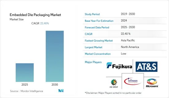
組み込み型ダイパッケージング市場は予測期間中にCAGR 22.4%を記録する見込み
主要ハイライト
- 製品の小型化・多機能化が進み、デバイスの小型化が市場を牽引マイクロマシニングとナノ技術は、生物医療用途から化学マイクロリアクターやセンサーに至るまで、部品の小型化においてますます重要な役割を果たしています。例えば、Bluetooth無線LANモジュールは、今日の高密度携帯機器では最小限の回路基板面積しか必要としないです。
- 電気的・熱的性能の向上が市場を牽引しています。パワーマネージメントやモバイルワイヤレス用途では、薄型化だけでなく優れた熱性能により、組込み技術がアセンブリ製造に取って代わるものと評価されています。組み込みダイの熱性能は、銅クリップを使用したPQFNよりも約17%優れています。また、電気自動車向けに、埋め込みダイと再配線層(RDL)技術を使用して、電気的性能と熱的性能を向上させるパワーデバイス用の新しい拡大可能な先進パッケージングを開発しました。
- さらに、高周波での優れた電気的性能により、この技術は新興のIT・通信用途の有望な技術としても認識されています。通信用途へのこの技術の展開を助けるさまざまな利点には、電子回路の機能性と効率の向上、電力と信号のインダクタンス、信頼性の向上、信号密度の向上などがあります。
- テスト、検査、手直しが困難な組込みダイ技術は、市場成長の課題です。フィーチャ(ラインやスペース)が2μm以下に微細化すると、欠陥を見ることが難しくなります。さらに、用途によってはビアホール内の破片を見つけることが懸念されるようになります。
- COVID-19の発生以来、エレクトロニクス産業は大きな打撃を受け、サプライチェーンや生産設備に大きな影響を及ぼしています。2月から3月にかけて中国と台湾で生産が停止し、世界中の様々なOEMに影響を与えました。
組み込み型ダイパッケージング市場動向
軟質基板のダイが大きな市場シェアを占める見込み
- 技術の進歩に伴い、プリント基板の製品販売額は増加しており、様々なウェアラブルデバイスやIoTデバイスに軟質基板が採用されるようになったことで、売上は今後さらに伸びると予想されます。
- ストレッチャブル・エレクトロニクス(SC)は今のところ商業的なもので、様々な形や形態があります。この技術では、主に軟質基板と呼ばれる標準的なプリント基板を使用し、液体射出成形技術によってエラストマーを組み込んだ伸縮可能な電子回路を形成することで、堅牢で信頼性の高い製品を実現しています。例えば、軍事用途では、制服や鎧に柔軟で軽量な衝撃センサーを埋め込むことができ、戦闘中に受けた傷害の情報を保存し、より良い情報を提供することができます。
- 軟質ハイブリッド・エレクトロニクス(FHE)は、電子回路製造の新しいアプローチと考えられており、従来のエレクトロニクスとプリンテッドエレクトロニクスの長所を組み合わせることを目指しています。ICはフォトリソグラフィで製造され、ベアダイとして実装されます。
- 軟質回路の組み込み活動は、様々な小型電子機器への実装のために高い傾向にあります。例えば、2019年9月、IDEMIAとZwipeは生体認証決済カードソリューションのために協業し、セキュア・エレメントやマイクロコントローラのようなものがすべて軟質プリント回路基板に実装されたシングルチップに組み込まれており、比較的少ない部品点数で差別化される予定です。
- さらに、スポーツ・用途や医療向けの自律システムは、微細な構造が最大の柔軟性と快適性をもたらすため、主に小さなフォーム・ファクターの恩恵を受ける。市販のICを軟質回路基板(FCB)に組み込むことで、システム全体のサイズを小さくすることができます。液晶ポリマー(LCP)をセンサーの基材として使用することは、医療用製品で非常に多く使用されています。医療用途の小型化されたスマートセンサ・モジュールは、従来のフレックス回路薄膜や標準的な組立プロセスや装置を使用して、LCP基板から製造することができます。
北米が大きな市場シェアを占める見込み
- 米国はまた、19の州にまたがる80のウエハー製造工場を擁する半導体パッケージング技術革新のフロントランナーであり、組み込みダイによる小型化などの新技術が導入されています。これとは別に、世界企業による米国への投資が市場を活性化させています。
- 例えば、Intelは、組み込み型マルチダイ・インターコネクト・ブリッジ(EMIB)を通じて、Intelの3Dシステムインパッケージング技術を利用した次世代プラットフォームを実現しようとしています。産業では、この用途を2.5Dパッケージング統合と呼んでいます。EMIB(Embedded Multi-die Interconnect Bridge)は、他の2.5Dアプローチで一般的な大型のシリコンインターポーザーを使用する代わりに、複数の配線層を持つ非常に小さなブリッジダイを使用します。このブリッジ・ダイは、当社の基板製造プロセスの一部として組み込まれています。
- これとは別に、米国には、電気自動車セグメントに投資している世界の大手自動車メーカーがあります。組込みシステムは、アダプティブクルーズコントロールのような運転支援機能によって運転の快適性を高めます。また、大幅な省エネを達成するためには、車両全体の電源管理を制御する分散型組込み制御アプローチが必要になります。これにより、組込みダイ技術の需要が増加することになります。
組み込み型ダイパッケージング産業概要
組込みダイパッケージング市場は、自動車、産業、民生用電子機器のエンドユーザーが増加しているため、細分化されています。市場の既存参入企業は、5G通信、高性能データセンター、小型電子機器などの新技術に対応することで競合を維持しようとしています。主要参入企業は、Microsemi Corporation、Fujikura Ltdなどです。最近の市場開拓の動向は以下の通り。
- 2020年10月-米国国防総省はIntel Federal LLCにヘテロジニアス・インテグレーション・プロトタイプ(SHIP)プログラムの第2フェーズを授与しました。SHIPプログラムにより、米国政府はアリゾナ州とオレゴン州にあるIntelの最先端半導体パッケージング能力を利用し、Intelの年間数百億米ドルの研究開発と製造投資によって生み出された能力を活用することができます。このプロジェクトは、Naval Surface Warfare Centre, Crane Divisionが実行し、National Security Technology Acceleratorが管理します。
- 2019年9月-FPGAベースのハードウェア・アクセラレータデバイスと高性能eFPGA IPの大手サプライヤーであるAchronix Semiconductor Corporationは、TSMCオープン・イノベーションプラットフォーム(OIP)の主要コンポーネントであるTSMC IPアライアンス・プログラムに参加しました。Achronixは、TSMC Open Innovation Platform Ecosystem Forumのブースで、同社のSpeedcore IPが顧客の用途ごとに独自のサイズで最適化されていることを実演しました。
その他の特典
- エクセル形式の市場予測(ME)シート
- 3ヶ月間のアナリストサポート
目次
第1章 イントロダクション
- 調査の前提条件と市場定義
- 調査範囲
第2章 調査手法
第3章 エグゼクティブサマリー
第4章 市場力学
- 市場概要
- 市場促進要因
- デバイスの小型化の進展
- 電気的・熱的性能の向上
- 市場抑制要因
- 検査、テスト、リワークの難しさ
- バリューチェーン分析
- 産業の魅力-ポーターのファイブフォース分析
- 供給企業の交渉力
- 買い手/消費者の交渉力
- 新規参入業者の脅威
- 代替品の脅威
- 競争企業間の敵対関係の強さ
- COVID-19の市場への影響
第5章 技術スナップショット
- PCBの小型化
- 先進的組み込みアクティブシステムインテグレーション
第6章 市場セグメンテーション
- プラットフォーム
- リジッド基板のダイ
- 軟質基板ダイ
- ICパッケージング基板
- エンドユーザー
- コンシューマー・エレクトロニクス
- IT・通信
- 自動車
- 医療
- その他
- 地域
- 南北アメリカ
- 欧州・中東・アフリカ
- アジア太平洋
第7章 競合情勢
- 企業プロファイル
- Microsemi Corporation
- Fujikura Ltd
- Infineon Technologies AG
- ASE Group
- AT&S Company
- Schweizer Electronic AG
- Intel Corporation
- Taiwan Semiconductor Manufacturing Company
- Shinko Electric Industries Co. Ltd
- Amkor Technology
- TDK Corporation
第8章 投資分析
第9章 市場機会と今後の動向
The Embedded Die Packaging Market is expected to register a CAGR of 22.4% during the forecast period.
Key Highlights
- Growing miniaturization of devices is driving the market as products are becoming increasingly smaller and embed more functionality. Micromachining and nanotechnology play an increasingly important role in the miniaturization of components ranging from biomedical applications to chemical microreactors and sensors. For instance, Bluetooth wifi modules requires minimal circuit board area on today's high-density mobile devices.
- Improved electrical & thermal performance is driving the market. For power management and mobile-wireless application the embedded technology has been evaluated to replace assembles fabrication by not only thinner thickness but due to superior thermal performance. The thermal performance of embedded die is better than PQFN with copper clip about 17%. Also a new and expandable advanced package for power devices is developed using embedded dies and redistribution layer (RDL) technology for electric car to improve the electric and thermal performance.
- Further, owing to its excellent electrical performance at high frequencies, the technology is also being perceived as a promising technology for emerging telecommunication applications. Various advantages that aid the deployment of the technology in telecommunication applications include increased functionality and efficiency of the electronic circuits, power and signal inductance, improved reliability, and higher signal density.
- Difficulty to test, inspect and rework, the embedded die technology challenges the market to grow. As features (lines and spaces) shrink to 2µm and below, it becomes more difficult to see defects. In addition, finding debris in via holes becomes a concern in some applications.
- Since the outbreak of COVID-19, the electronics industry has been hit severely, with a significant influence on its supply chain and production facilities. The production came to a stand still in China and Taiwan during February and March, which influenced various OEMs across the world.
Embedded Die Packaging Market Trends
Die in Flexible Board Expected to Hold Significant Market Share
- With the increased advancement in technology, the product sale value of the printed circuit board is increasing and with the increased adoption of the flexible board in various wearable and IoT devices, the sales are expected to grow higher in future.
- Stretchable Electronics (SC) is so far commercial and comes in many shapes and forms. The technology uses standard printed circuit board, mainly flexible board, where liquid injection molding techniques involve elastomer embedded stretchable electronic circuit, which achieves a robust and reliable product. For instance, in military usage, uniforms and armors can have embedded, flexible, lightweight impact sensors that could store and provide better information of the injury sustained during combat.
- Flexible hybrid electronics (FHE), which is considered as a novel approach to electronic circuit manufacturing, aims to combine the best of conventional and printed electronics. Additional components and as many as conductive interconnects are possible to be printed onto a flexible substrate, whereas the IC is produced using photolithography and then mounted, as a bare die.
- The embedding activity of flexible circuits are in high trend for their implementation in various miniature electronic devices. For instance, in September 2019, IDEMIA and Zwipe collaborated for a biometric payment card solution, where the solution is planned to be distinguished by its relatively small number of components, with things, like the Secure Element and the microcontroller, all embedded in a single chip mounted on a flexible printed circuit board.
- Further, autonomous systems for sports applications and healthcare mainly benefit from a small form factor, as minute structures result in maximal flexibility and comfort. The embedding of a commercially available IC in a flexible circuit board (FCB) can reduce the overall size of a system. The usage of liquid crystal polymer (LCP) as base material for sensors are highly used in medical products. Miniaturized smart sensor modules for medical applications can be fabricated from LCP substrates using conventional flex circuit thin film and standard assembly processes and equipment.
North America Expected to Hold Significant Market Share
- Countries in the region, such as United States assist the world in manufacturing, designing, and researching related to the semiconductor industry and United States is also the frontrunner in semiconductor packaging innovation having 80 wafer fabrication plants spread across 19 states where new technologies is being implemented such as miniaturization through embedded die etc. Apart from this, investments in this country by global players are setting to fuel the market.
- For instance, Intel is enabling Next-Generation Platforms using Intel's 3D System-in-package technology through Embedded Multi-die Interconnect Bridge (EMIB) , an elegant and cost-effective approach to in-package high density interconnect of heterogeneous chips. The industry refers to this application as 2.5D package integration. Instead of using a large silicon interposer typically found in other 2.5D approaches, Embedded Multi-die Interconnect Bridge (EMIB) uses a very small bridge die, with multiple routing layers. This bridge die is embedded as part of our substrate fabrication process.
- Apart from this, the United States is home to some of the major automotive players in the world, which are investing in the electric car segment. The embedded systems increases the driving comfort with driver assistance functions like adaptive cruise control. Also to achieve significant energy savings, a distributed embedded control approach becomes necessary to control the power management of the entire vehicle. This is set to increase the demand for embedded die technology.
Embedded Die Packaging Industry Overview
The embedded die packaging market is fragmented due to the growing number of end-users in automotive, industrial, and consumer electronics. The existing players in the market are striving to maintain a competitive edge by catering to newer technologies, such as 5G telecommunication, high-performance data centers, compact electronic devices, etc. Key players are Microsemi Corporation, Fujikura Ltd, etc. Recent developments in the market are -
- October 2020 - The U.S. Department of Defence awarded Intel Federal LLC the second phase of its Heterogeneous Integration Prototype (SHIP) program. The SHIP program enables the US government to access Intel's state-of-the-art semiconductor packaging capabilities in Arizona and Oregon and take advantage of capabilities created by Intel's tens of billions of dollars of annual R&D and manufacturing investment. The project is executed by the Naval Surface Warfare Centre, Crane Division, and administered by the National Security Technology Accelerator.
- Sep 2019 - Achronix Semiconductor Corporation, a leading supplier in FPGA-based hardware accelerator devices and high-performance eFPGA IP, joined the TSMC IP Alliance Program, a key component of TSMC Open Innovation Platform (OIP). Achronix demonstrated how its Speedcore IP is uniquely sized and optimized for each customer's application in its booth at TSMC Open Innovation Platform Ecosystem Forum.
Additional Benefits:
- The market estimate (ME) sheet in Excel format
- 3 months of analyst support
TABLE OF CONTENTS
1 INTRODUCTION
- 1.1 Study Assumptions and Market Definition
- 1.2 Scope of the Study
2 RESEARCH METHODOLOGY
3 EXECUTIVE SUMMARY
4 MARKET DYNAMICS
- 4.1 Market Overview
- 4.2 Market Drivers
- 4.2.1 Growing Miniaturization of Devices
- 4.2.2 Improved Electrical and Thermal Performance
- 4.3 Market Restraints
- 4.3.1 Difficulty to Inspect, Test and Rework
- 4.4 Industry Value Chain Analysis
- 4.5 Industry Attractiveness - Porter's Five Forces Analysis
- 4.5.1 Bargaining Power of Suppliers
- 4.5.2 Bargaining Power of Buyers/Consumers
- 4.5.3 Threat of New Entrants
- 4.5.4 Threat of Substitute Products
- 4.5.5 Intensity of Competitive Rivalry
- 4.6 Impact of COVID-19 on the Market
5 TECHNOLOGY SNAPSHOT
- 5.1 PCB Miniaturization
- 5.2 Advanced Embedded Active System Integration
6 MARKET SEGMENTATION
- 6.1 Platform
- 6.1.1 Die in Rigid Board
- 6.1.2 Die in Flexible Board
- 6.1.3 IC Package Substrate
- 6.2 End User
- 6.2.1 Consumer Electronics
- 6.2.2 IT and Telecommunications
- 6.2.3 Automotive
- 6.2.4 Healthcare
- 6.2.5 Other End Users
- 6.3 Geography
- 6.3.1 Americas
- 6.3.2 Europe and MEA
- 6.3.3 Asia-Pacific
7 COMPETITIVE LANDSCAPE
- 7.1 Company Profiles
- 7.1.1 Microsemi Corporation
- 7.1.2 Fujikura Ltd
- 7.1.3 Infineon Technologies AG
- 7.1.4 ASE Group
- 7.1.5 AT&S Company
- 7.1.6 Schweizer Electronic AG
- 7.1.7 Intel Corporation
- 7.1.8 Taiwan Semiconductor Manufacturing Company
- 7.1.9 Shinko Electric Industries Co. Ltd
- 7.1.10 Amkor Technology
- 7.1.11 TDK Corporation
