
|
市場調査レポート
商品コード
1690962
半導体バックエンド装置:市場シェア分析、産業動向・統計、成長予測(2025年~2030年)Semiconductor Back-End Equipment - Market Share Analysis, Industry Trends & Statistics, Growth Forecasts (2025 - 2030) |
||||||
カスタマイズ可能
適宜更新あり
|
|||||||
| 半導体バックエンド装置:市場シェア分析、産業動向・統計、成長予測(2025年~2030年) |
|
出版日: 2025年03月18日
発行: Mordor Intelligence
ページ情報: 英文 137 Pages
納期: 2~3営業日
|

全表示
- 概要
- 目次
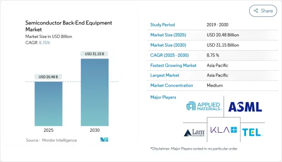
半導体バックエンド装置の市場規模は2025年に204億8,000万米ドル、2030年には311億5,000万米ドルに達すると予測、予測期間(2025-2030年)のCAGRは8.75%。
主なハイライト
- エネルギー転換、電動化、AIなどの技術を取り入れることが、世界市場における半導体需要を再形成する最前線となっています。例えば、人工知能(AI)を半導体産業に組み込むことは、革新、効率、機会の新時代を告げるものです。過去において、半導体産業は主に他のハイテク分野のイネーブラーとして機能していました。
- しかし、AIによって、半導体は技術開発を変革する最前線に立ち、業界の経済情勢を再構築しています。例えば、AIを搭載したチップは自動運転車に使われています。これにより、周囲の状況に基づいてリアルタイムで判断することが可能になります。また、AIを搭載したチップはヘルスケア業界でも患者のリアルタイム監視や健康問題の検出に使われています。こうしたイノベーションは、生活や働き方を一変させ、生活をより身近で効率的なものにします。
- さらに、再生不可能な燃料への依存を減らし、気候変動と闘うために、世界はますます再生可能エネルギー源へとシフトしています。電化はこの移行を達成するための重要な戦略であり、半導体はエネルギーの生成、貯蔵、消費の方法を変革する上で中心的な役割を果たしています。
- 半導体、特にアナログ製品や組込みプロセッシング製品は、よりスマートで信頼性が高く、利用しやすい太陽エネルギー貯蔵システムや電気自動車充電システムを通じて電化を実現するのに適した位置にあります。このように、各企業は、高電圧パワー、電流・電圧センシング、エッジ・プロセッシング、コネクティビティ製品の4つの重要分野に注力することで、様々なエンドユーザー市場における半導体の力学の変化に対応し、先進半導体ウエハー、パッケージング、組立工程の後工程装置の役割を推進するという重要な役割を果たしています。
- 半導体産業は急速に拡大しており、半導体製造装置の需要も急増しています。しかし、半導体製造装置の価格は半導体産業にとって非常に重要な要素となっています。装置コストは半導体の生産コストに顕著な影響を及ぼし、最終製品の価格に影響を与えます。これが市場の成長を抑制すると予想されます。
- マクロ経済の不確実性、個人消費の減少、世界経済の変動といった要因は、チップ需要を阻害すると予想されます。一般的に、景気後退期には個人消費が減少し、半導体に大きく依存するスマートフォン、タブレット、ノートパソコンなどの家電製品の需要が減少します。仮に世界経済の悪化が続き、消費者需要がさらに弱まるとしよう。その場合、これらの要因は今後数年間、半導体市場に悪影響を及ぼすと予想されます。
半導体バックエンド装置市場の動向
アセンブリ・パッケージングセグメントが大幅な成長を遂げる見込み
- このセグメントの成長は、ファンアウト・ウェーハレベル・パッケージング(FOWLP)、ウェーハレベル・パッケージング(WLP)、システム・イン・パッケージ(SiP)といった最先端のパッケージング技術が受け入れられつつあることが背景にあるとみられます。さらに、最近の先進パッケージングにより、複数の集積回路を単一パッケージに統合できるスタックドWLCSPのようなパッケージング技術も登場しています。これらの進歩は、ロジックチップとメモリーチップの組み合わせや、積層メモリーチップを包含しています。その結果、先進パッケージングの需要は急増すると予想され、それに対応する装置の購入が必要となります。
- 様々な分野での半導体ICの利用の急増は、半導体パッケージングとアセンブリ装置への要求の上昇につながっています。その一例として、エレクトロニクス業界では、電子機器とそのアプリケーションの普及により、こうした装置の必要性が拡大しています。これが需要増に大きく寄与していると予想されます。同様に、半導体の小型化、高速化、高効率化に対するニーズの高まりが、先進パッケージング技術に対する需要を後押しし、半導体パッケージング装置の需要を高めています。
- さまざまな産業における半導体の世界のニーズの高まりは、半導体の生産能力の拡大につながり、結果として半導体バックエンド装置市場の成長を後押ししています。2023年8月、著名な半導体鋳造工場であるTSMCは、最先端のパッケージング装置を提供する複数のサプライヤーに新規発注を開始しました。Gudeng Precision Industrial、Apic Yamada、Disco、Scientechは、同社と緊密に協力しているサプライヤーのひとつです。TSMCが装置サプライヤーとの提携を決定したのは、先進パッケージング能力の強化に向けた同社の継続的な取り組みを反映したものです。
- 半導体チップの利用と生産が著しく伸びていることは、半導体パッケージングと組立装置セクターの拡大を支える重要な原動力となっています。さらに、SIAが支援するWSTSによる最近の業界予測では、2023年の世界売上高は9.4%減少し、その後2024年には13.1%増加すると予測しています。この予測では、2023年の世界売上高は5,200億米ドルに達し、2022年の5,741億米ドルから減少すると予測しています。2024年には、世界売上高は5,884億米ドルに増加すると予想されています。こうした前向きな業界動向は、包装機器ベンダーが市場機会を活用することを可能にすると思われます。
- 同市場は、マイクロン、TSMC、ASEといった著名ベンダーがパッケージング技術に投資していることに加え、他のベンダーがこれらの技術によってもたらされる利点を活用していることによって牽引されると予想されます。アップル、サムスン、インテルなどは、先進チップパッケージング(ACP)を利用して、複数のコンポーネントを1枚の基板に統合することでデバイスの性能と効率を高めています。このような企業の採用は、ATP装置の成長を促進すると思われます。
アジア太平洋地域が市場の大幅な成長に期待
- 中国は、1,500億米ドルの資金援助を受けて、野心的な半導体アジェンダを推進しています。同国は国内IC産業を強化し、チップ生産を増加させることを目指しています。現在進行中の米国と中国の貿易戦争は、最先端のプロセス技術が集中するこの重要な分野での緊張を激化させ、多くの中国企業を半導体鋳造工場への投資に導いています。中国は、鋳造、窒化ガリウム(GaN)、炭化ケイ素(SiC)市場における大幅な拡大キャンペーンなど、半導体部門を強化するためのさまざまなイニシアチブを発表しています。
- 同地域における半導体事業の成長とチップ生産能力の向上は、後工程装置の需要を促進すると予想されます。中国のハイテク産業は、通信、再生可能エネルギー、電気自動車(EV)における強力なプレゼンスを活用することで、世界のテクノロジー・バリュー・チェーンを上昇させることを目指しています。
- これらの分野に加え、同産業は現在、先端半導体にも注力しています。この移行は主に、先進ノード製造の進歩、メモリー市場の拡大、炭化ケイ素(SiC)競争への積極的関与、先進パッケージングと製造装置への戦略的投資によって推進されています。中国全土でファウンドリー事業の拡大とファブへの投資が進み、市場が活性化すると予想されます。
- 韓国はここ数年、半導体産業で顕著な成長を遂げており、生産量と出荷量の両方が大幅に増加しています。この急成長は技術進歩の復活を示しており、韓国経済と世界のハイテクセクターにとって良い兆しです。サムスンやSKハイニックスといった韓国の主要半導体企業は、世界の半導体産業における主要企業としての地位を確立しています。この地域におけるチップ生産能力の拡大は、後工程装置市場をさらに押し上げると思われます。
- 同地域の様々な市場におけるチップ需要の急増は、後工程半導体ビジネスへの注目をもたらしています。後工程を専門とする企業は、今後数年間、積極的な投資と技術的進歩を持続すると予想されます。
半導体バックエンド装置産業の概要
半導体バックエンド装置市場は、世界プレーヤーと中小企業の両方が存在するため、半固体化しています。市場の主要企業には、ASML Holding NV、Applied Materials Inc.、LAM Research Corporation、東京エレクトロン株式会社、KLA Corporationなどがあります。市場のプレーヤーは、製品ラインナップを強化し、持続可能な競争優位性を獲得するために、パートナーシップ、事業拡大、買収などの戦略を採用しています。
- 2023年12月アプライドマテリアルズとCEA-Letiは、ICAPS市場(IoT、通信、自動車、電力、センサー)に対応する特殊半導体アプリケーション向けの材料工学ソリューションに焦点を当てた共同ラボを設立し、協力関係を拡大しました。このラボは、IoT、電気自動車、スマートグリッドインフラの需要に対応することで、次世代デバイスのイノベーションを加速することを目的としています。プロジェクトでは、ICAPSデバイスの性能向上、消費電力の削減、市場投入までの時間短縮を実現するための材料工学の課題に取り組みます。
- 2023年11月サムスン電子とASMLホールディングは、韓国における共同研究開発施設に1兆ウォン(7億6,000万米ドル)を投資する予備契約を締結。ASML本社で調印された覚書に記載されたこの提携は、ASMLの最先端極端紫外線(EUV)装置を使用したメモリーチップの開発に焦点を当てたものです。世界で唯一のEUVスキャナーメーカーであるASMLの技術は、半導体の複雑なパターニング、製造の合理化、生産歩留まりの向上に極めて重要です。研究開発センターは、ASMLが共同で設立した初の海外施設であり、次世代EUV技術に基づく超微細半導体製造プロセスの開発に集中します。
その他の特典
- エクセル形式の市場予測(ME)シート
- 3ヶ月間のアナリストサポート
目次
第1章 イントロダクション
- 調査の前提条件と市場定義
- 調査範囲
第2章 調査手法
第3章 エグゼクティブサマリー
第4章 市場洞察
- 市場概要
- 業界の魅力度-ポーターのファイブフォース分析
- 供給企業の交渉力
- 買い手の交渉力
- 新規参入業者の脅威
- 代替品の脅威
- 競争企業間の敵対関係の強さ
- バリューチェーン/サプライチェーン分析
- COVID-19、マクロ経済動向、地政学的シナリオの影響
第5章 市場力学
- 市場促進要因
- 電気自動車とハイブリッド車における半導体需要の増加
- 新規鋳造工場の設立需要(国際的なチップ不足)
- 市場抑制要因
- セットアップコストの高さ
- 製品の絶え間ない進化が需要に影響
第6章 市場セグメンテーション
- タイプ別
- 計測と検査
- ダイシング
- ボンディング
- アセンブリとパッケージング
- 地域別
- 米国
- 欧州
- 中国
- 韓国
- 台湾
- 日本
- その他アジア太平洋地域
- 世界のその他の地域
第7章 競合情勢
- 企業プロファイル
- ASML Holding N.V
- Applied Materials Inc.
- LAM Research Corporation
- Tokyo Electron Limited
- KLA Corporation
- Advantest Corporation
- Onto Innovation Inc.
- Screen Holdings Co., Ltd.
- Teradyne Inc.
- Nordson Corporation
第8章 投資分析
第9章 市場の将来
The Semiconductor Back-End Equipment Market size is estimated at USD 20.48 billion in 2025, and is expected to reach USD 31.15 billion by 2030, at a CAGR of 8.75% during the forecast period (2025-2030).
Key Highlights
- Incorporating technologies such as energy transition, electrification, and AI has been at the forefront of reshaping the demand for semiconductors in the global market. For instance, integrating artificial intelligence (AI) into the semiconductor industry signals a new era of innovation, efficiency, and opportunity. In the past, the industry primarily served as an enabler for other high-tech sectors.
- However, with AI, semiconductors are at the forefront of transforming technology development, reshaping the industry's economic landscape. For instance, AI-powered chips are used in self-driving cars. This enables them to make real-time decisions based on their surroundings. AI-powered chips are also used in the healthcare industry for real-time monitoring of patients and detecting health issues. These innovations can transform the way of living and working, making lives more accessible and efficient.
- Furthermore, the world is increasingly shifting toward renewable energy sources to reduce reliance on non-renewable fuels and combat climate change. Electrification is a key strategy for achieving this transition, and semiconductors are playing a central role in revolutionizing how energy is generated, stored, and consumed.
- Semiconductors, particularly analog and embedded processing products, are well positioned to enable electrification through smarter, more reliable, and accessible solar-energy storage and electric-vehicle charging systems. Thus, companies are playing a significant role in addressing the changing dynamics of semiconductors in various end-user markets by focusing on four critical areas, namely high-voltage power, current and voltage sensing, edge processing, and connectivity products, thus driving the role of back-end equipment for advanced semiconductor wafers, packaging, and assembly process.
- The semiconductor industry has been expanding rapidly, and the demand for semiconductor manufacturing equipment has also surged. However, the price of these machines has turned out to be a crucial factor in the industry. The equipment cost can have a noteworthy impact on the production cost of semiconductors, affecting the final product's price. This is expected to restrain the market's growth.
- Factors such as macroeconomic uncertainty, decreased consumer spending, and fluctuations in the global economy are expected to hamper chip demand. Consumer spending typically decreases during an economic downturn, reducing demand for consumer electronics like smartphones, tablets, and laptops, which rely heavily on semiconductors. Suppose the global economy continues to deteriorate and consumer demand weakens further. In that case, these factors are anticipated to have a detrimental effect on the semiconductor market in the upcoming years.
Semiconductor Back-End Equipment Market Trends
Assembly and Packaging Segment is Expected to Witness Significant Growth
- The segment's growth is expected to be driven by the increasing acceptance of cutting-edge packaging techniques such as fan-out wafer-level packaging (FOWLP), wafer-level packaging (WLP), and system-in-package (SiP). Furthermore, recent advancements have led to the emergence of packaging technologies like stacked WLCSPs, which enable the integration of multiple integrated circuits in a single package. These advancements encompass a combination of logic and memory chips, as well as stacked memory chips. As a result, the demand for advanced packaging is anticipated to surge, necessitating the acquisition of corresponding equipment.
- The surge in the utilization of semiconductor ICs in various sectors has led to a rise in the requirement for semiconductor packaging and assembly equipment. An example is the electronics industry's expanding necessity for such equipment, driven by the widespread use of electronic devices and their applications. This is anticipated to be a significant factor contributing to the increased demand. Likewise, the growing need for smaller, faster, and more efficient semiconductors is propelling the demand for advanced packaging technologies, fueling the demand for semiconductor packaging equipment.
- The increasing global need for semiconductors in different industries has led to an expansion in their production capacity, consequently fueling the growth of the semiconductor back-end equipment market. In August 2023, TSMC, a prominent semiconductor foundry, initiated new orders with multiple suppliers of state-of-the-art packaging equipment. Gudeng Precision Industrial, Apic Yamada, Disco, and Scientech are among the suppliers working closely with the company. TSMC's decision to engage with equipment suppliers reflects its ongoing commitment to enhancing its advanced packaging capabilities.
- The significant growth in the utilization and production of semiconductor chips is a key driver behind the expansion of the semiconductor packaging and assembly equipment sector. Moreover, a recent industry forecast by WSTS, supported by SIA, predicts a 9.4% decline in global sales for 2023, followed by a 13.1% increase in 2024. The forecast anticipates that global sales will amount to USD 520 billion in 2023, a decrease from the USD 574.1 billion recorded in 2022. By 2024, global sales are expected to rise to USD 588.4 billion. These positive industry trends will enable packaging equipment vendors to capitalize on market opportunities.
- The market is anticipated to be driven by the investments made by prominent vendors such as Micron, TSMC, and ASE in packaging technologies, along with other vendors capitalizing on the advantages offered by these technologies. Apple, Samsung, and Intel are among the companies that utilize advanced chip packaging (ACP) to enhance device performance and efficiency by consolidating multiple components onto a single substrate. Such adoption by the companies will enhance the growth of ATP equipment.
Asia-Pacific Expected to Witness Significant Growth in the Market
- China is pursuing an ambitious semiconductor agenda with the support of USD 150 billion in funding. The country aims to enhance its domestic IC industry and increase its chip production. The ongoing US-China trade war has intensified tensions in this crucial sector, where the most advanced process technology is concentrated, leading many Chinese companies to invest in semiconductor foundries. China has unveiled various initiatives to strengthen its semiconductor sector, such as a substantial expansion campaign in the foundry, gallium-nitride (GaN), and silicon carbide (SiC) markets.
- The growing semiconductor business and increasing chip production capabilities in the region are expected to drive the demand for back-end equipment. China's tech industry aims to ascend the global technology value chain by capitalizing on its strong presence in telecommunications, renewables, and electric vehicles (EVs).
- In addition to these sectors, the industry is now focusing on advanced semiconductors. This transition is primarily driven by advancements in advanced node manufacturing, the expansion of the memory market, active involvement in the silicon carbide (SiC) race, and strategic investments in advanced packaging and manufacturing equipment. The growing foundry business and investments in fabs throughout China are anticipated to stimulate the market.
- South Korea has seen notable growth in its semiconductor industry over the past few years, with a substantial increase in both production and shipments. This surge indicates a resurgence in technological advancement, which bodes well for the country's economy and the global tech sector. Leading South Korean semiconductor companies like Samsung and SK Hynix have established themselves as key players in the global semiconductor industry. The expanding chip production capabilities in the region will further boost the market for back-end equipment.
- The surge in chip demand across various markets in the region has brought attention to the back-end semiconductor business. Companies specializing in back-end processes are anticipated to persist in making aggressive investments and technological advancements in the upcoming years.
Semiconductor Back-End Equipment Industry Overview
The semiconductor back-end equipment market is semi-consolidated due to the presence of both global players and small and medium-sized enterprises. Some of the major players in the market are ASML Holding NV, Applied Materials Inc., LAM Research Corporation, Tokyo Electron Limited, and KLA Corporation. Players in the market are adopting strategies such as partnerships, expansions, and acquisitions to enhance their product offerings and gain sustainable competitive advantage.
- December 2023: Applied Materials and CEA-Leti have expanded their collaboration with a joint lab focusing on materials engineering solutions for specialty semiconductor applications, catering to ICAPS markets (IoT, communications, automotive, power, and sensors). The lab aims to accelerate innovation for next-gen devices by addressing demands from IoT, electric vehicles, and smart grid infrastructure. Projects will tackle materials engineering challenges to enhance ICAPS device performance, reduce power consumption, and achieve faster time to market.
- November 2023: Samsung Electronics and ASML Holding have inked a preliminary agreement to invest 1 trillion WON (USD 760 million) in a joint research and development facility in South Korea. The collaboration, outlined in a memorandum of understanding signed at ASML's headquarters, focuses on advancing memory chips using ASML's cutting-edge extreme ultraviolet (EUV) equipment. As the exclusive EUV scanner manufacturer globally, ASML's technology is pivotal for intricate semiconductor patterning, streamlining manufacturing, and enhancing production yields. The R&D center, the first overseas facility jointly established by ASML, will concentrate on developing ultra-fine semiconductor manufacturing processes based on next-generation EUV technology.
Additional Benefits:
- The market estimate (ME) sheet in Excel format
- 3 months of analyst support
TABLE OF CONTENTS
1 INTRODUCTION
- 1.1 Study Assumptions and Market Definition
- 1.2 Scope of the Study
2 RESEARCH METHODOLOGY
3 EXECUTIVE SUMMARY
4 MARKET INSIGHTS
- 4.1 Market Overview
- 4.2 Industry Attractiveness - Porter's Five Forces Analysis
- 4.2.1 Bargaining Power of Suppliers
- 4.2.2 Bargaining Power of Buyers
- 4.2.3 Threat of New Entrants
- 4.2.4 Threat of Substitute Products
- 4.2.5 Intensity of Competitive Rivalry
- 4.3 Value Chain / Supply Chain Analysis
- 4.4 Impact of COVID-19, Macro Economic Trends, and Geopolitical Scenarios
5 MARKET DYNAMICS
- 5.1 Market Drivers
- 5.1.1 Increasing Demand for Semiconductors in Electric and Hybrid Vehicles
- 5.1.2 Demand for Setting Up New Foundries (International Chip Shortage)
- 5.2 Market Restraints
- 5.2.1 High Setup Costs
- 5.2.2 Constant Evolution of Products Influencing Demand
6 MARKET SEGMENTATION
- 6.1 By Type
- 6.1.1 Metrology and Inspection
- 6.1.2 Dicing
- 6.1.3 Bonding
- 6.1.4 Assembly and Packaging
- 6.2 By Geography
- 6.2.1 United States
- 6.2.2 Europe
- 6.2.3 China
- 6.2.4 South Korea
- 6.2.5 Taiwan
- 6.2.6 Japan
- 6.2.7 Rest of the Asia-Pacific
- 6.2.8 Rest of the World
7 COMPETITIVE LANDSCAPE
- 7.1 Company Profiles
- 7.1.1 ASML Holding N.V
- 7.1.2 Applied Materials Inc.
- 7.1.3 LAM Research Corporation
- 7.1.4 Tokyo Electron Limited
- 7.1.5 KLA Corporation
- 7.1.6 Advantest Corporation
- 7.1.7 Onto Innovation Inc.
- 7.1.8 Screen Holdings Co., Ltd.
- 7.1.9 Teradyne Inc.
- 7.1.10 Nordson Corporation

