
半導体リソグラフィ装置:市場シェア分析、業界動向と統計、成長予測(2026年~2031年)
Semiconductor Lithography Equipment - Market Share Analysis, Industry Trends & Statistics, Growth Forecasts (2026 - 2031)- 発行日
- ページ情報
- 英文 123 Pages
- 納期
- 2~3営業日
- 商品コード
- 1940697
- カスタマイズ可能 お客様のご希望に応じて、既存データの加工や未掲載情報(例:国別セグメント)の追加などの対応が可能です。詳細はお問い合わせください。
- 適宜更新あり 本レポートは最新情報反映のため適宜更新し、内容構成変更を行う場合があります。ご検討の際はお問い合わせください。
- 翻訳ツール提供対象 PDF対応AI翻訳ツールの無料貸し出しサービスのご利用が可能です
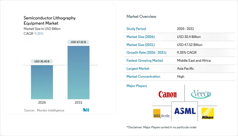
半導体リソグラフィ装置市場は、2025年の278億米ドルから2026年には304億米ドルへ成長し、2026年から2031年にかけてCAGR9.35%で推移し、2031年までに475億2,000万米ドルに達すると予測されています。
この成長の勢いは、極端紫外線(EUV)および今後の高NA EUVプラットフォームへの移行、人工知能サーバーの急増、そしてより高密度なパターニング精度を要求する数兆トランジスタ規模のグラフィックスアクセラレータに起因しています。アジア太平洋地域は、台湾のファウンダリ優位性と韓国の4,710億米ドル規模のメガクラスター計画に牽引され、製造能力拡大の要としての地位を維持しています。深紫外(DUV)装置は成熟ノードの基盤として依然重要ですが、高NA EUV装置の受注パイプラインは、エコシステムが1nm未満の生産へ急速に転換していることを示しています。設備投資の集中度と輸出規制への対応が普及の主な障壁となっていますが、政府補助金、パッケージング技術革新、省エネルギー型装置設計が相まって、先進露光システムの適用範囲を拡大しています。
世界の半導体リソグラフィ装置市場の動向と洞察
微細化プロセスがEUV導入を推進
トランジスタ密度の増加により、EUVのみが達成可能なサブ7nm以下の微細化が求められています。TSMCは2030年までに1nmプロセスの量産化を準備する中で、新竹工場において高NA露光装置のファーストライトを記録しました。ASMLのEXEプラットフォームはアナモルフィック光学系により8nm解像度を達成し、従来のNXEモデルと比較して40%の撮像コントラスト向上を実現しています。調査チームは5nmの線間隔干渉露光を実現し、ロードマップを大幅に下回る能力を確認しました。サーバー級プロセッサは2,000億トランジスタへ倍増すると予測され、リソグラフィーの処理能力需要を拡大させています。これらのマイルストーンは、オングストローム単位の微細化に向けた急速なペースを浮き彫りにし、高NA装置を設備投資の最優先事項に位置づけています。
最先端チップに対するAIおよびデータセンターの需要
人工知能サーバーには、2兆トランジスタを超えるマルチチップGPUが求められます。半導体売上高は2030年までに1兆米ドルを超えると予測され、AIアクセラレータと高帯域メモリが主要な成長エンジンとなります。CoWoSなどの先進的パッケージング技術は、再配線層のリソグラフィオーバーレイ精度をさらに厳しく要求します。サムスンのヘテロジニアス統合ロードマップとTSMCのCoWoS生産能力拡大により、大型パネル露光装置への緊急発注が相次いでおります。数十万台のGPUを擁するアブダビの1~5GW規模AIコンピューティングクラスターは、新たな地域が設備投資サイクルに参入する兆候を示しております。
EUV露光装置の超高額設備投資
ASML社の高NA装置は1台あたり3億8,000万米ドルと、初期EUVプラットフォームの2倍の価格です。クリーンルームの再構築、防振対策、メガワット級の電力・冷却設備により、総所有コストはさらに膨らみます。2025年末までに世界で設置される高NA装置は20台未満と見込まれ、中堅ファブはオングストローム競争から締め出される状況です。沖縄科学技術大学院大学の調査では、2枚のミラーを用いたプロジェクターと20Wの光源を提案しており、これにより電力消費を90%削減できる可能性が示唆され、将来的な設備投資負担の軽減が期待されます。
セグメント分析
2025年、DUVプラットフォームは半導体リソグラフィ装置市場シェアの56.10%を維持し、成熟ノードおよびコスト重視ラインにおける重要性を示しました。高NA EUVは現在半導体リソグラフィ装置市場規模における割合は小さいもの、単一露光による1nmイメージングが量産現実となる2031年までにCAGR10.54%で拡大すると予測されています。ASMLのEXEシリーズに搭載された0.55 NAアナモルフィック投影技術は焦点深度を改善し、従来は4重パターニングなしでは達成不可能だった欠陥密度目標を可能にします。Imecが20nmピッチの金属配線で90%の電気的歩留まりを達成したことは、量産準備が整っていることを裏付けています。
従来のEUVは、5nmロジック、NANDフラッシュ、DRAMリフレッシュにおいて依然として不可欠であり、0.33 NAではマルチパターニングによる許容可能なオーバーレイが得られます。多くのファブで既に償却が完了している深紫外液浸露光は、アナログ、RF、MEMSプロセスにおいてダイ単価の優位性を維持しています。キヤノンのナノインプリントパイロットラインやニコンの液浸露光技術強化はニッチ市場における競合を示唆していますが、ASMLのレチクルフォーマットを中心としたエコシステムへの依存が同社のプラットフォーム優位性を支えています。
地域別分析
2025年のアジア太平洋地域の67.60%というシェアは、台湾、韓国、日本、中国本土に集積するロジック・メモリメガファブを反映しています。韓国の4,710億米ドル規模のクラスターには複数のEUV装置が追加され、日本の政府支援策はTSMCを熊本第2期工場建設へ誘引しています。中国は輸出規制にもかかわらず、国内リソグラフィープロジェクトの拡大に伴い、2024年にはファブ装置全体で490億米ドルを支出しました。
北米は第2位で、CHIPS法の共同出資によりインテル、TSMC、サムスンの米国プロジェクト総額が2,000億米ドルを突破。アリゾナ州のツインファブキャンパスだけで予測期間中に25台以上のEUV露光装置を導入予定。オレゴン、オハイオ、テキサスのファブクラスターは地理的冗長性を拡大し、地域の装置サービス需要を強化します。
中東・アフリカ地域は現時点では規模が小さいもの、12.48%のCAGRを示しています。サウジアラビアの10億サウジアラビア・リヤル規模のベンチャーファンドが国家半導体ハブを支え、UAEのデータセンタープロジェクトは現地での先進パッケージング能力を必要とします。政府間技術移転協定によりタイムラインの短縮が促進されますが、労働力とサプライチェーンの深さは依然として開発上のボトルネックとなっています。
その他の特典:
- エクセル形式の市場予測(ME)シート
- アナリストによる3ヶ月間のサポート
よくあるご質問
目次
第1章 イントロダクション
- 調査の前提条件と市場の定義
- 調査範囲
第2章 調査手法
第3章 エグゼクティブサマリー
第4章 市場情勢
- 市場概要
- 市場促進要因
- 微細化プロセスノードの縮小がEUV導入を促進
- 最先端チップに対するAIおよびデータセンターの需要
- 政府によるファブ補助金(例:CHIPS法)
- 先進パッケージングの急成長(2.5D/3D IC)
- 高NA EUVリフレッシュが装置サイクルを加速
- 化合物半導体リソグラフィー需要
- 市場抑制要因
- EUVスキャナーの超高額な設備投資
- サブシステム供給チェーンのボトルネック
- 持続可能性とエネルギー使用に関する圧力
- 中国への輸出管理規制
- バリューチェーン分析
- 規制情勢
- テクノロジーの展望
- ポーターのファイブフォース分析
- 新規参入業者の脅威
- 供給企業の交渉力
- 買い手の交渉力
- 代替品の脅威
- 競争企業間の敵対関係
- 価格分析
- マクロ経済要因の影響
第5章 市場規模と成長予測
- 印刷方式別
- 深紫外線(DUV)
- 極端紫外線(EUV)
- 高NA EUV
- 用途別
- アドバンスドパッケージング
- MEMSデバイス
- LEDデバイス
- パワー半導体および化合物半導体
- エンドユーザー別
- 専業ファウンダリ
- 統合デバイスメーカー(IDM)
- 半導体受託組立・試験サービス(OSAT)
- 地域別
- 北米
- 米国
- カナダ
- メキシコ
- 南米
- ブラジル
- アルゼンチン
- その他南米
- 欧州
- ドイツ
- 英国
- フランス
- イタリア
- スペイン
- ロシア
- その他欧州地域
- アジア太平洋地域
- 中国
- 日本
- インド
- 韓国
- 東南アジア
- その他アジア太平洋地域
- 中東・アフリカ
- 中東
- サウジアラビア
- アラブ首長国連邦
- トルコ
- その他中東
- アフリカ
- 南アフリカ
- ナイジェリア
- その他アフリカ
- 中東
- 北米
第6章 競合情勢
- 市場集中度
- 戦略的動向
- 市場シェア分析
- 企業プロファイル
- ASML Holding N.V.
- Nikon Corporation
- Canon Inc.
- Shanghai Micro Electronics Equipment(Group)Co., Ltd.
- SUSS MicroTec SE
- EV Group
- Veeco Instruments Inc.
- Onto Innovation Inc.
- JEOL Ltd.
- Neutronix Quintel Inc.
- Mycronic AB
- NuFlare Technology Inc.
- Ushio Inc.
- Ultratech(Veeco)
- Mapper Lithography B.V.
- Visitech AS
- KLA Corporation
- MKS Instruments(Newport)
- Inpria Corp.
- Tamarack Scientific Co.
第7章 市場機会と将来の展望
- 発行日
- 発行
- Mordor Intelligence
- ページ情報
- 英文 123 Pages
- 納期
- 2~3営業日