
|
市場調査レポート
商品コード
1684518
リソグラフィ計測装置市場の機会、成長促進要因、産業動向分析、2025~2034年予測Lithography Metrology Equipment Market Opportunity, Growth Drivers, Industry Trend Analysis, and Forecast 2025 - 2034 |
||||||
カスタマイズ可能
|
|||||||
| リソグラフィ計測装置市場の機会、成長促進要因、産業動向分析、2025~2034年予測 |
|
出版日: 2025年01月02日
発行: Global Market Insights Inc.
ページ情報: 英文 220 Pages
納期: 2~3営業日
|

全表示
- 概要
- 目次
リソグラフィ計測装置の世界市場は、2024年に7億5,500万米ドルに達し、2025年から2034年にかけてCAGR 7.4%という驚異的な成長を遂げる見通しです。
この成長の主因は、スマートフォン、タブレット、ウェアラブル端末などの高度な民生用電子機器に対する需要の急増であり、これらは引き続き世界市場を席巻しています。これらのデバイスは、コンパクトで高性能な集積回路(IC)に依存しており、最先端のリソグラフィ・プロセスに重点を置いています。これらの高度な技術は、消費者や産業界が求める次世代機能を実現するために必要な、より高いチップ密度を達成するために不可欠です。さらに、半導体製造の革新、5G技術の採用、AIアプリケーションへの注目の高まりが、精密計測ソリューションの必要性を煽っています。メーカーは、生産プロセスの精度と効率を優先する業界の進化する要求に応えるため、最先端の機器への投資を増やしています。
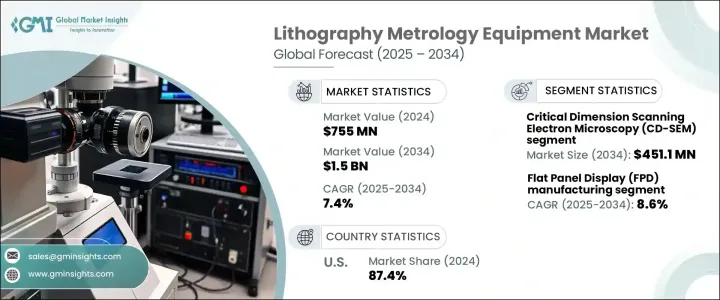
技術別に見ると、市場はオーバーレイ計測、原子間力顕微鏡(AFM)、臨界寸法走査電子顕微鏡(CD-SEM)、光学計測、スキャッタロメトリーに区分されます。その中でもCD-SEMは、2034年までに4億5,110万米ドルの市場規模に達すると予想され、圧倒的な存在感を示しています。CD-SEMはナノスケールの寸法測定において比類のない精度を誇るため、半導体製造に不可欠です。この技術は、マスクパターン、リソグラフィ構造、複雑な設計の検査において比類のない精度を保証し、高度に小型化された複雑な半導体の製造を可能にします。次世代チップに対する需要の高まりは、CD-SEM技術の進歩を後押ししており、業界標準を満たすために、高解像度化、スループットの向上、自動化の強化が強く求められています。
| 市場範囲 | |
|---|---|
| 開始年 | 2024 |
| 予測年 | 2025-2034 |
| 開始金額 | 7億5,500万米ドル |
| 予測金額 | 15億米ドル |
| CAGR | 7.4% |
市場はさらに用途別に分類され、LED製造、半導体製造、フラットパネルディスプレイ(FPD)製造、MEMS(Micro-Electro-Mechanical Systems)製造、その他が含まれます。FPD製造は、2025年から2034年までのCAGRが8.6%で、最も高い成長が予測されています。より大型で高解像度のディスプレイや最先端のOLEDやマイクロLED技術の採用が増加しているため、精密な計測ツールの需要が大幅に高まっています。これらのツールは、層厚、アライメント、解像度を測定し、最適なディスプレイ性能と品質を確保する上で極めて重要な役割を果たしており、エレクトロニクス市場での競争力を維持する上で極めて重要です。
米国では、リソグラフィ計測装置市場が2024年に87.4%のシェアを占めています。同国の優位性は、高度な半導体製造能力と強力な研究開発インフラに起因します。5nm以降を含む最先端ノードへの投資により、EUVリソグラフィと先端計測ソリューションの採用が加速しています。さらに、3Dパッケージング技術への注目の高まりや、AI、IoT、5Gの広範な導入が、米国における革新的で高精度なリソグラフィ計測装置への需要をさらに押し上げています。
目次
第1章 調査手法と調査範囲
- 市場範囲と定義
- 基本推定と計算
- 予測計算
- データソース
- 1次データ
- 2次データ
- 有料情報源
- 公的情報源
第2章 エグゼクティブサマリー
第3章 業界洞察
- エコシステム分析
- バリューチェーンに影響を与える要因
- 利益率分析
- 破壊
- 将来の展望
- メーカー
- 流通業者
- サプライヤーの状況
- 利益率分析
- 主要ニュース
- 規制状況
- 影響要因
- 促進要因
- 半導体技術の進歩
- コンシューマー・エレクトロニクスの需要増加
- 5Gと人工知能(AI)アプリケーションの成長
- 鋳造とメモリー製造への注目の高まり
- 光学および非光学の計測技術の進歩
- 業界の潜在的リスク&課題
- 先端計測機器の高コスト
- 先端ノードの測定の複雑さ
- 促進要因
- 成長可能性分析
- ポーターの分析
- PESTEL分析
第4章 競合情勢
- イントロダクション
- 企業シェア分析
- 競合のポジショニング・マトリックス
- 戦略展望マトリックス
第5章 市場推計・予測:技術別、2021年~2034年
- 主要動向
- 光学計測
- 臨界寸法走査電子顕微鏡(CD-SEM)
- オーバーレイ計測
- 原子間力顕微鏡(AFM)
- 散乱計
第6章 市場推計・予測:製品別、2021年~2034年
- 主要動向
- 化学制御機器
- ガス制御機器
- その他
第7章 市場推計・予測:プロセス別、2021年~2034年
- 主要動向
- エッジ
- クラウド
第8章 市場推計・予測:用途別、2021年~2034年
- 主要動向
- 半導体製造
- フラットパネルディスプレイ(FPD)製造
- MEMS(微小電気機械システム)製造
- LED製造
- その他
第9章 市場推計・予測:最終用途産業別、2021年~2034年
- 主要動向
- 集積デバイスメーカー(IDM)
- 鋳造
第10章 市場推計・予測:地域別、2021-2034年
- 主要動向
- 北米
- 米国
- カナダ
- 欧州
- 英国
- ドイツ
- フランス
- イタリア
- スペイン
- ロシア
- アジア太平洋
- 中国
- インド
- 日本
- 韓国
- オーストラリア
- ラテンアメリカ
- ブラジル
- メキシコ
- 中東・アフリカ
- 南アフリカ
- サウジアラビア
- アラブ首長国連邦
第11章 企業プロファイル
- ASML Holding NV
- Advantest Corporation
- Applied Materials Inc
- Canon Inc.
- Carl Zeiss SMT
- EV Group
- Hitachi High-Tech Corporation
- Holon co Ltd.
- KLA Corporation
- KLA-Tencor
- LAM Research
- Nikon Corporation
- Nova Measuring Instruments Ltd.
- Onto innovation
- Thermo Fisher Scientific Inc.
The Global Lithography Metrology Equipment Market reached USD 755 million in 2024 and is poised to grow at an impressive CAGR of 7.4% between 2025 and 2034. This growth is primarily driven by the surging demand for advanced consumer electronics such as smartphones, tablets, and wearables, which continue to dominate the global market. These devices rely on compact, high-performance integrated circuits (ICs), placing a premium on cutting-edge lithography processes. These advanced techniques are critical for achieving higher chip densities, which are necessary to deliver the next-generation capabilities demanded by consumers and industries alike. Additionally, the rising focus on innovations in semiconductor fabrication, 5G technology adoption, and AI applications is fueling the need for precision metrology solutions. Manufacturers are increasingly investing in state-of-the-art equipment to meet the evolving demands of industries that prioritize accuracy and efficiency in production processes.
By technology, the market is segmented into overlay metrology, Atomic Force Microscopy (AFM), Critical Dimension Scanning Electron Microscopy (CD-SEM), optical metrology, and scatterometry. Among these, CD-SEM is set to dominate, with its market value expected to reach USD 451.1 million by 2034. The unparalleled precision of CD-SEM in measuring nanoscale dimensions makes it indispensable for semiconductor fabrication. This technology ensures unmatched accuracy during the inspection of mask patterns, lithography structures, and intricate designs, enabling the production of highly miniaturized and complex semiconductors. The growing demand for next-generation chips is pushing advancements in CD-SEM technology, with a strong focus on achieving higher resolution, increased throughput, and enhanced automation to meet industry standards.
| Market Scope | |
|---|---|
| Start Year | 2024 |
| Forecast Year | 2025-2034 |
| Start Value | $755 Million |
| Forecast Value | $1.5 Billion |
| CAGR | 7.4% |
The market is further categorized based on applications, which include LED manufacturing, semiconductor manufacturing, Flat Panel Display (FPD) manufacturing, MEMS (Micro-Electro-Mechanical Systems), and others. FPD manufacturing is projected to experience the highest growth, with a CAGR of 8.6% from 2025 to 2034. The rising adoption of larger, high-resolution displays and cutting-edge OLED and microLED technologies has significantly amplified the demand for precise metrology tools. These tools play a pivotal role in measuring layer thickness, alignment, and resolution, ensuring optimal display performance and quality, which are crucial for maintaining a competitive edge in the electronics market.
In the United States, the lithography metrology equipment market accounted for a substantial 87.4% share in 2024. The country's dominance stems from its advanced semiconductor manufacturing capabilities and strong R&D infrastructure. Investments in cutting-edge nodes, including 5nm and beyond, are accelerating the adoption of EUV lithography and advanced metrology solutions. Additionally, the growing focus on 3D packaging technologies and the widespread implementation of AI, IoT, and 5G are further driving the demand for innovative and precise lithography metrology equipment in the United States.
Table of Contents
Chapter 1 Methodology & Scope
- 1.1 Market scope & definitions
- 1.2 Base estimates & calculations
- 1.3 Forecast calculations
- 1.4 Data sources
- 1.4.1 Primary
- 1.4.2 Secondary
- 1.4.2.1 Paid sources
- 1.4.2.2 Public sources
Chapter 2 Executive Summary
- 2.1 Industry synopsis, 2021-2034
Chapter 3 Industry Insights
- 3.1 Industry ecosystem analysis
- 3.1.1 Factor affecting the value chain
- 3.1.2 Profit margin analysis
- 3.1.3 Disruptions
- 3.1.4 Future outlook
- 3.1.5 Manufacturers
- 3.1.6 Distributors
- 3.2 Supplier landscape
- 3.3 Profit margin analysis
- 3.4 Key news & initiatives
- 3.5 Regulatory landscape
- 3.6 Impact forces
- 3.6.1 Growth drivers
- 3.6.1.1 Advancements in semiconductor technology
- 3.6.1.2 Rising demand for consumer electronics
- 3.6.1.3 Growth in 5G and artificial intelligence (AI) applications
- 3.6.1.4 Increasing focus on foundry and memory manufacturing
- 3.6.1.5 Technological advancements in optical and non-optical metrology
- 3.6.2 Industry pitfalls & challenges
- 3.6.2.1 High cost of advanced metrology equipment
- 3.6.2.2 Complexity in measuring advanced nodes
- 3.6.1 Growth drivers
- 3.7 Growth potential analysis
- 3.8 Porter's analysis
- 3.9 PESTEL analysis
Chapter 4 Competitive Landscape, 2024
- 4.1 Introduction
- 4.2 Company market share analysis
- 4.3 Competitive positioning matrix
- 4.4 Strategic outlook matrix
Chapter 5 Market Estimates & Forecast, By Technology, 2021-2034 (USD Million) (Million Units)
- 5.1 Key trends
- 5.2 Optical metrology
- 5.3 Critical dimension scanning electron microscopy (CD-SEM)
- 5.4 Overlay metrology
- 5.5 Atomic force microscopy (AFM)
- 5.6 Scatterometry
Chapter 6 Market Estimates & Forecast, By Product, 2021-2034 (USD Million) (Million Units)
- 6.1 Key trends
- 6.2 Chemical control equipment
- 6.3 Gas control equipment
- 6.4 Others
Chapter 7 Market Estimates & Forecast, By Process, 2021-2034 (USD Million) (Million Units)
- 7.1 Key trends
- 7.2 Edge
- 7.3 Cloud
Chapter 8 Market Estimates & Forecast, By Application, 2021-2034 (USD Million) (Million Units)
- 8.1 Key trends
- 8.2 Semiconductor manufacturing
- 8.3 Flat panel display (FPD) manufacturing
- 8.4 MEMS (micro-electro-mechanical systems)
- 8.5 LED manufacturing
- 8.6 Others
Chapter 9 Market Estimates & Forecast, By End Use Industry, 2021-2034 (USD Million) (Million Units)
- 9.1 Key trends
- 9.2 Integrated Device Manufacturers (IDMs)
- 9.3 Foundries
Chapter 10 Market Estimates & Forecast, By Region, 2021-2034 (USD Million) (Million Units)
- 10.1 Key trends
- 10.2 North America
- 10.2.1 U.S.
- 10.2.2 Canada
- 10.3 Europe
- 10.3.1 UK
- 10.3.2 Germany
- 10.3.3 France
- 10.3.4 Italy
- 10.3.5 Spain
- 10.3.6 Russia
- 10.4 Asia Pacific
- 10.4.1 China
- 10.4.2 India
- 10.4.3 Japan
- 10.4.4 South Korea
- 10.4.5 Australia
- 10.5 Latin America
- 10.5.1 Brazil
- 10.5.2 Mexico
- 10.6 MEA
- 10.6.1 South Africa
- 10.6.2 Saudi Arabia
- 10.6.3 UAE
Chapter 11 Company Profiles
- 11.1 ASML Holding NV
- 11.2 Advantest Corporation
- 11.3 Applied Materials Inc
- 11.4 Canon Inc.
- 11.5 Carl Zeiss SMT
- 11.6 EV Group
- 11.7 Hitachi High-Tech Corporation
- 11.8 Holon co Ltd.
- 11.9 KLA Corporation
- 11.10 KLA-Tencor
- 11.11 LAM Research
- 11.12 Nikon Corporation
- 11.13 Nova Measuring Instruments Ltd.
- 11.14 Onto innovation
- 11.15 Thermo Fisher Scientific Inc.
