
|
市場調査レポート
商品コード
1479764
薄膜形成:動向、重要課題、市場分析Thin Film Deposition: Trends, Key Issues, Market Analysis |
||||||
|
|||||||
| 薄膜形成:動向、重要課題、市場分析 |
|
出版日: 2026年02月01日
発行: Information Network
ページ情報: 英文
納期: 2~3営業日
|

全表示
- 概要
- 図表
- 目次
イントロダクション
半導体産業において、薄膜形成は電子機器の製造プロセスにおいて重要な役割を担っており、半導体基板上に精密かつ制御された材料薄膜層を形成する方法を提供しています。注目すべき複数の動向が、技術の進歩や進化する産業の要件、新しい用途を反映し、半導体薄膜形成市場を形成しています。
第一に、高スループット、均一性、スケーラビリティを提供する薄膜形成技術に対する需要が高まっています。半導体機器がますます複雑化し、集積化されるにつれて、メーカーは大きな基板サイズに対応し、表面積全体にわたって一貫した膜特性を実現できる成膜方法を必要としています。この動向は、原子層堆積法(ALD)や化学気相成長法(CVD)などの革新的な成膜プロセスの開発を後押ししており、大量生産を可能にしながら、膜厚や組成を正確に制御できます。
半導体薄膜形成市場のもう1つの動向は、薄膜形成用の先進材料の採用の増加です。機器の性能要件が上昇を続けるなか、導電性、光透過性、熱安定性などの特性を調整した薄膜に対するニーズが高まっています。この動向は、次世代電子機器の進化する要求に応えるための、新材料の探索に焦点を当てた研究開発活動を後押ししています。
さらに、3次元(3D)半導体構造や異種集積プラットフォームの製作をサポートする薄膜形成技術への注目も高まっています。3D ICやシステムオンチップ(SoC)アーキテクチャのような技術の登場により、非平面上に薄膜を形成し、正確な層間配列を達成できる成膜方法に対するニーズが高まっています。
さらに、薄膜形成技術と、リアルタイムでのプロセス最適化と欠陥検出を可能にするin situモニタリング・制御機能との統合が動向となっています。先進の計測ツールやフィードバック機構を成膜システムに組み込むことで、メーカーはプロセスの安定性、歩留まり、再現性を向上させ、半導体機器の生産コストと市場投入までの時間を削減することができます。
全体として、半導体薄膜形成市場の動向は、優れた性能、機能性、信頼性を備えた先進の電子機器の製造を可能にする革新的なソリューションに対する産業の飽くなき探求を浮き彫りにしています。半導体技術が進化し続ける中、薄膜形成は半導体産業の進歩と革新を推進する重要な実現技術であり続けます。
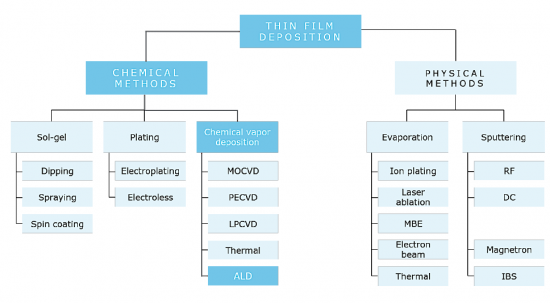
成膜技術の動向
半導体薄膜形成技術の動向は、高精度化、材料の多様化、機器の複雑化、環境の持続可能性、プロセスのインテリジェント化を特徴としています。これらの動向は、新しい成膜方法と材料の開発を形成し、前例のない性能と機能を備えた次世代の電子機器に向けて半導体産業を牽引しています。
半導体薄膜形成技術の情勢は、電子機器の小型化、性能向上、コスト効率のあくなき追求によって、大きく変革しつつあります。この進化は、半導体産業の需要の変化と、これらのニーズを満たすために設計された技術革新を反映する複数の重要な動向によって特徴付けられます。
原子層堆積法(ALD)のような技術は、1度に1原子層ずつ成膜させることができるため、膜厚や組成を比類なく制御することができることから、脚光を浴びています。この精度は、わずかなずれが機器の性能に大きな影響を与える次世代の半導体機器を製造する上で極めて重要です。ALDは複雑な3次元構造をコンフォーマルに成膜できるため、3次元集積回路(IC)や先進メモリ技術などの先進の用途に不可欠です。
従来のシリコンをベースとする半導体は、高誘電体、金属酸化物、グラフェンや遷移金属ジカルコゲナイドのような2次元(2D)材料などのさまざまな新しい材料によって補強されたり、置き換えられたりしています。これらの材料は優れた電気的、熱的、機械的特性を持ち、より高性能で低消費電力の機器の開発を可能にします。これらの材料を取り入れるには、そのユニークな特性と集積化の課題に対応できる成膜技術の進歩が必要です。
当レポートでは、世界の半導体市場について調査分析し、成膜技術情勢の将来見通しを提供しています。また、優先すべき研究課題、解決待ちの技術的課題、予測される市場のシフトを明らかにしています。
目次
第1章 イントロダクション
第2章 エグゼクティブサマリー
第3章 物理蒸着
- イントロダクション
- スパッタリング技術
- プラズマ技術
- リアクター設計
- 半導体プロセス
- ターゲット
第4章 化学蒸着
- イントロダクション
- 化学蒸着(CVD)技術
- APCVD
- LPCVD
- プラズマCVD
- HDPCVD
- ALDA
第5章 電気化学成膜
- イントロダクション
- リアクター設計
- 課題
- 添加物
- 処理
- 銅カソード
- 湿式銅シード層
第6章 成膜と膜特性
- イントロダクション
- 誘電体成膜
- 金属成膜
第7章 ベンダーの問題
- イントロダクション
- 450mm処理
- 統合処理
- 銅
- 計測
- 静電気放電
- パラメトリックテスト
第8章 市場予測
- イントロダクション
- 主な問題
- 市場予測の前提条件
- 市場予測
- 化学蒸着
- 物理蒸着
- 銅電気めっき市場
- ALD市場
List of Figures
- 3.1. Schematic Of Sputtering System
- 3.2. Magnetron Sputtering Design
- 3.3. Showerhead Reactor Design
- 3.4. Ionized PVD
- 4.1. APCVD Reactor
- 4.2. Tube CVD Reactor
- 4.3. HDPCVD Reactor
- 4.4. ALD Versus PVD Copper Barrier
- 5.1. Copper Electroplating System
- 7.1. Comparison Between Semiconductor and Equipment Revenues
- 8.1. Worldwide MCVD Market Shares
- 8.2. Worldwide DCVD Market Shares
- 8.3. Worldwide DCVD Market By Sectors
- 8.4. Worldwide HDHCVD Market Shares
- 8.5. Worldwide PECVD Market Shares
- 8.6. Worldwide SACVD Market Shares
- 8.7. Worldwide LPCVD Market Shares
- 8.8. Worldwide PVD Market Shares
- 8.9. Worldwide ECD Market Shares
- 8.10. Worldwide ALD Market Shares
List of Tables
- 8.1. Worldwide CVD Market Forecast
- 8.2. Worldwide MCVD Market Shares
- 8.3. Worldwide DCVD Market Shares
- 8.4. Worldwide HDPCVD Market Forecast
- 8.5. Worldwide HDPCVD Market Shares
- 8.6. Worldwide PECVD Market Forecast
- 8.7. Worldwide PECVD Market Shares
- 8.8. Worldwide SACVD Market Forecast
- 8.9. Worldwide SACVD Market Shares
- 8.10. Worldwide LPCVD Market Forecast
- 8.11. Worldwide LPCVD Market Shares
- 8.12. Worldwide PVD Market Forecast
- 8.13. Worldwide PVD Market Shares
- 8.14. Worldwide ECD Market Forecast
- 8.15. Worldwide ALD Market Forecast
Introduction
In the semiconductor industry, thin film deposition plays a crucial role in the manufacturing process of electronic devices, providing a method to deposit thin layers of materials onto semiconductor substrates with precision and control. Several notable trends are shaping the semiconductor thin film deposition markets, reflecting advancements in technology, evolving industry requirements, and emerging applications.
Firstly, there is a growing demand for thin film deposition techniques that offer high throughput, uniformity, and scalability. As semiconductor devices become increasingly complex and integrated, manufacturers require deposition methods that can accommodate larger substrate sizes and deliver consistent film properties across the entire surface area. This trend is driving the development of innovative deposition processes, such as atomic layer deposition (ALD) and chemical vapor deposition (CVD), which offer precise control over film thickness and composition while enabling high-volume production.
Another trend in the semiconductor thin film deposition markets is the increasing adoption of advanced materials for thin film deposition. As device performance requirements continue to escalate, there is a growing need for thin films with tailored properties, such as enhanced electrical conductivity, optical transparency, and thermal stability. This trend is driving research and development efforts focused on exploring new materials to meet the evolving demands of next-generation electronic devices.
Furthermore, there is a rising emphasis on thin film deposition techniques that support the fabrication of three-dimensional (3D) semiconductor structures and heterogeneous integration platforms. With the advent of technologies like 3D ICs and system-on-chip (SoC) architectures, there is a growing need for deposition methods capable of depositing thin films on non-planar surfaces and achieving precise layer-to-layer alignment.
Moreover, there is a trend towards the integration of thin film deposition techniques with insitu monitoring and control capabilities, enabling real-time process optimization and defect detection. By incorporating advanced metrology tools and feedback mechanisms into deposition systems, manufacturers can enhance process stability, yield, and reproducibility, thereby reducing production costs and time-to-market for semiconductor devices.
Overall, the trends in the semiconductor thin film deposition markets underscore the industry's ongoing quest for innovative solutions that enable the fabrication of advanced electronic devices with superior performance, functionality, and reliability. As semiconductor technologies continue to evolve, thin film deposition will remain a critical enabling technology, driving progress and innovation in the semiconductor industry.
Trends in Deposition Technology
The trends in semiconductor thin film deposition technology are characterized by a move towards greater precision, material diversity, device complexity, environmental sustainability, and process intelligence. These trends are shaping the development of new deposition methods and materials, driving the semiconductor industry towards the next generation of electronic devices with unprecedented performance and functionality.
The landscape of semiconductor thin film deposition technology is undergoing significant transformation, driven by the relentless pursuit of miniaturization, enhanced performance, and cost-efficiency in electronic devices. This evolution is marked by several key trends that reflect the changing demands of the semiconductor industry and the technological innovations designed to meet these needs.
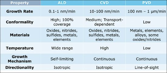
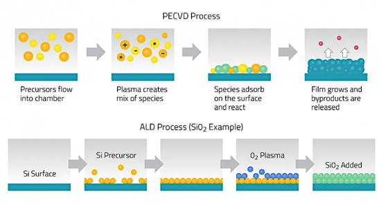
A pivotal trend is the shift towards atomic precision in thin film deposition processes. Techniques such as Atomic Layer Deposition (ALD) are gaining prominence for their ability to deposit films one atomic layer at a time, offering unparalleled control over film thickness and composition. This precision is crucial for manufacturing the next generation of semiconductor devices, where even minor deviations can significantly impact device performance. ALD's ability to conformally coat complex 3D structures makes it indispensable for advanced applications, including 3D integrated circuits (ICs) and advanced memory technologies.
Another significant trend is the diversification of materials used in thin film deposition. Traditional silicon-based semiconductors are being augmented or replaced by a variety of new materials, including high-k dielectrics, metal oxides, and two-dimensional (2D) materials like graphene and transition metal dichalcogenides. These materials offer superior electrical, thermal, and mechanical properties, enabling the development of devices with higher performance and lower power consumption. The incorporation of these materials necessitates advancements in deposition technologies that can handle their unique properties and integration challenges.
The push for greater device integration and functionality is driving the adoption of complex multi-layer structures, which require sophisticated deposition techniques capable of delivering high-quality films with strict interlayer interfaces and uniformity. As devices shrink and the number of layers increases, deposition technologies must offer excellent control over interface engineering, stress management, and layer uniformity to ensure device reliability and performance.
Environmental sustainability and energy efficiency are also becoming critical considerations in thin film deposition processes. The semiconductor industry is increasingly focused on reducing the environmental footprint of manufacturing processes, leading to the development of deposition techniques that consume less energy, use fewer hazardous chemicals, and generate less waste. This trend is not only driven by regulatory pressures but also by the industry's recognition of the importance of sustainable practices for long-term viability.
Lastly, the integration of in-situ monitoring and analytics with deposition processes is a growing trend. Advanced sensors and data analytics are being incorporated directly into deposition systems, enabling real-time process control and optimization. This integration enhances process repeatability, improves yield, and reduces the need for post-deposition inspection, thereby lowering manufacturing costs and improving device performance.
The Need for This Report
This comprehensive semiconductor deposition report provides an in-depth exploration into the multifaceted domain of deposition technologies pivotal to semiconductor manufacturing. It begins with a foundational overview of thin film deposition, shedding light on critical processes such as physical vapor deposition (PVD), chemical vapor deposition (CVD), atomic layer deposition (ALD), and molecular beam epitaxy (MBE). This section demystifies the principles behind each method, offering a comparative analysis to aid in understanding their unique benefits, limitations, and suitability for various semiconductor applications.
Delving into market dynamics, the report presents a detailed examination of global and regional trends, highlighting market growth, demand patterns, and future projections. It paints a comprehensive picture of the competitive landscape, identifying key players, their market positioning, strategic initiatives, and technological breakthroughs. Furthermore, it discusses the impact of regulatory frameworks and environmental standards on deposition practices, emphasizing the industry's response to sustainability and safety mandates.
Technological advancements occupy a central role in the report, showcasing the latest innovations that enhance film quality, deposition efficiency, and material diversity. It highlights the advent of new materials like 2D materials, high-k dielectrics, and metal oxides that promise to revolutionize semiconductor device performance. The narrative extends to the challenges of integrating these advanced deposition processes into mainstream manufacturing, addressing scalability, quality control, and cost-effectiveness.
The application of deposition technologies in fabricating cutting-edge electronic devices is thoroughly analyzed. This includes their role in developing logic chips, memory devices, power electronics, and their contribution to emerging sectors like 3D integrated circuits (ICs), flexible electronics, and solar cells. The report ventures into the future, speculating on the direction of research and development efforts aimed at overcoming existing technological hurdles, enhancing process capabilities, and discovering environmentally friendly deposition methods.
In its concluding sections, the report provides a forward-looking perspective on the deposition technology landscape, identifying research priorities, technological challenges awaiting resolution, and anticipated market shifts. It features case studies and expert opinions to ground its predictions in real-world examples and authoritative insights, offering readers a wellrounded understanding of the current state and future potential of semiconductor deposition technologies.
By weaving together these diverse strands of information, the report serves as a valuable resource for stakeholders across the semiconductor industry spectrum, from manufacturers and researchers to policymakers and investors, equipping them with the knowledge to navigate the complexities of semiconductor deposition in an era of rapid technological change.
About this Report
Thin film deposition processes play a critical role in the production of high-density, highperformance microelectronic products. Considerable progress has been achieved in the development of deposition processes -- and in the development of the reactor systems in which they are carried out. This report discusses relevant mechanisms; processing, system, and materials aspects, potential advances, and considerations regarding extendibility to a wafer diameter of 300 mm and beyond.
With the introduction of new thin-film materials to consistently shrinking microelectronic devices and circuits, and as the aperture ratio of an integrated-circuit structure increases, conformal step coverage becomes increasingly difficult to achieve. This report compares some of the issues impacting users of different deposition tools, including:
|
|
|
In addition, as device geometries shrink, semiconductor manufacturing has become increasingly complex and precise, requiring a better understanding of the specific processes involved. These issues are described in the report.
This report discusses the technology trends, products, applications, and suppliers of materials and equipment. It also gives insights to suppliers for future user needs and should assist them in long range planning, new product development and product improvement. A market forecast for Thin Film Deposition Tools is presented including market shares by deposition type between 2012 and 2023.
Table of Contents
Chapter 1. Introduction
Chapter 2. Executive Summary
Chapter 3. Physical Vapor Deposition
- 3.1. Introduction
- 3.2. Sputtering Technology
- 3.3. Plasma Technology
- 3.4. Reactor Designs
- 3.4.1. Long-Throw Deposition
- 3.4.2. Collimated Sputter Deposition
- 3.4.3. Showerhead Deposition
- 3.4.4. Ionized PVD
- 3.5. Semiconductor Processing
- 3.5.1. Feature Patterning
- 3.5.2. Gap Fill
- 3.6. Targets
Chapter 4. Chemical Vapor Deposition
- 4.1. Introduction
- 4.2. Chemical Vapor Deposition (CVD) Techniques
- 4.2.1. APCVD
- 4.2.2. LPCVD
- 4.2.3. PECVD
- 4.2.4. HDPCVD
- 4.2.5. ALD
Chapter 5. Electrochemical Deposition
- 5.1. Introduction
- 5.2. Reactor Design
- 5.3. Challenges
- 5.4. Additives
- 5.5. Processing
- 5.5.1. Superfilling
- 5.5.2. Aspect Ratios
- 5.6. Copper Cathodes
- 5.7. Wet Copper Seed-Layer
Chapter 6. Film Deposition And Film Properties
- 6.1. Introduction
- 6.2. Dielectric Deposition
- 6.2.1. Silicon Dioxide
- 6.2.1.1. Thermal CVD
- 6.2.1.2. PECVD
- 6.2.1.3. HDPCVD
- 6.2.2. Silicon Nitride
- 6.2.2.1. Thermal CVD
- 6.2.2.2. PECVD
- 6.2.2.3. HDPCVD
- 6.2.3. High-K Dielectrics
- 6.2.4. Low-K Dielectrics
- 6.2.1. Silicon Dioxide
- 6.3. Metal Deposition
- 6.3.1. Aluminum
- 6.3.2. Tungsten/Tungsten Silicide
- 6.3.3. Titanium Nitride
Chapter 7. Vendor Issues
- 7.1. Introduction
- 7.2 450mm Processing
- 7.3. Integrated Processing
- 7.4. Copper
- 7.5. Metrology
- 7.6. ESD
- 7.7. Parametric Test
Chapter 8. Market Forecast
- 8.1. Introduction
- 8.2. Key Issues
- 8.3. Market Forecast Assumptions
- 8.4. Market Forecast
- 8.4.1. Chemical Vapor Deposition
- 8.4.2. Physical Vapor Deposition
- 8.4.3. Copper Electroplating Market
- 8.4.4. Atomic Layer Deposition Market
