
ガリウムヒ素(GaAs)ウェーハの市場機会、成長促進要因、産業動向分析、2025年~2034年予測
Gallium Arsenide (GaAs) Wafer Market Opportunity, Growth Drivers, Industry Trend Analysis, and Forecast 2025 - 2034- 発行日
- ページ情報
- 英文 190 Pages
- 納期
- 2~3営業日
- 商品コード
- 1766204
- カスタマイズ可能 お客様のご希望に応じて、既存データの加工や未掲載情報(例:国別セグメント)の追加などの対応が可能です。詳細はお問い合わせください。
- 翻訳ツール提供対象 PDF対応AI翻訳ツールの無料貸し出しサービスのご利用が可能です
概要
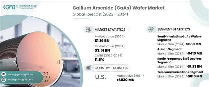
ガリウムヒ素(GaAs)ウェーハの世界市場は、2024年に11億4,000万米ドルと評価され、CAGR 11.8%で成長し、2034年には35億1,000万米ドルに達すると推定されています。
この成長は、5G技術の普及とフォトニクスおよびオプトエレクトロニクスデバイスの進歩によるところが大きいです。ガリウムヒ素は、電子移動度と飽和速度が高いため、シリコンのような従来の材料よりも優れており、高周波や高速のアプリケーションに適しています。5Gインフラの展開が世界的に加速するなか、GaAsウェーハを使って製造されるRFコンポーネントの需要が急増しています。
これらのウェーハは、より高速なデータ転送速度と低遅延をサポートすることで、次世代ワイヤレスシステムに電力を供給するコンポーネントの開発に不可欠です。通信ウェーハとは別に、GaAsウェーハは、効率的な発光と検出をサポートするダイレクトバンドギャップにより、オプトエレクトロニクスアプリケーションで多用されています。通信ネットワークの開発が進むとともに、レーザー技術や光検出器での用途が拡大し、主要経済諸国におけるGaAsウェーハ市場の成長軌道が大幅に強まっています。高性能エレクトロニクスと安全なサプライチェーンへの注目の高まりも、戦略的分野でのウェーハ採用を後押ししています。
| 市場範囲 | |
|---|---|
| 開始年 | 2024 |
| 予測年 | 2025-2034 |
| 開始金額 | 11億4,000万米ドル |
| 予測金額 | 35億1,000万米ドル |
| CAGR | 11.8% |
アジア太平洋地域はGaAsウェーハ生産のハブとして台頭しており、いくつかの国が次世代通信インフラに多額の投資を行い、RFコンポーネントの需要を押し上げています。北米も、5Gの急速な普及と高度なワイヤレスシステムに対するニーズの高まりにより、かなりの勢いを見せています。この地域では、高周波機能を強化するためにGaAsウェーハへの依存が高まっており、最新の通信における戦略的重要性が浮き彫りになっています。このマテリアルハンドリングは、大きなデータストリームを最小限の遅延で処理するのに有効であるため、次世代技術にますます不可欠となっています。一方、世界のオプトエレクトロニクス分野では、ガリウムヒ素の優れた電子移動度とバンドギャップ構造を活用し、LED、レーザーエミッタ、光センサーなどのデバイスへの統合が続いています。
半絶縁性GaAsウエハは2024年に6億8,000万米ドルと評価され、RFおよびマイクロ波コンポーネントの構築に不可欠であるため、市場セグメントをリードしています。キャリア濃度が低く抵抗率が高いため、RFスイッチやアンプの製造に最適で、さまざまな高周波通信プラットフォームで広く使われています。また、信号干渉を最小限に抑えることができるため、精度と性能が要求される環境において最良の選択肢となります。
4インチGaAsウェーハセグメントは、2034年までに4億1,000万米ドルに達すると予測されています。これらのウエハは、製造装置との互換性が確立されており、RFやオプトエレクトロニクスコンポーネントでの使用量が多いことが主な理由です。同市場における長年の存在により、安定した供給チェーンと商業規模の事業への組み込みやすさが保証され、多くのアプリケーションの標準となっています。
米国のガリウムヒ素(GaAs)ウェーハ市場は、防衛、航空宇宙、無線通信分野からの需要増に後押しされ、2034年までに9億3,000万米ドルに達する見込みです。GaAsベースの技術を強化するための官民投資は、国が半導体の独立性と技術的リーダーシップを優先するにつれて加速しています。LIDARや衛星通信のようなアプリケーションでの採用が増え、GaAsウェーハの需要をさらに押し上げています。支援政策と熱心な研究が、この地域の技術革新と国内生産能力の向上を促進しています。
ガリウムヒ素(GaAs)ウェーハ市場を積極的に形成している主要企業には、WIN Semiconductors Corp., IQE plc, Sumitomo Electric Industries, Ltd., VPEC Inc. (Visual Photonics Epitaxy Company), and Toshiba Corporation. などがあります。GaAsウェーハ市場の有力企業は、競争力を維持し、世界のリーチを拡大するために、さまざまな戦略的アプローチを展開しています。各社は、ウェーハの品質向上、生産効率の向上、デバイス性能の強化のため、一貫して研究開発に投資しています。最終用途業界との戦略的提携により、各社は進化する用途ニーズにより合致した製品を提供できるようになっています。また、多くのメーカーが生産能力の拡大に注力しており、サプライチェーンリスクを最小限に抑えながら地域の需要をサポートするため、地域製造ハブを設立しています。さらに、各社は知的財産ポートフォリオを強化し、独自のエピタキシー技術を進化させることで、製品の差別化を図っています。
目次
第1章 調査手法と範囲
第2章 エグゼクティブサマリー
第3章 業界考察
- エコシステム分析
- トランプ政権による関税への影響
- 貿易への影響
- 貿易量の混乱
- 報復措置
- 業界への影響
- 供給側の影響(原材料)
- 主要原材料の価格変動
- サプライチェーンの再構築
- 生産コストへの影響
- 需要側の影響(販売価格)
- 最終市場への価格伝達
- 市場シェアの動向
- 消費者の反応パターン
- 供給側の影響(原材料)
- 影響を受ける主要企業
- 戦略的な業界対応
- サプライチェーンの再構成
- 価格設定と製品戦略
- 政策関与
- 展望と今後の検討事項
- 貿易への影響
- ベンダーマトリックス
- 利益率分析
- テクノロジーとイノベーションの情勢
- 特許分析
- 主なニュースと取り組み
- 業界への影響要因
- 促進要因
- 高周波RFデバイスの需要増加
- オプトエレクトロニクスの応用範囲の拡大
- ADASと自動運転車の成長
- 宇宙および軍事通信における採用
- より大きなウェーハサイズ(6インチ)への移行
- 業界の潜在的リスク&課題
- 高い製造コストと複雑な製造工程
- シリコンとSiGe技術の進歩
- 促進要因
- 成長可能性分析
- 規制情勢
- テクノロジーの情勢
- 将来の市場動向
- ギャップ分析
- ポーター分析
- PESTEL分析
第4章 競合情勢
- イントロダクション
- 企業の市場シェア分析
- 主要市場企業の競合分析
- 競合ポジショニングマトリックス
- 戦略ダッシュボード
第5章 市場推計・予測:ウェーハの種類別、2021年~2034年
- 半絶縁性GaAsウェーハ
- 半導体GaAsウェーハ
第6章 市場推計・予測:ウェーハサイズ別、2021年~2034年
- 2インチ
- 4インチ
- 6インチ
- 8インチ
第7章 市場推計・予測:用途別、2021年~2034年
- 無線周波数(RF)デバイス
- 光電子デバイス
- 太陽光発電装置
- モノリシックマイクロ波集積回路(MMIC)
第8章 市場推計・予測:最終用途別、2021年~2034年
- 通信
- 家電
- 自動車
- 航空宇宙および防衛
- 産業オートメーション
- エネルギーと電力
- その他
第9章 市場推計・予測:地域別、2021年~2034年
- 主要動向
- 北米
- 米国
- カナダ
- 欧州
- ドイツ
- 英国
- フランス
- スペイン
- イタリア
- オランダ
- アジア太平洋地域
- 中国
- インド
- 日本
- オーストラリア
- 韓国
- ラテンアメリカ
- ブラジル
- メキシコ
- アルゼンチン
- 中東・アフリカ
- サウジアラビア
- 南アフリカ
- アラブ首長国連邦
第10章 企業プロファイル
- Analog Devices Inc.
- AWSC(Advanced Wireless Semiconductor Company)
- AXT Inc.
- Broadcom Inc.
- Coherent Corp.
- Cree(Wolfspeed)
- Freiberger Compound Materials GmbH
- Fujitsu Semiconductor Limited
- IntelliEPI Inc.
- IQE plc
- MACOM Technology Solutions
- Northrop Grumman Corporation
- Qorvo Inc.
- RFHIC Corporation
- Skyworks Solutions Inc.
- Sumitomo Electric Industries, Ltd.
- Toshiba Corporation
- VPEC Inc.
- WIN Semiconductors Corp.
目次
The Global Gallium Arsenide Wafer Market was valued at USD 1.14 billion in 2024 and is estimated to grow at a CAGR of 11.8% to reach USD 3.51 billion by 2034. The growth is largely attributed to the widespread adoption of 5G technology and advancements in photonics and optoelectronic devices. Gallium arsenide offers advantages over traditional materials like silicon due to its higher electron mobility and saturation velocity, making it suitable for high-frequency and high-speed applications. As the rollout of 5G infrastructure accelerates globally, the demand for RF components built using GaAs wafers has risen sharply.
These wafers are essential for developing components that power next-gen wireless systems by supporting faster data transfer rates and lower latency. Apart from telecommunications, GaAs wafers are heavily utilized in optoelectronic applications due to their direct bandgap, which supports efficient light emission and detection. The ongoing development in communication networks, along with expanding uses in laser technologies and photodetectors, is significantly strengthening the growth trajectory of the GaAs wafer market across major economies. Increasing focus on high-performance electronics and secure supply chains is also supporting the adoption of these wafers in strategic sectors.
| Market Scope | |
|---|---|
| Start Year | 2024 |
| Forecast Year | 2025-2034 |
| Start Value | $1.14 Billion |
| Forecast Value | $3.51 Billion |
| CAGR | 11.8% |
The Asia-Pacific region is emerging as a hub for GaAs wafer production, with several countries investing heavily in next-generation telecom infrastructure, boosting demand for RF components. North America is also witnessing considerable momentum, driven by rapid 5G adoption and an increasing need for advanced wireless systems. The region's growing reliance on GaAs wafers to enhance high-frequency capabilities highlights their strategic importance in modern communications. The material's effectiveness in handling large data streams with minimal delay is making it increasingly essential to next-gen technologies. Meanwhile, the global optoelectronics sector continues to integrate gallium arsenide into devices like LEDs, laser emitters, and light sensors, leveraging its superior electron mobility and bandgap structure.
Semi-insulating GaAs wafers, valued at USD 680 million in 2024, lead the market segment because they are essential in building RF and microwave components. Their low carrier concentration and high resistivity make them perfect for fabricating RF switches and amplifiers, which are widely used across various high-frequency communication platforms. Their ability to minimize signal interference makes them a top choice in environments demanding precision and performance.
The 4-inch GaAs wafer segment is forecast to reach USD 410 million by 2034. These wafers remain the most preferred in manufacturing, largely because of their established compatibility with production equipment and high usage volumes in RF and optoelectronic components. Their longstanding presence in the market ensures a steady supply chain and ease of integration into commercial-scale operations, making them a standard for many applications.
United States Gallium Arsenide (GaAs) Wafer Market is poised to reach USD 930 million by 2034, fueled by growing demand from defense, aerospace, and wireless communication fields. Public and private investments in enhancing GaAs-based technologies are accelerating as the country prioritizes semiconductor independence and technological leadership. Increasing adoption in applications like LIDAR and satellite communication is further pushing the demand for GaAs wafers. Supportive policies and dedicated research are driving innovation and advancing domestic production capabilities in the region.
Key players actively shaping the Gallium Arsenide (GaAs) Wafer Market include WIN Semiconductors Corp., IQE plc, Sumitomo Electric Industries, Ltd., VPEC Inc. (Visual Photonics Epitaxy Company), and Toshiba Corporation. Prominent players in the GaAs wafer market are deploying a variety of strategic approaches to maintain a competitive edge and expand their global reach. They are consistently investing in R&D to improve wafer quality, increase production efficiency, and enhance device performance. Strategic collaborations with end-use industries are helping companies better align their offerings with evolving application needs. Many manufacturers are also focusing on capacity expansion and establishing regional manufacturing hubs to support local demand while minimizing supply chain risks. In addition, firms are strengthening their intellectual property portfolios and advancing proprietary epitaxy technologies to ensure product differentiation.
Table of Contents
Chapter 1 Methodology and Scope
- 1.1 Market scope and definitions
- 1.2 Research design
- 1.2.1 Research approach
- 1.2.2 Data collection methods
- 1.3 Base estimates and calculations
- 1.3.1 Base year calculation
- 1.3.2 Key trends for market estimation
- 1.4 Forecast model
- 1.5 Primary research and validation
- 1.5.1 Primary sources
- 1.5.2 Data mining sources
Chapter 2 Executive Summary
- 2.1 Industry 3600 synopsis
Chapter 3 Industry Insights
- 3.1 Industry ecosystem analysis
- 3.2 Trump administration tariffs
- 3.2.1 Impact on trade
- 3.2.1.1 Trade volume disruptions
- 3.2.1.2 Retaliatory measures
- 3.2.2 Impact on the industry
- 3.2.2.1 Supply-side impact (raw materials)
- 3.2.2.1.1 Price volatility in key materials
- 3.2.2.1.2 Supply chain restructuring
- 3.2.2.1.3 Production cost implications
- 3.2.2.2 Demand-side impact (selling price)
- 3.2.2.2.1 Price transmission to end markets
- 3.2.2.2.2 Market share dynamics
- 3.2.2.2.3 Consumer response patterns
- 3.2.2.1 Supply-side impact (raw materials)
- 3.2.3 Key companies impacted
- 3.2.4 Strategic industry responses
- 3.2.4.1 Supply chain reconfiguration
- 3.2.4.2 Pricing and product strategies
- 3.2.4.3 Policy engagement
- 3.2.5 Outlook and future considerations
- 3.2.1 Impact on trade
- 3.3 Vendor matrix
- 3.4 Profit margin analysis
- 3.5 Technology & innovation landscape
- 3.6 Patent analysis
- 3.7 Key news and initiatives
- 3.8 Industry impact forces
- 3.8.1 Growth drivers
- 3.8.1.1 Rising demand for high-frequency RF devices
- 3.8.1.2 Expansion of optoelectronics applications
- 3.8.1.3 Growth in ADAS and autonomous vehicles
- 3.8.1.4 Adoption in space and military communications
- 3.8.1.5 Transition to larger wafer sizes (6-inch)
- 3.8.2 Industry pitfalls and challenges
- 3.8.2.1 High manufacturing costs and complex fabrication
- 3.8.2.2 Silicon and SiGe technology advancements
- 3.8.1 Growth drivers
- 3.9 Growth potential analysis
- 3.10 Regulatory landscape
- 3.11 Technology landscape
- 3.12 Future market trends
- 3.13 Gap analysis
- 3.14 Porter's analysis
- 3.15 PESTEL analysis
Chapter 4 Competitive Landscape, 2024
- 4.1 Introduction
- 4.2 Company market share analysis
- 4.3 Competitive analysis of major market players
- 4.4 Competitive positioning matrix
- 4.5 Strategy dashboard
Chapter 5 Market Estimates & Forecast, By Wafer Type, 2021 - 2034 (USD Million)
- 5.1 Semi-insulating GaAs wafers
- 5.2 Semi-conducting GaAs wafers
Chapter 6 Market estimates & forecast, By Wafer Size, 2021 - 2034 (USD Million)
- 6.1 2-inch
- 6.2 4-inch
- 6.3 6-inch
- 6.4 8-inch
Chapter 7 Market Estimates & Forecast, By Application, 2021 - 2034 (USD Million)
- 7.1 Radio frequency (RF) devices
- 7.2 Optoelectronic devices
- 7.3 Photovoltaic devices
- 7.4 Monolithic microwave integrated circuits (MMICs)
Chapter 8 Market estimates & forecast, By End Use, 2021 - 2034 (USD Million)
- 8.1 Telecommunications
- 8.2 Consumer electronics
- 8.3 Automotive
- 8.4 Aerospace & defense
- 8.5 Industrial automation
- 8.6 Energy & power
- 8.7 Others
Chapter 9 Market Estimates and Forecast, By Region, 2021 - 2034 (USD Million)
- 9.1 Key trends
- 9.2 North America
- 9.2.1 U.S.
- 9.2.2 Canada
- 9.3 Europe
- 9.3.1 Germany
- 9.3.2 UK
- 9.3.3 France
- 9.3.4 Spain
- 9.3.5 Italy
- 9.3.6 Netherlands
- 9.4 Asia Pacific
- 9.4.1 China
- 9.4.2 India
- 9.4.3 Japan
- 9.4.4 Australia
- 9.4.5 South Korea
- 9.5 Latin America
- 9.5.1 Brazil
- 9.5.2 Mexico
- 9.5.3 Argentina
- 9.6 Middle East and Africa
- 9.6.1 Saudi Arabia
- 9.6.2 South Africa
- 9.6.3 UAE
Chapter 10 Company Profiles
- 10.1 Analog Devices Inc.
- 10.2 AWSC (Advanced Wireless Semiconductor Company)
- 10.3 AXT Inc.
- 10.4 Broadcom Inc.
- 10.5 Coherent Corp.
- 10.6 Cree (Wolfspeed)
- 10.7 Freiberger Compound Materials GmbH
- 10.8 Fujitsu Semiconductor Limited
- 10.9 IntelliEPI Inc.
- 10.10 IQE plc
- 10.11 MACOM Technology Solutions
- 10.12 Northrop Grumman Corporation
- 10.13 Qorvo Inc.
- 10.14 RFHIC Corporation
- 10.15 Skyworks Solutions Inc.
- 10.16 Sumitomo Electric Industries, Ltd.
- 10.17 Toshiba Corporation
- 10.18 VPEC Inc.
- 10.19 WIN Semiconductors Corp.
- 発行日
- 発行
- Global Market Insights Inc.
- ページ情報
- 英文 190 Pages
- 納期
- 2~3営業日