|
|
市場調査レポート
商品コード
1750314
シリコンEPIウエハーの市場機会、成長促進要因、産業動向分析、2025~2034年予測Silicon EPI Wafer Market Opportunity, Growth Drivers, Industry Trend Analysis, and Forecast 2025 - 2034 |
||||||
|
|||||||
カスタマイズ可能
|
|||||||

| シリコンEPIウエハーの市場機会、成長促進要因、産業動向分析、2025~2034年予測 |
|
出版日: 2025年05月08日
発行: Global Market Insights Inc.
ページ情報: 英文 165 Pages
納期: 2~3営業日
|

全表示
- 概要
- 目次
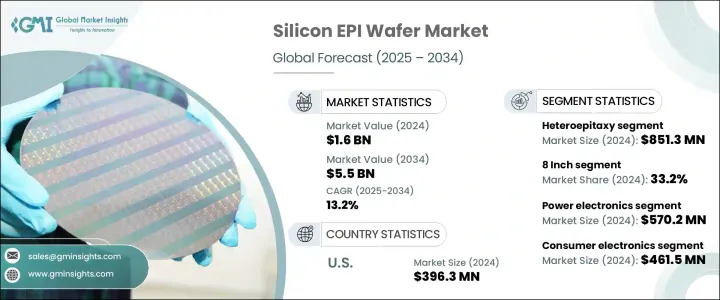
シリコンEPIウエハーの世界市場は、2024年には16億米ドルと評価され、自動車用エレクトロニクス需要の高まり、IoTとエッジコンピューティングデバイスの継続的な展開、世界の半導体製造への巨額投資により、CAGR 13.2%で成長し、2034年には55億米ドルに達すると推定されています。
民生用電子機器、電気自動車、通信などのセグメントでチップ需要が急増する中、エピタキシャルウエハはデバイスの効率化と小型化に貢献しています。先進的なロジックIC、5Gネットワーク、AIベースの技術が採用を加速させている一方で、国の施策支援や産業再集積の取り組みも将来の成長を形作る上で重要な役割を果たしています。
米国では、主要地域からの半導体輸入に対する関税賦課が国内の価格力学を混乱させ、国際競合に影響を及ぼしています。こうした貿易措置は、プラスチック樹脂や特殊金属のような重要なインプットのコストを上昇させ、企業は世界のサプライチェーンの見直しを余儀なくされています。多くの企業が、多額の資本支出を必要とするにもかかわらず、生産拠点の移転や現地化を検討しています。政府による半導体関連法への介入は、国内のウエハー製造能力を高め、新規工場に財政的インセンティブを提供することで、課題の軽減に役立っています。
| 市場範囲 | |
|---|---|
| 開始年 | 2024年 |
| 予測年 | 2025~2034年 |
| 開始金額 | 16億米ドル |
| 予測金額 | 55億米ドル |
| CAGR | 13.2% |
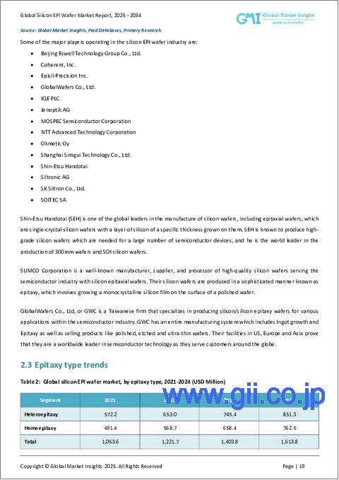
ヘテロエピタキシーセグメントは、オプトエレクトロニクス、RFコンポーネント、先端CMOS技術における高性能半導体デバイスへのニーズの高まりに牽引され、2024年に8億5,130万米ドルを生み出しました。シリコン上のシリコン-ゲルマニウムのように、異なる格子構造を持つ材料をレイヤー化するヘテロエピタキシー能力は、パワー、スピード、サイズに敏感な用途において設計の柔軟性を高めています。3D集積とシステムオンチップアーキテクチャが普及するにつれ、エネルギー効率と小型化の目標を達成するために、ヘテロエピタキシャルプロセスの役割はさらに不可欠になると考えられます。
8インチウエハの2024年の市場シェアは33.2%です。民生用電子機器や自動車用半導体の生産に広く使用されているため、このウエハーサイズが主力となっています。これらのウエハは、特にスマートデバイスや電気自動車に搭載されるパワーデバイスやセンサのコスト効率の高い大量生産を支えています。産業がデジタル化とよりスマートなシステムへとシフトするにつれ、8インチウエハベースのデバイスの需要は増加の一途をたどっています。
米国シリコンEPIウエハー市場は2024年に3億9,630万米ドルを創出、国内チップ製造への連邦政府の強力な投資、EV生産の増加、AIとHPC技術の統合の高まりが後押し。5G、IC製造、自動車エレクトロニクスにおける先進的用途は、特に企業が海外サプライヤーへの依存を減らし、弾力的な地域エコシステムを構築しようとしていることから、国内需要を押し上げます。
世界のシリコンEPIウエハー市場の主要参入企業には、信越半導体(SEH)、Siltronic AG、SUMCO Corporation、SK Siltron Co., Ltd.、GlobalWafers Co., Ltd.などが含まれます。市場での存在感を高めるため、主要企業は生産能力の拡大、技術革新、垂直統合に焦点を当てた戦略を採用しています。各社は、製造能力のアップグレードに多額の投資を行い、次世代デバイスに求められる性能基準の進化に対応する新しいウエハー技術を模索しています。半導体メーカーとの戦略的提携は安定した供給契約を保証し、地理的分散は政治的・貿易的混乱に関連するリスクを軽減します。
目次
第1章 調査手法と範囲
第2章 エグゼクティブサマリー
第3章 産業考察
- エコシステム分析
- バリューチェーンに影響を与える要因
- 利益率分析
- ディスラプション
- 将来の展望
- 製造業者
- 販売代理店
- トランプ政権による関税への影響
- 貿易への影響
- 貿易量の混乱
- 報復措置
- 産業への影響
- 供給側の影響(原料)
- 主要原料の価格変動
- サプライチェーンの再構築
- 生産コストへの影響
- 需要側の影響(販売価格)
- 最終市場への価格伝達
- 市場シェアの動向
- 消費者の反応パターン
- 供給側の影響(原料)
- 影響を受ける主要企業
- 戦略的な産業対応
- サプライチェーンの再構成
- 価格設定と製品戦略
- 施策関与
- 展望と今後の検討事項
- 貿易への影響
- サプライヤーの情勢
- 利益率分析
- 主要ニュースと取り組み
- 規制情勢
- 影響要因
- 促進要因
- 先端半導体デバイスの需要急増
- 自動車エレクトロニクスの拡大
- IoTとエッジデバイスの採用の増加
- 半導体製造への投資の増加
- パワーエレクトロニクス用途の成長
- 産業の潜在的リスク・課題
- エピタキシャル成長の高い資本コストと運用コスト
- 厳格な品質と欠陥管理要件
- 促進要因
- 成長可能性分析
- ポーター分析
- PESTEL分析
第4章 競合情勢
- イントロダクション
- 企業の市場シェア分析
- 競合ポジショニングマトリックス
- 戦略的展望マトリックス
第5章 市場推定・予測:エピタキシータイプ別、2021~2034年
- 主要動向
- ヘテロエピタキシー
- ホモエピタキシー
第6章 市場推定・予測ウエハーサイズ別、2021~2034年
- 主要動向
- 6インチ
- 8インチ
- 12インチ
- その他
第7章 市場推定・予測:用途別、2021~2034年
- 主要動向
- パワーエレクトロニクス
- MEMS
- RFエレクトロニクス
- フォトニクス
- その他
第8章 市場推定・予測:最終用途別、2021~2034年
- 主要動向
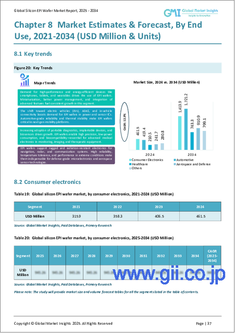
- 民生用電子機器
- 自動車
- ヘルスケア
- 航空宇宙と防衛
- その他
第9章 市場推定・予測:地域別、2021~2034年
- 主要動向
- 北米
- 米国
- カナダ
- 欧州
- 英国
- ドイツ
- フランス
- イタリア
- スペイン
- ロシア
- アジア太平洋
- 中国
- インド
- 日本
- 韓国
- オーストラリア
- ラテンアメリカ
- ブラジル
- メキシコ
- 中東・アフリカ
- 南アフリカ
- サウジアラビア
- アラブ首長国連邦
第10章 企業プロファイル
- Beijing Eswell Technology Group Co.、Ltd.
- Coherent、Inc.
- Episil-Precision Inc.
- GlobalWafers Co.、Ltd.
- IQE PLC
- Jenoptik AG
- MOSPEC Semiconductor Corporation
- NTT Advanced Technology Corporation
- Okmetic Oy
- Shanghai Simgui Technology Co.、Ltd.
- Shin-Etsu Handotai
- Siltronic AG
- SK Siltron Co.、Ltd.
- SOITEC SA
- SRI International
- SUMCO Corporation
- SweGaN AB
- Wafer Works Corporation
- Xiamen Powerway Advanced Material Co.、Ltd
The Global Silicon EPI Wafer Market was valued at USD 1.6 billion in 2024 and is estimated to grow at a CAGR of 13.2% to reach USD 5.5 billion by 2034, driven by rising demand for automotive electronics, the continued rollout of IoT and edge computing devices, and massive investments in global semiconductor manufacturing. As chip demand surges across sectors like consumer electronics, electric vehicles, and telecommunications, epitaxial wafers help improve device efficiency and miniaturization. Advanced logic ICs, 5G networks, and AI-based technologies are accelerating adoption, while national policy support and industrial re-shoring efforts also play a crucial role in shaping future growth.
In the United States, the imposition of tariffs on semiconductor imports from key regions has disrupted domestic pricing dynamics and affected global competitiveness. These trade actions have increased costs for critical inputs like plastic resins and specialty metals, forcing companies to reassess global supply chains. Many firms are relocating or considering localizing production despite the heavy capital outlay required. Government intervention through semiconductor-specific legislation is helping mitigate challenges by boosting domestic wafer manufacturing capabilities and offering financial incentives for new plants.
| Market Scope | |
|---|---|
| Start Year | 2024 |
| Forecast Year | 2025-2034 |
| Start Value | $1.6 Billion |
| Forecast Value | $5.5 Billion |
| CAGR | 13.2% |
The heteroepitaxy segment generated USD 851.3 million in 2024, driven by the increasing need for high-performance semiconductor devices in optoelectronics, RF components, and advanced CMOS technology. The ability of heteroepitaxy to layer materials with differing lattice structures, such as silicon-germanium on silicon, offers greater design flexibility in power, speed, and size-sensitive applications. As 3D integration and system-on-chip architectures grow more prevalent, the role of heteroepitaxial processes will become even more essential to meet energy efficiency and miniaturization goals.
The 8-inch wafer category held a 33.2% market share in 2024. Its widespread use in the production of consumer electronics and automotive semiconductors has made this wafer size a mainstay. These wafers support cost-effective mass manufacturing of power devices and sensors, particularly those deployed in smart devices and electric vehicles. As industries shift toward digitalization and smarter systems, the demand for 8-inch wafer-based devices continues to rise.
U.S. Silicon EPI Wafer Market generated USD 396.3 million in 2024, bolstered by strong federal investment in domestic chip fabrication, rising EV production, and the growing integration of AI and HPC technologies. Advanced applications in 5G, IC manufacturing, and automotive electronics boost local demand, especially as companies seek to reduce reliance on overseas suppliers and build resilient regional ecosystems.
Key players in the Global Silicon EPI Wafer Market include Shin-Etsu Handotai (SEH), Siltronic AG, SUMCO Corporation, SK Siltron Co., Ltd., and GlobalWafers Co., Ltd. Strengthening their market presence, leading companies are adopting strategies that focus on capacity expansion, technological innovation, and vertical integration. Firms are heavily investing in upgrading manufacturing capabilities and exploring new wafer technologies that meet the evolving performance standards required for next-generation devices. Strategic collaborations with semiconductor manufacturers ensure steady supply agreements, while geographic diversification reduces risks related to political or trade disruptions.
Table of Contents
Chapter 1 Methodology & Scope
- 1.1 Market scope & definitions
- 1.2 Base estimates & calculations
- 1.3 Forecast calculations
- 1.4 Data sources
- 1.4.1 Primary
- 1.4.2 Secondary
- 1.4.2.1 Paid sources
- 1.4.2.2 Public sources
Chapter 2 Executive Summary
- 2.1 Industry synopsis, 2021-2034
Chapter 3 Industry Insights
- 3.1 Industry ecosystem analysis
- 3.1.1 Factor affecting the value chain
- 3.1.2 Profit margin analysis
- 3.1.3 Disruptions
- 3.1.4 Future outlook
- 3.1.5 Manufacturers
- 3.1.6 Distributors
- 3.2 Trump administration tariffs
- 3.2.1 Impact on trade
- 3.2.1.1 Trade volume disruptions
- 3.2.1.2 Retaliatory measures
- 3.2.1.3 Impact on the industry
- 3.2.1.3.1 Supply-side impact (raw materials)
- 3.2.1.3.1.1 Price volatility in key materials
- 3.2.1.3.1.2 Supply chain restructuring
- 3.2.1.3.1.3 Production cost implications
- 3.2.1.3.2 Demand-side impact (selling price)
- 3.2.1.3.2.1 Price transmission to end markets
- 3.2.1.3.2.2 Market share dynamics
- 3.2.1.3.2.3 Consumer response patterns
- 3.2.1.3.1 Supply-side impact (raw materials)
- 3.2.1.4 Key companies impacted
- 3.2.1.5 Strategic industry responses
- 3.2.1.5.1 Supply chain reconfiguration
- 3.2.1.5.2 Pricing and product strategies
- 3.2.1.5.3 Policy engagement
- 3.2.1.6 Outlook and future considerations
- 3.2.1 Impact on trade
- 3.3 Supplier landscape
- 3.4 Profit margin analysis
- 3.5 Key news & initiatives
- 3.6 Regulatory landscape
- 3.7 Impact forces
- 3.7.1 Growth drivers
- 3.7.1.1 Surge in demand for advanced semiconductor devices
- 3.7.1.2 Expansion of automotive electronics
- 3.7.1.3 Increasing adoption of IoT and edge devices
- 3.7.1.4 Growing investments in semiconductor manufacturing
- 3.7.1.5 Rising growth in power electronics applications
- 3.7.2 Industry pitfalls & challenges
- 3.7.2.1 High capital and operational costs of epitaxial growth
- 3.7.2.2 Stringent quality and defect control requirements
- 3.7.1 Growth drivers
- 3.8 Growth potential analysis
- 3.9 Porter's analysis
- 3.10 PESTEL analysis
Chapter 4 Competitive Landscape, 2024
- 4.1 Introduction
- 4.2 Company market share analysis
- 4.3 Competitive positioning matrix
- 4.4 Strategic outlook matrix
Chapter 5 Market Estimates & Forecast, By Epitaxy Type, 2021-2034 (USD Million & Units)
- 5.1 Key trends
- 5.2 Heteroepitaxy
- 5.3 Homoepitaxy
Chapter 6 Market Estimates & Forecast, By Wafer Size, 2021-2034 (USD Million & Units)
- 6.1 Key trends
- 6.2 6 inch
- 6.3 8 inch
- 6.4 12 inch
- 6.5 Others
Chapter 7 Market Estimates & Forecast, By Application, 2021-2034 (USD Million & Units)
- 7.1 Key trends
- 7.2 Power electronics
- 7.3 MEMS
- 7.4 RF electronics
- 7.5 Photonics
- 7.6 Others
Chapter 8 Market Estimates & Forecast, By End Use, 2021-2034 (USD Million & Units)
- 8.1 Key trends
- 8.2 Consumer electronics
- 8.3 Automotive
- 8.4 Healthcare
- 8.5 Aerospace and defense
- 8.6 Others
Chapter 9 Market Estimates & Forecast, By Region, 2021-2034 (USD Million & Units)
- 9.1 Key trends
- 9.2 North America
- 9.2.1 U.S.
- 9.2.2 Canada
- 9.3 Europe
- 9.3.1 UK
- 9.3.2 Germany
- 9.3.3 France
- 9.3.4 Italy
- 9.3.5 Spain
- 9.3.6 Russia
- 9.4 Asia Pacific
- 9.4.1 China
- 9.4.2 India
- 9.4.3 Japan
- 9.4.4 South Korea
- 9.4.5 Australia
- 9.5 Latin America
- 9.5.1 Brazil
- 9.5.2 Mexico
- 9.6 MEA
- 9.6.1 South Africa
- 9.6.2 Saudi Arabia
- 9.6.3 UAE
Chapter 10 Company Profiles
- 10.1 Beijing Eswell Technology Group Co., Ltd.
- 10.2 Coherent, Inc.
- 10.3 Episil-Precision Inc.
- 10.4 GlobalWafers Co., Ltd.
- 10.5 IQE PLC
- 10.6 Jenoptik AG
- 10.7 MOSPEC Semiconductor Corporation
- 10.8 NTT Advanced Technology Corporation
- 10.9 Okmetic Oy
- 10.10 Shanghai Simgui Technology Co., Ltd.
- 10.11 Shin-Etsu Handotai
- 10.12 Siltronic AG
- 10.13 SK Siltron Co., Ltd.
- 10.14 SOITEC SA
- 10.15 SRI International
- 10.16 SUMCO Corporation
- 10.17 SweGaN AB
- 10.18 Wafer Works Corporation
- 10.19 Xiamen Powerway Advanced Material Co., Ltd
