
レーザーフォトマスクの市場機会、成長促進要因、産業動向分析、2025年~2034年予測
Laser Photomask Market Opportunity, Growth Drivers, Industry Trend Analysis, and Forecast 2025 - 2034- 発行日
- ページ情報
- 英文 156 Pages
- 納期
- 2~3営業日
- 商品コード
- 1721471
- カスタマイズ可能 お客様のご希望に応じて、既存データの加工や未掲載情報(例:国別セグメント)の追加などの対応が可能です。詳細はお問い合わせください。
- 翻訳ツール提供対象 PDF対応AI翻訳ツールの無料貸し出しサービスのご利用が可能です
概要
レーザーフォトマスクの世界市場規模は、2024年に48億米ドルとなり、CAGR 3%で成長し、2034年には64億米ドルに達すると予測されています。
この成長の原動力となっているのは、先端半導体チップセットに対する需要の増加、電子部品の小型化の進行、民生用電子機器の急増です。半導体技術ノードが3nm以下のレベルまで縮小し続ける中、リソグラフィプロセスの精度がより重要になっています。レーザーフォトマスクは、複雑な回路パターンをシリコンウエハー上に正確に転写することを可能にし、この変革に欠かせないものとなっています。このような高精度のニーズが、フォトマスク製造分野での大幅な技術革新と投資に拍車をかけています。
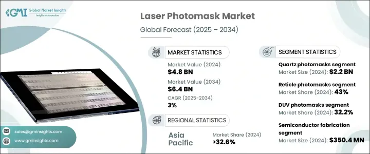
市場は、特に半導体アプリケーションの複雑化に対応して、フォトマスク技術の著しい進歩を目の当たりにしています。チップメーカーが製造の限界に課題するにつれて、高性能フォトマスクへの需要が高まっており、レチクルフォトマスクの2024年の市場規模は20億米ドルです。このセグメントは、最先端のリソグラフィに必要な高解像度パターンの製造に不可欠な役割を果たすため、採用が拡大しています。極端紫外線(EUV)や高NAリソグラフィの台頭により、欠陥のないマスクを確保することが最優先課題となっており、ナノメートル単位で欠陥を検出できるAIベースの検査システムの統合が進んでいます。これにより、生産歩留まりが向上するだけでなく、マスクの修正精度も向上します。
| 市場範囲 | |
|---|---|
| 開始年 | 2024 |
| 予測年 | 2025-2034 |
| 開始金額 | 48億米ドル |
| 予測金額 | 64億米ドル |
| CAGR | 3% |
2024年に22億米ドルを占める石英フォトマスクは、2034年までCAGR 3.2%で成長すると予測され、依然として市場の支配的なセグメントです。石英フォトマスクは、その優れた熱的・光学的特性により、深紫外(DUV)およびEUVリソグラフィプロセスに最適です。最近の進歩には、ハイブリッド石英ブランク構造の使用による光吸収の不均一性の最小化が含まれ、フォトマスクの品質が大幅に向上しています。これは、マスクの忠実度がデバイスの性能に直接影響する、AIプロセッサ、メモリモジュール、その他の高精度電子部品の製造において特に重要です。
米国のレーザーフォトマスク市場は、2024年に10億米ドルを創出し、2034年までCAGR 3.6%で成長すると推定されます。この成長の原動力は、政策的インセンティブと技術進歩に支えられた半導体製造の現地化需要の高まりです。AIを駆使したコンピューティングのニーズが加速することで、先端半導体ノードの需要が高まり、フォトマスクの消費をさらに促進しています。米国内では半導体工場の建設が進んでおり、最先端フォトマスクの需要は引き続き高まると予想されます。
Applied Materials Inc.、Photronics Inc.、KLA Corporationなどの主要企業が市場の最前線にいます。競争力を維持するため、これらの企業は検査工程を合理化し、歩留まりを向上させ、欠陥を最小限に抑える高度な自動化技術やAI技術を採用しています。また、EUV対応フォトマスクの開発に注力し、半導体鋳造メーカーと協力してサブ3nmノードに対応したマスクの開発に取り組んでいます。半導体ハブにおける生産設備の拡張と次世代マスク材料への研究開発費の増加は、拡大する業界の需要に対応し、市場でのリーダーシップを確保するための中心的な戦略です。
目次
第1章 調査手法と範囲
第2章 エグゼクティブサマリー
第3章 業界考察
- エコシステム分析
- ベンダーマトリックス
- 利益率分析
- テクノロジーとイノベーションの情勢
- 特許分析
- 主なニュースと取り組み
- 業界への影響要因
- 促進要因
- 半導体チップセットの需要増加
- 電子部品の急速な小型化
- 家電市場の拡大
- ブランドイメージと市場差別化の強化
- 半導体研究開発への投資増加
- 業界の潜在的リスク&課題
- 高い資本支出と生産コスト
- シリコンサプライチェーンの脆弱性
- 促進要因
- 成長可能性分析
- ポーターの分析
- PESTEL分析
- 将来の市場動向
- 規制情勢
第4章 市場推計・予測:フォトマスクの種類別、2021 –2034
- 主要動向
- レチクルフォトマスク
- マスターフォトマスク
- 複製されたフォトマスク
第5章 市場推計・予測:基材材質別、2021 –2034
- 主要動向
- 石英フォトマスク
- ソーダ石灰フォトマスク
- フィルムフォトマスク
第6章 市場推計・予測:技術別、2021 –2034
- 主要動向
- EUV(極端紫外線)フォトマスク
- DUV(深紫外線)フォトマスク
- バイナリフォトマスク
- 位相シフトフォトマスク
第7章 市場推計・予測:用途別、2021 –2034
- 主要動向
- 半導体製造
- フラットパネルディスプレイ製造
- MEMS(微小電気機械システム)
- ICパッケージング
- オプトエレクトロニクス
- その他
第8章 市場推計・予測:最終用途産業別、2021 –2034
- 主要動向
- 家電
- 自動車
- ヘルスケアおよび医療機器
- 航空宇宙および防衛
- 通信
- その他
第9章 市場推計・予測:地域別、2021–2034
- 主要動向
- 北米
- 米国
- カナダ
- 欧州
- ドイツ
- 英国
- フランス
- スペイン
- イタリア
- その他欧州地域
- アジア太平洋地域
- 日本
- 中国
- インド
- 韓国
- オーストラリア・ニュージーランド
- その他アジア太平洋地域
- ラテンアメリカ
- ブラジル
- メキシコ
- その他ラテンアメリカ地域
- 中東・アフリカ
- 南アフリカ
- アラブ首長国連邦
- サウジアラビア
- その他中東・アフリカ地域
第10章 企業プロファイル
- Applied Materials Inc.
- KLA Corporation
- Photronics Inc.
- Toppan Photomasks、Inc.
- Dai Nippon Printing Co.、Ltd.(DNP)
- Hoya Corporation
- LG Innotek Co.、Ltd.
- SK-Electronics Co.、Ltd.
- Compugraphics
- Nippon Filcon Co.、Ltd.
- Lasertec Corporation
- Taiwan Mask Corporation(TMC)
- Qingyi Photomask Limited
- Hua Hong Semiconductor
- SUSS MicroTec SE
- Mycronic AB
- Carl Zeiss SMT GmbH
- Canon Inc.
- ASML Holding N.V.
- Nikon Corporation
- JEOL Ltd.
- Veeco Instruments Inc.
目次
The Global Laser Photomask Market was valued at USD 4.8 billion in 2024 and is estimated to grow at a CAGR of 3% to reach USD 6.4 billion by 2034. This growth is being driven by the increasing demand for advanced semiconductor chipsets, the ongoing miniaturization of electronic components, and a surge in consumer electronics. As semiconductor technology nodes continue shrinking to sub-3nm levels, precision in lithographic processes has become more critical. Laser photomasks are crucial to this transformation, enabling the accurate transfer of complex circuit patterns onto silicon wafers. This need for precision is fueling significant innovation and investment in the photomask manufacturing sector.
The market is witnessing significant advancements in photomask technology, particularly in response to the growing complexity of semiconductor applications. As chipmakers push the boundaries of fabrication, there is an increasing demand for high-performance photomasks, with the reticle photomask segment valued at USD 2 billion in 2024. This segment is seeing greater adoption due to its essential role in producing the high-resolution patterns needed for cutting-edge lithography. With the rise of extreme ultraviolet (EUV) and high-NA lithography, ensuring defect-free masks has become a top priority, leading to the integration of AI-based inspection systems that can detect defects at the nanometer scale. This not only enhances production yield but also improves mask repair accuracy.
| Market Scope | |
|---|---|
| Start Year | 2024 |
| Forecast Year | 2025-2034 |
| Start Value | $4.8 Billion |
| Forecast Value | $6.4 Billion |
| CAGR | 3% |
Quartz photomasks, accounting for USD 2.2 billion in 2024, remain a dominant segment in the market, projected to grow at a CAGR of 3.2% through 2034. The material's exceptional thermal and optical properties make it ideal for deep ultraviolet (DUV) and EUV lithography processes. Recent advancements include the use of hybrid quartz-blank structures to minimize light absorption inconsistencies, significantly improving the quality of photomasks. This is especially important in the production of AI processors, memory modules, and other high-precision electronic components, where the fidelity of the mask directly affects device performance.
The United States Laser Photomask Market is estimated to generate USD 1 billion in 2024, growing at a CAGR of 3.6% through 2034. This growth is fueled by the rising demand for localized semiconductor manufacturing, supported by policy incentives and technological advances. The accelerating need for AI-powered computing has increased demand for advanced semiconductor nodes, further driving photomask consumption. With the construction of more semiconductor fabs within the U.S., the demand for state-of-the-art photomasks is expected to continue rising.
Leading companies such as Applied Materials Inc., Photronics Inc., and KLA Corporation are at the forefront of the market. To maintain a competitive edge, these companies are adopting advanced automation and AI technologies to streamline inspection processes, improve yield, and minimize defects. They are also focusing on developing EUV-compatible photomasks and collaborating with semiconductor foundries to create masks tailored for sub-3nm nodes. Expanding production facilities in semiconductor hubs and increasing R&D spending on next-gen mask materials are central strategies to meet growing industry demands and secure market leadership.
Table of Contents
Chapter 1 Methodology & Scope
- 1.1 Market scope & definitions
- 1.2 Research design
- 1.2.1 Research approach
- 1.2.2 Data collection methods
- 1.3 Base estimates & calculations
- 1.3.1 Base year calculation
- 1.3.2 Key trends for market estimation
- 1.4 Forecast model
- 1.5 Primary research and validation
- 1.5.1 Primary sources
- 1.5.2 Data mining sources
Chapter 2 Executive Summary
- 2.1 Industry 3600 synopsis
Chapter 3 Industry Insights
- 3.1 Industry ecosystem analysis
- 3.2 Vendor matrix
- 3.3 Profit margin analysis
- 3.4 Technology & innovation landscape
- 3.5 Patent analysis
- 3.6 Key news and initiatives
- 3.7 Industry impact forces
- 3.7.1 Growth drivers
- 3.7.1.1 Growing demand for semiconductor chipsets
- 3.7.1.2 Rapid miniaturization of electronic components
- 3.7.1.3 Expansion of the consumer electronics market
- 3.7.1.4 Enhanced Brand Image and Market Differentiation
- 3.7.1.5 Increased investment in semiconductor R&D
- 3.7.2 Industry pitfalls & challenges
- 3.7.2.1 High capital expenditure and production costs
- 3.7.2.2 Vulnerability to the silicon supply chain
- 3.7.1 Growth drivers
- 3.8 Growth potential analysis
- 3.9 Porter’s analysis
- 3.10 PESTEL analysis
- 3.11 Future market trends
- 3.12 Regulatory landscape
Chapter 4 Market Estimates and Forecast, By Photomask Type, 2021 – 2034 (USD Million & Million Units)
- 4.1 Key trends
- 4.2 Reticle photomasks
- 4.3 Master photomasks
- 4.4 Replicated photomasks
Chapter 5 Market Estimates and Forecast, By Substrate Material, 2021 – 2034 (USD Million & Million Units)
- 5.1 Key trends
- 5.2 Quartz photomasks
- 5.3 Soda-lime photomasks
- 5.4 Film photomasks
Chapter 6 Market Estimates and Forecast, By Technology, 2021 – 2034 (USD Million & Million Units)
- 6.1 Key trends
- 6.2 EUV (Extreme Ultraviolet) photomasks
- 6.3 DUV (Deep Ultraviolet) photomasks
- 6.4 Binary photomasks
- 6.5 Phase shift photomasks
Chapter 7 Market Estimates and Forecast, By Application, 2021 – 2034 (USD Million & Million Units)
- 7.1 Key trends
- 7.2 Semiconductor fabrication
- 7.3 Flat panel display manufacturing
- 7.4 MEMS (Micro-Electromechanical Systems)
- 7.5 IC packaging
- 7.6 Optoelectronics
- 7.7 Other
Chapter 8 Market Estimates and Forecast, By End Use Industry, 2021 – 2034 (USD Million & Million Units)
- 8.1 Key trends
- 8.2 Consumer electronics
- 8.3 Automotive
- 8.4 Healthcare & medical devices
- 8.5 Aerospace & defense
- 8.6 Telecommunication
- 8.7 Others
Chapter 9 Market Estimates and Forecast, By Region, 2021– 2034 (USD Million & Million Units)
- 9.1 Key trends
- 9.2 North America
- 9.2.1 U.S.
- 9.2.2 Canada
- 9.3 Europe
- 9.3.1 Germany
- 9.3.2 UK
- 9.3.3 France
- 9.3.4 Spain
- 9.3.5 Italy
- 9.3.6 Rest of Europe
- 9.4 Asia Pacific
- 9.4.1 Japan
- 9.4.2 China
- 9.4.3 India
- 9.4.4 South Korea
- 9.4.5 ANZ
- 9.4.6 Rest of Asia Pacific
- 9.5 Latin America
- 9.5.1 Brazil
- 9.5.2 Mexico
- 9.5.3 Rest of Latin America
- 9.6 Middle East and Africa
- 9.6.1 South Africa
- 9.6.2 UAE
- 9.6.3 Saudi Arabia
- 9.6.4 Rest of Middle East and Africa
Chapter 10 Company Profiles
- 10.1 Applied Materials Inc.
- 10.2 KLA Corporation
- 10.3 Photronics Inc.
- 10.4 Toppan Photomasks, Inc.
- 10.5 Dai Nippon Printing Co., Ltd. (DNP)
- 10.6 Hoya Corporation
- 10.7 LG Innotek Co., Ltd.
- 10.8 SK-Electronics Co., Ltd.
- 10.9 Compugraphics
- 10.10 Nippon Filcon Co., Ltd.
- 10.11 Lasertec Corporation
- 10.12 Taiwan Mask Corporation (TMC)
- 10.13 Qingyi Photomask Limited
- 10.14 Hua Hong Semiconductor
- 10.15 SUSS MicroTec SE
- 10.16 Mycronic AB
- 10.17 Carl Zeiss SMT GmbH
- 10.18 Canon Inc.
- 10.19 ASML Holding N.V.
- 10.20 Nikon Corporation
- 10.21 JEOL Ltd.
- 10.22 Veeco Instruments Inc.
- 発行日
- 発行
- Global Market Insights Inc.
- ページ情報
- 英文 156 Pages
- 納期
- 2~3営業日


