市場調査レポート
商品コード
1379930

フォトレジストの世界市場 - 世界の産業規模、シェア、動向、機会、予測、2018年~2028年、タイプ別、用途別、地域別、市場競合

Photoresist Market - Global Industry Size, Share, Trends, Opportunity, and Forecast, 2018-2028 Segmented By Type, By Application, By Region and Competition

出版日: | 発行: TechSci Research | ページ情報: 英文 183 Pages | 納期: 2~3営業日

● お客様のご希望に応じて、既存データの加工や未掲載情報(例:国別セグメント)の追加などの対応が可能です。  詳細はお問い合わせください。

価格
価格表記: USDを日本円(税抜)に換算
本日の銀行送金レート: 1USD=157.14円

こちらのレポートには、数時間(ご購入金額の10%)分のアナリストへの質問/追加調査サービスが含まれております。

フォトレジストの世界市場 - 世界の産業規模、シェア、動向、機会、予測、2018年~2028年、タイプ別、用途別、地域別、市場競合
出版日: 2023年10月03日
発行: TechSci Research
ページ情報: 英文 183 Pages
納期: 2~3営業日
  • 全表示
  • 概要
  • 目次
概要

世界のフォトレジストの市場規模は、2022年に37億6,000万米ドルとなり、2028年までの予測期間のCAGRは5.02%で堅調な成長が予測されています。

フォトレジストとリソグラフィプロセスは、最先端の研究から大量生産まで、幅広い先端技術分野で不可欠なものとなっています。これには、IC、MEMS、マイクロエレクトロニクス、マイクロ流体工学、データストレージ技術、バイオテクノロジーなどが含まれます。リソグラフィの分野は目覚ましい進歩を遂げており、ポリマーベースのリソグラフィ手順が広く採用されています。その中でも、電子ビームと光リソグラフィは、学術的にも産業的にも最も一般的に使用されている技術として際立っています。特に光リソグラフィは、マイクロ・ナノファブリケーションに革命をもたらし、100nm以下の高分子構造を大量に製造することを可能にしました。この驚異的な進歩は、レジスト設計、ポリマー、材料製造法、その他の関連技術を開発した多くの科学者や技術者のたゆまぬ努力によって後押しされ、最終的に過去50年にわたるリソグラフィ・プロセスの進化を形作っています。

ナノテクノロジーが広く利用されるようになったことで、MEMSおよびNEMSデバイスの急速な普及への道が開かれました。ナノデバイスは、そのコンパクトなサイズ、軽量性、低消費電力、費用対効果によって人気を集めています。継続的な技術的ブレークスルーに伴い、これらのデバイスの商業化は、フォトレジストとその付属品の市場の展望を大幅に拡大しています。この動向の顕著な例として、インテルが28nmから20nmをベースとする新技術にシフトしたことが挙げられ、半導体産業におけるフォトレジストとその付属品の需要を牽引すると予想されています。

フォトポリマーフォトレジスト、光分解フォトレジスト、光架橋フォトレジストは、フォトレジストに使用される化学構造の一例です。世界の半導体需要の大幅な増加がフォトレジスト需要の急増につながっています。さらに、電気・電子産業では、LCDやOLEDの人気上昇により、フォトレジストの需要が急増しています。さらに、フォトレジストがさまざまな車載アプリケーションに利用される自動車分野の成長も、市場の拡大に拍車をかけると予想されます。これらの要因が総合的にフォトレジスト市場の継続的な成長に寄与しています。

市場概要
予測期間 2024年~2028年
2022年の市場規模 37億6,000万米ドル
2028年の市場規模 50億1,000万米ドル
CAGR 2023年~2028年 5.02%
急成長セグメント 半導体およびIC
最大市場 アジア太平洋

しかし、リソグラフィ工程におけるフォトレジスト材料のコストは、フォトレジストとその付属品の市場成長にとって依然として大きな障壁となっています。このコストは、ICのロジックの複雑さや、レイアウトやエッジの配置エラーの発生状況によって異なります。例えば、NANDロジックは特にコストに敏感であるため、サプライヤーは世代を超えてピッチ分割技術を採用するようになっています。さらに、パターニングは単なるリソグラフィにとどまらず、大量の精密な材料のエンジニアリングを伴うため、製造プロセス全体の中でも複雑かつ重要な要素であることに留意する必要があります。

市場促進要因

MEMSとセンサー需要の増加

フォトレジストは、微小電気機械システム(MEMS)やセンサーの製造を含む、さまざまな微細加工プロセスで使用される感光性材料です。これらのコンポーネントは、スマートフォンやウェアラブル技術から自動車システムや産業機器に至るまで、幅広いデバイスで重要な役割を果たしています。これらの市場が拡大し進化し続けるにつれて、MEMSやセンサー、ひいてはそれらの製造に使用されるフォトレジストの需要は飛躍的に伸びると予想されます。

半導体技術の進歩

世界のフォトレジスト市場は現在大幅な急成長を遂げており、この成長を牽引している重要な要因のひとつが半導体技術の絶え間ない進歩です。世界がますます洗練された電子機器に向かって進歩するにつれ、より小型で効率的な半導体への需要が高まっています。この需要は、間接的にフォトレジストの必要性を煽っています。

フォトレジストは感光性材料であり、様々な表面にパターン化されたコーティングを形成することにより、フォトリソグラフィや写真製版プロセスにおいて重要な役割を果たしています。これらの技術は半導体の製造において最も重要であり、集積回路(IC)やその他のマイクロ電子部品の製造には複雑なパターンが不可欠です。

半導体技術は、ムーアの法則の絶え間ない追求によって、驚異的なスピードで進歩してきました。このよく知られた法則は、チップ上のトランジスタが約2年ごとに倍増することを予言しています。この急速な進歩の結果、これまで以上に小型で効率的な半導体が開発され、強力でコンパクトな電子機器の実現が可能になっています。

さらに、5G、モノのインターネット(IoT)、人工知能(AI)、機械学習といった新たな技術は、半導体技術の限界をさらに押し広げようとしています。これらの技術革新は、これらの最先端技術の計算要求に対応できる高度な半導体の開発を必要としています。

半導体技術の進歩は、世界のフォトレジスト市場に直接的な影響を与えています。より小型で複雑な半導体を製造するために、メーカーはより微細なパターンを高精度で製造できる高度なフォトレジストを必要としています。その結果、高性能フォトレジストへの需要が顕著に増加し、フォトレジスト市場の成長にさらに貢献しています。

結論として、半導体技術の進歩が世界のフォトレジスト市場を牽引する重要な役割を果たしています。半導体技術が進歩し続けるにつれて、高性能フォトレジストへの需要が増加し、フォトレジスト市場の成長を後押しすると予想されます。この継続的な動向は、半導体技術とエレクトロニクス産業全体の将来を形成する上でフォトレジストが極めて重要な役割を担っていることを浮き彫りにしています。

主な市場課題

サプライチェーンの混乱

パンデミックの発生以来、サプライチェーンの混乱は世界経済にとって重要かつ持続的な課題となっています。広範な工場の操業停止は、物流や規制上の障害と相まって、複雑な困難の網の目を作り出し、市場が混乱から回復することを信じられないほど困難にしています。この状況は特にフォトレジスト市場に当てはまり、こうした混乱は生産に大幅な遅れをもたらし、コスト増と競争力低下につながります。

サプライチェーンの混乱がもたらす影響は、個々の業界が直面する当面の課題にとどまりません。様々な分野に波及し、電子機器の心臓部であり頭脳部であるチップの世界の不足を深刻化させる。特にフォトレジスト市場では、チップの複雑な製造工程でフォトレジストが重要な役割を果たしているため、この不足は懸念材料となっています。フォトレジストへの依存は、その可用性とサプライチェーンへのシームレスな統合を、世界中で増大する電子機器の需要に対応するために極めて重要なものにしています。

主な市場動向

環境および規制への対応

フォトレジスト市場における環境と規制の遵守は最も重要です。フォトレジストは、半導体の製造に使用される感光性材料であり、現代のデジタル経済において重要な役割を果たしています。しかし、フォトレジストの製造工程では、環境に影響を与える可能性のある化学物質を使用します。そのため、これらの影響を管理・軽減し、厳しい環境規制を遵守することが、フォトレジスト市場にとって重要な課題となっています。

環境規制の遵守は、環境保護を確実にするだけでなく、生産コストや化学処方の選択にも大きな影響を与えます。規制の厳格化により、規制要件を満たす環境に優しい代替品を見つけるための研究開発に注目が集まっています。現在、多くの企業が、効果的なだけでなく環境にも優しい先進的なフォトレジスト剥離剤の開発に積極的に取り組んでいます。

フォトレジスト市場におけるコンプライアンスの厳格化がもたらす課題により、メーカーは、製品の品質や収益性を損なうことなくこれらの要件を満たすための新たな道や革新的なアプローチを模索するようになりました。この動向に対応するには、多方面からのアプローチが必要です。企業は環境フットプリントを削減するため、グリーン技術や持続可能な慣行に投資し、採用しています。さらに、進化する環境規制を確実に遵守するためには、規制機関との緊密な連携が不可欠です。

環境と規制の遵守に向けたシフトは、フォトレジスト市場においても大きな技術革新を促しています。企業は環境規制に準拠した新製品の開発を迫られており、新技術や持続可能なソリューションの出現につながっています。この動向は、環境への懸念に対応するだけでなく、市場の成長と差別化の機会も提供しています。

結論として、世界のフォトレジスト市場において、環境と規制の遵守は重要かつ継続的な動向です。それは課題をもたらす一方で、革新、成長、持続可能性の機会ももたらします。市場が進化を続ける中、この動向をうまく乗り切り、環境に配慮した慣行を取り入れる企業は、将来的に繁栄し、リードする立場になると思われます。

セグメント別洞察

タイプ別洞察

タイプ別に見ると、2022年のフォトレジスト世界市場では、ARF液浸フォトレジスト分野が圧倒的なシェアを占めています。ArFフォトレジストは、新技術の高度な要件を満たすために様々な産業で広く利用されています。これらのフォトレジストは、光源の最短波長を活用することで、極めて高い解像度を達成することを可能にしています。半導体メーカーが製品の小型化を進める中、ArFフォトレジストへの需要が高まっています。

半導体の分野では、特にLSI(Large Scale Integration)用の回路において、ARF液浸フォトレジストが重要な役割を果たしています。光源の周波数が制限され、屈折率が高いARF液浸フォトレジストを使用することで、フォトレジストユーザーは、性能を向上させた製品の小型化ニーズに応えることができます。さらに、ARFドライフォトレジストに対する需要が増加しており、このコンポーネントの成長をさらに促進しています。

用途別洞察

半導体・IC分野は、予測期間中に急成長すると予測されています。電子ガジェットとしても知られる半導体は、特定の条件下で特定の電気特性を示す材料を用いて製造されます。集積回路(IC)は回路基板の小型版で、抵抗器、コンデンサ、半導体など多数の小さな電子部品で構成されています。これらのICは様々な電子機器に広く使用されており、その需要の拡大が市場の成長に寄与しています。

製造工程では、フォトレジストを使用して、半導体のベースとなるシリコンウエハーの外面に保護層を形成します。さらに、フォトレジスト層を薄くするためにスピンコーティングが一般的に採用されている技術であり、通常、厚さは1マイクロメートル程度です。これにより、半導体上の薄膜の均一性が確保されます。シリコン・ウエハーとスピン・コーティングは、いずれも半導体製造プロセスで重要な役割を果たしています。

半導体需要の高まりは、フォトレジスト市場の成長を後押ししています。電子技術の継続的な進歩に伴い、効率的で高性能な半導体へのニーズは拡大し続けており、市場の進歩・開拓に拍車をかけています。

地域別洞察

2022年のフォトレジスト世界市場では、アジア太平洋地域が金額ベースで最大の市場シェアを占め、支配的なプレーヤーに浮上しました。アジア太平洋地域は、エレクトロニクス産業の最大かつ最速の成長市場として際立っています。この成長は、スマートデバイスの普及やコンシューマーエレクトロニクス需要の増加など、いくつかの要因によるものです。韓国、中国、台湾、インド、日本などのアジア太平洋諸国は、エレクトロニクス産業の成長による需要の増加により、フォトレジスト薬品の地域市場のリーダーとしての地位を確立しており、それが市場全体の発展に拍車をかけています。

特に中国は、世界最大のエレクトロニクス製造拠点を誇り、韓国、シンガポール、台湾といった既存の川上メーカーと激しい競合を繰り広げています。さまざまなコンシューマー・エレクトロニクス・セグメントの中でも、スマートフォン、OLEDテレビ、タブレット端末などのエレクトロニクス製品は、市場の旺盛な需要を反映して、最も高い成長率を示しています。中間層の可処分所得が増加していることから、電子製品に対する需要は予測期間を通じて着実に増加し、市場の成長をさらに促進すると予想されます。さらに、中国の電子機器製造業は、その低い生産コストと電子製品需要の増加により、著しい拡大を経験しています。

目次

第1章 概要

第2章 調査手法

第3章 エグゼクティブサマリー

第4章 世界のフォトレジスト市場の展望

  • 市場規模と予測
    • 金額別
  • 市場シェアと予測
    • タイプ別(ARF液浸フォトレジスト、ARFドライフォトレジスト、KRFフォトレジスト、G線・i線フォトレジスト)
    • 用途別(半導体・IC、LCD、プリント基板、その他)
    • 地域別
    • 企業別(2022年)
  • 市場マップ
    • タイプ別
    • 用途別
    • 地域別

第5章 アジア太平洋のフォトレジスト市場の展望

  • 市場規模・予測
    • 金額別
  • 市場シェアと予測
    • タイプ別
    • 用途別
    • 国別
  • アジア太平洋:国別分析
    • 中国
    • インド
    • オーストラリア
    • 日本
    • 韓国

第6章 欧州のフォトレジスト市場の展望

  • 市場規模・予測
    • 金額別
  • 市場シェアと予測
    • タイプ別
    • 用途別
    • 国別
  • 欧州:国別分析
    • フランス
    • ドイツ
    • スペイン
    • イタリア
    • 英国

第7章 北米のフォトレジスト市場の展望

  • 市場規模・予測
    • 金額別
  • 市場シェアと予測
    • タイプ別
    • 用途別
    • 国別
  • 北米:国別分析
    • 米国
    • メキシコ
    • カナダ

第8章 南米のフォトレジスト市場の展望

  • 市場規模・予測
    • 金額別
  • 市場シェアと予測
    • タイプ別
    • 用途別
    • 国別
  • 南米:国別分析
    • ブラジル
    • アルゼンチン
    • コロンビア

第9章 中東・アフリカのフォトレジスト市場の展望

  • 市場規模・予測
    • 金額別
  • 市場シェアと予測
    • タイプ別
    • 用途別
    • 国別
  • 中東・アフリカ:国別分析
    • 南アフリカ
    • サウジアラビア
    • アラブ首長国連邦
    • エジプト

第10章 市場力学

  • 促進要因
  • 課題

第11章 市場動向と発展

  • 最近の動向
  • 製品上市
  • 合併と買収

第12章 フォトレジストの世界市場SWOT分析

第13章 ポーターのファイブフォース分析

  • 業界内の競合
  • 新規参入の可能性
  • サプライヤーの力
  • 顧客の力
  • 代替品の脅威

第14章 競合情勢

  • ALLRESIST GmbH
    • Business Overview
    • Company Snapshot
    • Products & Services
    • Current Capacity Analysis
    • Financials(In case of listed)
    • Recent Developments
    • SWOT Analysis
  • Asahi Kasei Corporation
  • DJ MicroLaminates, Inc.
  • DuPont de Nemours Inc
  • FUJIFILM Holdings America Corporation
  • JSR Corporation.
  • KOLON Industries, Inc
  • Microchemicals GmbH
  • Sumitomo Chemical Co., Ltd.
  • Shin-Etsu Chemical Co., Ltd.

第15章 戦略的提言

第16章 調査会社について・免責事項

目次
Product Code: 2235

Global Photoresist Market has valued at USD3.76 billion in 2022 and is anticipated to project robust growth in the forecast period with a CAGR of 5.02% through 2028. Photoresists and lithographic processes have become indispensable in a wide range of advanced technological disciplines, from cutting-edge research to high-volume manufacturing. These include ICs, MEMS, microelectronics, microfluidics, data storage technologies, biotechnology, and many more. The field of lithography has witnessed remarkable advancements, with polymer-based lithographic procedures being widely employed. Among these procedures, e-beam and optical lithography stand out as the most commonly used techniques in both academic and industrial settings. Particularly, optical lithography has revolutionized micro and nanofabrication activities, enabling the production of sub-100 nm polymeric structures in large quantities. This incredible progress has been fueled by the relentless efforts of numerous scientists and engineers who have developed resist designs, polymers, material production methods, and other associated technologies, ultimately shaping the evolution of lithographic processes over the last five decades.

The widespread usage of nanotechnology has paved the way for the rapid adoption of MEMS and NEMS devices. Nanodevices are gaining popularity due to their compact size, lightweight nature, low power consumption, and cost-effectiveness. With continuous technical breakthroughs, the commercialization of these devices has significantly expanded the market prospects for photoresist and its ancillaries. One prominent example of this trend is Intel's shift from 28nm to new technologies based on 20nm, which is expected to drive the demand for photoresist and its ancillaries in the semiconductor industry.

Photopolymer photoresist, photo decomposing photoresist, and photo crosslinking photoresist are all examples of the chemical structures used in photoresist. The global demand for semiconductors has witnessed a substantial increase, leading to a surge in the demand for photoresists. Additionally, the electrical and electronics industry is experiencing a boom in demand for photoresists, driven by the rising popularity of LCDs and OLEDs. Moreover, the growing automotive sector, where photoresist is utilized in various in-vehicle applications, is expected to further fuel the market's expansion. These factors collectively contribute to the continuous growth of the photoresist market.

Market Overview
Forecast Period2024-2028
Market Size 2022USD 3.76 Billion
Market Size 2028USD 5.01 Billion
CAGR 2023-20285.02%
Fastest Growing SegmentSemiconductors & ICs
Largest MarketAsia Pacific

However, the cost of photoresist materials in the lithography process remains a significant barrier to market growth for photoresist and its ancillaries. The cost varies based on the logic complexity of ICs and the occurrence of layout and edge placement errors. For instance, NAND logic is particularly cost-sensitive, leading suppliers to adopt pitch division techniques across generations. Furthermore, it is important to note that patterning encompasses more than just lithography; it involves the engineering of a large amount of precise material, making it a complex and critical aspect of the overall manufacturing process.

Key Market Drivers

Rise in Demand of MEMS and Sensors

Photoresists are light-sensitive materials used in various microfabrication processes, including the production of Microelectromechanical Systems (MEMS) and sensors. These components play a critical role in a wide range of devices, ranging from smartphones and wearable technology to automotive systems and industrial equipment. As these markets continue to expand and evolve, the demand for MEMS and sensors, and subsequently the photoresists used in their manufacturing, is expected to grow exponentially.

Given the crucial role of photoresists in the manufacturing of MEMS and sensors, the growth of these markets directly influences the global photoresist market. The increasing demand for wearable and small devices, such as fitness trackers and smartwatches, is acting as a key driver for the consumption of photoresists. Additionally, advancements in medical devices and Internet of Things (IoT) technology are further fueling the demand for MEMS and sensors, thereby contributing to the growth of the photoresist market.

In conclusion, the rise in demand for MEMS and sensors worldwide is driving the growth of the global photoresist market. As technology continues to advance, and the integration of MEMS and sensors into various devices becomes more prevalent, the demand for photoresists is set to increase accordingly. Thus, the future of the photoresist market looks promising, with the rising demand for MEMS and sensors playing a pivotal role in its sustained growth and development.

Advancements in Semiconductor Technology

The global photoresist market is currently experiencing a substantial surge, and one of the key factors driving this growth is the continuous advancements in semiconductor technology. As the world progresses towards increasingly sophisticated electronic devices, there is a growing demand for smaller and more efficient semiconductors. This demand, in turn, indirectly fuels the need for photoresists.

Photoresists are light-sensitive materials that play a crucial role in photolithography and photoengraving processes by forming patterned coatings on various surfaces. These techniques are of utmost importance in the manufacturing of semiconductors, where intricate patterns are essential for the creation of integrated circuits (ICs) and other microelectronic components.

Semiconductor technology has been advancing at an incredible pace, driven by the relentless pursuit of Moore's Law. This well-known principle predicts the doubling of transistors on a chip approximately every two years. As a result of this rapid progression, we have witnessed the development of ever smaller and more efficient semiconductors, enabling the creation of powerful and compact electronic devices.

Moreover, emerging technologies such as 5G, Internet of Things (IoT), artificial intelligence (AI), and machine learning are pushing the boundaries of semiconductor technology even further. These innovations necessitate the development of advanced semiconductors that can handle the computational demands of these cutting-edge technologies.

The advancements in semiconductor technology have a direct impact on the global photoresist market. To create smaller and more complex semiconductors, manufacturers require advanced photoresists capable of producing finer patterns with higher precision. Consequently, there has been a notable increase in the demand for high-performance photoresists, further contributing to the growth of the photoresist market.

In conclusion, the advancements in semiconductor technology are playing a significant role in driving the global photoresist market. As semiconductor technology continues to advance, the demand for high-performance photoresists is expected to increase, thereby bolstering the growth of the photoresist market. This ongoing trend underscores the crucial role of photoresists in shaping the future of semiconductor technology and the electronics industry as a whole.

Key Market Challenges

Disruptions in Supply Chain

Supply chain disruptions have become a significant and persistent challenge for the global economy since the start of the pandemic. The widespread shutdowns of factories, coupled with logistical and regulatory obstacles, have created a complex web of difficulties that have made it incredibly difficult for markets to recover from the disruption. This situation is especially true for the photoresist market, where these disruptions can cause substantial delays in production, leading to increased costs and reduced competitiveness.

The impact of a disrupted supply chain goes beyond the immediate challenges faced by individual industries. It can have cascading effects that ripple through various sectors, exacerbating the global shortage of chips - the very hearts and brains of electronic devices. This shortage is a cause for concern, particularly within the photoresist market, as photoresists play a vital role in the intricate manufacturing process of these chips. The reliance on photoresists makes their availability and seamless integration into the supply chain crucial for meeting the growing demand for electronic devices worldwide.

Key Market Trends

Environmental and Regulatory Compliance

Environmental and regulatory compliance in the photoresist market is of paramount importance. Photoresists, which are light-sensitive materials used in the manufacturing of semiconductors, play a crucial role in our modern digital economy. However, the manufacturing process of photoresists involves the use of chemicals that may have potential environmental impacts. As a result, managing and mitigating these impacts, as well as adhering to stringent environmental regulations, have become critical aspects of the photoresist market.

Compliance with environmental regulations not only ensures the protection of the environment but also has a significant impact on the cost of production and the choice of chemical formulations. Stricter regulations have led to an increased focus on research and development to find environmentally friendly alternatives that meet regulatory requirements. Many companies are now actively developing advanced photoresist strippers that are not only effective but also environmentally friendly.

The challenge posed by stricter compliance measures in the photoresist market has driven manufacturers to explore new avenues and innovative approaches to meet these requirements without compromising on product quality or profitability. Adapting to this trend involves a multi-pronged approach. Companies are investing in and adopting green technologies and sustainable practices to reduce their environmental footprint. Additionally, close collaboration with regulatory bodies is crucial to ensure compliance with evolving environmental regulations.

The shift towards environmental and regulatory compliance has also driven significant innovation in the photoresist market. Companies are being compelled to develop new products that comply with environmental regulations, leading to the emergence of new technologies and sustainable solutions. This trend not only addresses environmental concerns but also provides opportunities for market growth and differentiation.

In conclusion, environmental and regulatory compliance is a significant and ongoing trend in the global photoresist market. While it presents challenges, it also opens up opportunities for innovation, growth, and sustainability. As the market continues to evolve, companies that successfully navigate this trend and embrace environmentally friendly practices will be well-positioned to thrive and lead in the future.

Segmental Insights

Type Insights

Based on the category of type, the ARF Immersion Photoresist segment emerged as the dominant player in the global market for Photoresist in 2022. ArF photoresists are widely utilized in various industries to meet the advanced requirements of new technologies. These photoresists leverage the shortest wavelength of the light source, enabling the achievement of extremely high resolution. As semiconductor manufacturers continue to reduce the size of their products, there is a growing demand for ArF photoresists.

In the field of semiconductors, ARF immersion photoresists play a crucial role, particularly in circuits for Large Scale Integration (LSI). The utilization of ARF immersion photoresist, with its limited frequency of the light source and higher refraction index, allows photoresist users to meet their needs for downsizing products with enhanced performance. Additionally, there is an increasing demand for ARF dry photoresists, further driving the growth of this component.

Application Insights

The Semiconductors & ICs segment is projected to experience rapid growth during the forecast period. Semiconductors, also known as electronic gadgets, are produced using materials that exhibit specific electrical properties under certain conditions. Integrated circuits (ICs) are a smaller version of circuit boards, consisting of numerous tiny electronic components such as resistors, capacitors, and semiconductors. These ICs are widely used in various electronic devices, and the growing demand for such devices contributes to the market's growth.

In the manufacturing process, a photoresist is used to create a protective layer on the outer surface of a silicon wafer, which serves as the base for the semiconductor. Additionally, spin coating is a commonly employed technique to make the photoresist layer thin, typically around 1 micrometer in thickness. This ensures the uniformity of the thin films on the semiconductor. Both the silicon wafer and spin coating play crucial roles in the semiconductor manufacturing process.

The rising demand for semiconductors drives the growth of the photoresist market, as these materials are essential components in semiconductor production. With the continuous advancement in electronic technology, the need for efficient and high-performance semiconductors continues to expand, fueling the market's progress and development.

Regional Insights

Asia Pacific emerged as the dominant player in the Global Photoresist Market in 2022, holding the largest market share in terms of value. The Asia Pacific locale stands out as the largest and fastest-growing market for the electronics industry. This growth can be attributed to several factors, including the widespread adoption of smart devices and the increasing demand for consumer electronics. Countries in the Asia-Pacific region such as South Korea, China, Taiwan, India, and Japan have established themselves as leaders in the regional market for photoresist chemicals due to the growing demand from the thriving electronics industry, which in turn fuels the overall market development.

China, in particular, boasts the world's largest electronics manufacturing base and poses fierce competition to existing upstream manufacturers like South Korea, Singapore, and Taiwan. Among the various consumer electronics segments, electronic products such as smartphones, OLED TVs, and tablets exhibit the highest growth rates, reflecting the strong demand in the market. With the rising disposable income of the middle-class population, the demand for electronic products is expected to steadily increase throughout the forecast period, further driving the market growth. Moreover, China's electronics manufacturing industry is experiencing significant expansion due to its low production costs and the growing demand for electronic goods.

Key Market Players

  • ALLRESIST GmbH
  • Asahi Kasei Corporation
  • DJ MicroLaminates, Inc.
  • DuPont de Nemours Inc
  • FUJIFILM Holdings America Corporation
  • JSR Corporation.
  • KOLON Industries, Inc
  • Microchemicals GmbH
  • Sumitomo Chemical Co., Ltd.
  • Shin-Etsu Chemical Co., Ltd.

Report Scope:

In this report, the Global Photoresist Market has been segmented into the following categories, in addition to the industry trends which have also been detailed below:

Photoresist Market, By Type:

  • ARF Immersion Photoresist
  • ARF Dry Photoresist
  • KRF Photoresist
  • G-Line & I-Line Photoresist

Photoresist Market, By Application:

  • Semiconductors & ICs
  • LCDs
  • Printed Circuit Boards
  • Others

Photoresist Market, By Region:

  • North America
  • United States
  • Canada
  • Mexico
  • Europe
  • France
  • United Kingdom
  • Italy
  • Germany
  • Spain
  • Asia-Pacific
  • China
  • India
  • Japan
  • Australia
  • South Korea
  • South America
  • Brazil
  • Argentina
  • Colombia
  • Middle East & Africa
  • South Africa
  • Saudi Arabia
  • UAE
  • Kuwait
  • Turkey
  • Egypt

Competitive Landscape

  • Company Profiles: Detailed analysis of the major companies present in the Global Photoresist Market.

Available Customizations:

  • Global Photoresist Market report with the given market data, Tech Sci Research offers customizations according to a company's specific needs. The following customization options are available for the report:

Company Information

  • Detailed analysis and profiling of additional market players (up to five).

Table of Contents

1. Product Overview

  • 1.1. Market Definition
  • 1.2. Scope of the Market
    • 1.2.1. Markets Covered
    • 1.2.2. Years Considered for Study
    • 1.2.3. Key Market Segmentations

2. Research Methodology

  • 2.1. Objective of the Study
  • 2.2. Baseline Methodology
  • 2.3. Key Industry Partners
  • 2.4. Major Association and Secondary Sources
  • 2.5. Forecasting Methodology
  • 2.6. Data Triangulation & Validation
  • 2.7. Assumptions and Limitations

3. Executive Summary

  • 3.1. Overview of the Market
  • 3.2. Overview of Key Market Segmentations
  • 3.3. Overview of Key Market Players
  • 3.4. Overview of Key Regions/Countries
  • 3.5. Overview of Market Drivers, Challenges, Trends

4. Global Photoresist Market Outlook

  • 4.1. Market Size & Forecast
    • 4.1.1. By Value
  • 4.2. Market Share & Forecast
    • 4.2.1. By Type (ARF Immersion Photoresist, ARF Dry Photoresist, KRF Photoresist, G-Line & I-Line Photoresist)
    • 4.2.2. By Application (Semiconductors & ICs, LCDs, Printed Circuit Boards, Others)
    • 4.2.3. By Region
    • 4.2.4. By Company (2022)
  • 4.3. Market Map
    • 4.3.1. By Type
    • 4.3.2. By Application
    • 4.3.3. By Region

5. Asia Pacific Photoresist Market Outlook

  • 5.1. Market Size & Forecast
    • 5.1.1. By Value
  • 5.2. Market Share & Forecast
    • 5.2.1. By Type
    • 5.2.2. By Application
    • 5.2.3. By Country
  • 5.3. Asia Pacific: Country Analysis
    • 5.3.1. China Photoresist Market Outlook
      • 5.3.1.1. Market Size & Forecast
        • 5.3.1.1.1. By Value
      • 5.3.1.2. Market Share & Forecast
        • 5.3.1.2.1. By Type
        • 5.3.1.2.2. By Application
    • 5.3.2. India Photoresist Market Outlook
      • 5.3.2.1. Market Size & Forecast
        • 5.3.2.1.1. By Value
      • 5.3.2.2. Market Share & Forecast
        • 5.3.2.2.1. By Type
        • 5.3.2.2.2. By Application
    • 5.3.3. Australia Photoresist Market Outlook
      • 5.3.3.1. Market Size & Forecast
        • 5.3.3.1.1. By Value
      • 5.3.3.2. Market Share & Forecast
        • 5.3.3.2.1. By Type
        • 5.3.3.2.2. By Application
    • 5.3.4. Japan Photoresist Market Outlook
      • 5.3.4.1. Market Size & Forecast
        • 5.3.4.1.1. By Value
      • 5.3.4.2. Market Share & Forecast
        • 5.3.4.2.1. By Type
        • 5.3.4.2.2. By Application
    • 5.3.5. South Korea Photoresist Market Outlook
      • 5.3.5.1. Market Size & Forecast
        • 5.3.5.1.1. By Value
      • 5.3.5.2. Market Share & Forecast
        • 5.3.5.2.1. By Type
        • 5.3.5.2.2. By Application

6. Europe Photoresist Market Outlook

  • 6.1. Market Size & Forecast
    • 6.1.1. By Value
  • 6.2. Market Share & Forecast
    • 6.2.1. By Type
    • 6.2.2. By Application
    • 6.2.3. By Country
  • 6.3. Europe: Country Analysis
    • 6.3.1. France Photoresist Market Outlook
      • 6.3.1.1. Market Size & Forecast
        • 6.3.1.1.1. By Value
      • 6.3.1.2. Market Share & Forecast
        • 6.3.1.2.1. By Type
        • 6.3.1.2.2. By Application
    • 6.3.2. Germany Photoresist Market Outlook
      • 6.3.2.1. Market Size & Forecast
        • 6.3.2.1.1. By Value
      • 6.3.2.2. Market Share & Forecast
        • 6.3.2.2.1. By Type
        • 6.3.2.2.2. By Application
    • 6.3.3. Spain Photoresist Market Outlook
      • 6.3.3.1. Market Size & Forecast
        • 6.3.3.1.1. By Value
      • 6.3.3.2. Market Share & Forecast
        • 6.3.3.2.1. By Type
        • 6.3.3.2.2. By Application
    • 6.3.4. Italy Photoresist Market Outlook
      • 6.3.4.1. Market Size & Forecast
        • 6.3.4.1.1. By Value
      • 6.3.4.2. Market Share & Forecast
        • 6.3.4.2.1. By Type
        • 6.3.4.2.2. By Application
    • 6.3.5. United Kingdom Photoresist Market Outlook
      • 6.3.5.1. Market Size & Forecast
        • 6.3.5.1.1. By Value
      • 6.3.5.2. Market Share & Forecast
        • 6.3.5.2.1. By Type
        • 6.3.5.2.2. By Application

7. North America Photoresist Market Outlook

  • 7.1. Market Size & Forecast
    • 7.1.1. By Value
  • 7.2. Market Share & Forecast
    • 7.2.1. By Type
    • 7.2.2. By Application
    • 7.2.3. By Country
  • 7.3. North America: Country Analysis
    • 7.3.1. United States Photoresist Market Outlook
      • 7.3.1.1. Market Size & Forecast
        • 7.3.1.1.1. By Value
      • 7.3.1.2. Market Share & Forecast
        • 7.3.1.2.1. By Type
        • 7.3.1.2.2. By Application
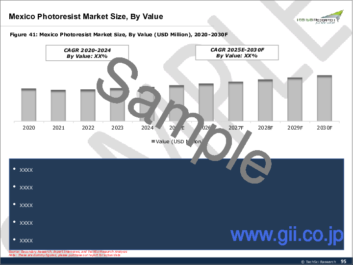
    • 7.3.2. Mexico Photoresist Market Outlook
      • 7.3.2.1. Market Size & Forecast
        • 7.3.2.1.1. By Value
      • 7.3.2.2. Market Share & Forecast
        • 7.3.2.2.1. By Type
        • 7.3.2.2.2. By Application
    • 7.3.3. Canada Photoresist Market Outlook
      • 7.3.3.1. Market Size & Forecast
        • 7.3.3.1.1. By Value
      • 7.3.3.2. Market Share & Forecast
        • 7.3.3.2.1. By Type
        • 7.3.3.2.2. By Application

8. South America Photoresist Market Outlook

  • 8.1. Market Size & Forecast
    • 8.1.1. By Value
  • 8.2. Market Share & Forecast
    • 8.2.1. By Type
    • 8.2.2. By Application
    • 8.2.3. By Country
  • 8.3. South America: Country Analysis
    • 8.3.1. Brazil Photoresist Market Outlook
      • 8.3.1.1. Market Size & Forecast
        • 8.3.1.1.1. By Value
      • 8.3.1.2. Market Share & Forecast
        • 8.3.1.2.1. By Type
        • 8.3.1.2.2. By Application
    • 8.3.2. Argentina Photoresist Market Outlook
      • 8.3.2.1. Market Size & Forecast
        • 8.3.2.1.1. By Value
      • 8.3.2.2. Market Share & Forecast
        • 8.3.2.2.1. By Type
        • 8.3.2.2.2. By Application
    • 8.3.3. Colombia Photoresist Market Outlook
      • 8.3.3.1. Market Size & Forecast
        • 8.3.3.1.1. By Value
      • 8.3.3.2. Market Share & Forecast
        • 8.3.3.2.1. By Type
        • 8.3.3.2.2. By Application

9. Middle East and Africa Photoresist Market Outlook

  • 9.1. Market Size & Forecast
    • 9.1.1. By Value
  • 9.2. Market Share & Forecast
    • 9.2.1. By Type
    • 9.2.2. By Application
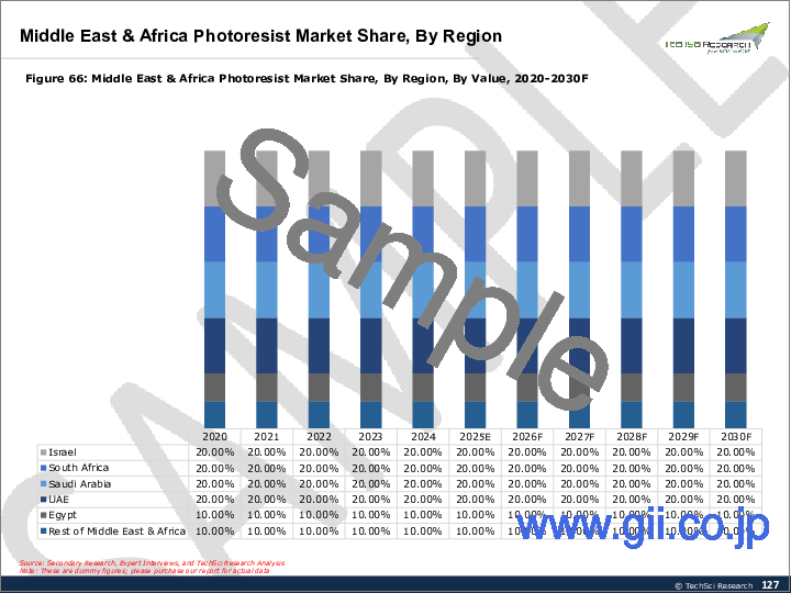
    • 9.2.3. By Country
  • 9.3. MEA: Country Analysis
    • 9.3.1. South Africa Photoresist Market Outlook
      • 9.3.1.1. Market Size & Forecast
        • 9.3.1.1.1. By Value
      • 9.3.1.2. Market Share & Forecast
        • 9.3.1.2.1. By Type
        • 9.3.1.2.2. By Application
    • 9.3.2. Saudi Arabia Photoresist Market Outlook
      • 9.3.2.1. Market Size & Forecast
        • 9.3.2.1.1. By Value
      • 9.3.2.2. Market Share & Forecast
        • 9.3.2.2.1. By Type
        • 9.3.2.2.2. By Application
    • 9.3.3. UAE Photoresist Market Outlook
      • 9.3.3.1. Market Size & Forecast
        • 9.3.3.1.1. By Value
      • 9.3.3.2. Market Share & Forecast
        • 9.3.3.2.1. By Type
        • 9.3.3.2.2. By Application
    • 9.3.4. Egypt Photoresist Market Outlook
      • 9.3.4.1. Market Size & Forecast
        • 9.3.4.1.1. By Value
      • 9.3.4.2. Market Share & Forecast
        • 9.3.4.2.1. By Type
        • 9.3.4.2.2. By Application

10. Market Dynamics

  • 10.1. Drivers
  • 10.2. Challenges

11. Market Trends & Developments

  • 11.1. Recent Developments
  • 11.2. Product Launches
  • 11.3. Mergers & Acquisitions

12. Global Photoresist Market: SWOT Analysis

13. Porter's Five Forces Analysis

  • 13.1. Competition in the Industry
  • 13.2. Potential of New Entrants
  • 13.3. Power of Suppliers
  • 13.4. Power of Customers
  • 13.5. Threat of Substitute Product

14. Competitive Landscape

  • 14.1. ALLRESIST GmbH
    • 14.1.1. Business Overview
    • 14.1.2. Company Snapshot
    • 14.1.3. Products & Services
    • 14.1.4. Current Capacity Analysis
    • 14.1.5. Financials (In case of listed)
    • 14.1.6. Recent Developments
    • 14.1.7. SWOT Analysis
  • 14.2. Asahi Kasei Corporation
  • 14.3. DJ MicroLaminates, Inc.
  • 14.4. DuPont de Nemours Inc
  • 14.5. FUJIFILM Holdings America Corporation
  • 14.6. JSR Corporation.
  • 14.7. KOLON Industries, Inc
  • 14.8. Microchemicals GmbH
  • 14.9. Sumitomo Chemical Co., Ltd.
  • 14.10. Shin-Etsu Chemical Co., Ltd.

15. Strategic Recommendations

16. About Us & Disclaimer