|
|
市場調査レポート
商品コード
1794792
ガラス基板のブレークスルー:CoWoSとCPOイノベーションの推進力Glass Substrate Breakthroughs: Driving CoWoS and CPO Innovation |
||||||
|
|||||||
| ガラス基板のブレークスルー:CoWoSとCPOイノベーションの推進力 |
|
出版日: 2025年07月07日
発行: TrendForce
ページ情報: 英文 16 Pages
納期: 即日から翌営業日
|

全表示
- 概要
- 目次
ガラス基板は、ガラス貫通電極(TGV)技術の最近のブレークスルーにより、先進半導体パッケージングにおいて非常に有望なソリューションとして浮上しています。ガラス基板は、CoWoS、CPO、FOPLP技術の革新を推進する態勢を整えています。優れた高周波性能、低熱膨張係数(CTE)、優れた寸法安定性を活かし、ガラス基板はI/O密度とシグナルインテグリティを大幅に向上させます。このため、大型インターポーザ、多層積層、高周波RFアプリケーションに特に適しています。Intel、Samsung、TSMCなどの大手企業がガラス基板の開発と採用に積極的に投資しているように、TGV技術が広く応用されることで、最先端パッケージング技術の進歩が大きく加速されることになるでしょう。
インフォグラフィックス
主なハイライト
- ガラス基板は、TGV技術のブレークスルーに牽引され、先進半導体パッケージングの主要な新興材料となっています。
- 優れた高周波性能、低熱膨張、優れた寸法安定性を備え、I/O密度とシグナルインテグリティを向上させます。
- 大型インターポーザー、多層スタッキング、高周波RFシナリオに最適です。
- 業界大手はガラス基板開発に投資しており、TGV技術の採用と最先端のパッケージング・イノベーションを加速させています。
目次
第1章 世界のパッケージング動向と基板材料市場概要
第2章 ガラス基板が3D統合の次の波を牽引、コストと性能でTSVに課題
第3章 ガラス基板がCoWoS、CPO、FOPLPを強化し、新たな市場の可能性を解き放つ
第4章 TRIの見解
Glass substrates are emerging as a highly promising solution in advanced semiconductor packaging with recent breakthroughs in Through-Glass Via (TGV) technology. They are poised to drive innovation in CoWoS, CPO, and FOPLP technologies. Leveraging superior high-frequency performance, low coefficient of thermal expansion (CTE), and excellent dimensional stability, glass substrates significantly enhance I/O density and signal integrity. This makes them particularly well-suited for large interposers, multi-layer stacking, and high-frequency RF applications. As major players such as Intel, Samsung and TSMC actively invest in the development and adoption of glass substrates, the widespread application of TGV technology is set to profoundly accelerate the advancement of cutting-edge packaging technologies.
INFOGRAPHICS
Key Highlights:
- Glass substrates, driven by breakthroughs in TGV technology, are key emerging materials for advanced semiconductor packaging.
- They offer superior high-frequency performance, low thermal expansion, and excellent dimensional stability, boosting I/O density and signal integrity.
- Ideally suited for large interposers, multilayer stacking, and high-frequency RF scenarios.
- Major industry players are investing in glass substrate development, accelerating TGV technology adoption and cutting-edge packaging innovation.
Table of Contents
1. Global Packaging Trends and Substrate Material Market Overview
- Table 1: Materials, Technologies, and Key Specifications of FC-BGA and FC-CSP
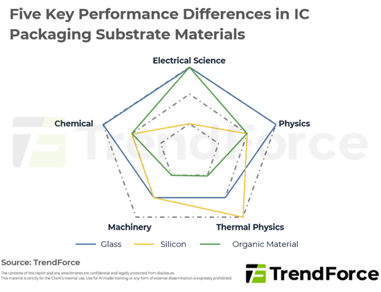
- Figure 1: Five Key Performance Differences in IC Packaging Substrate Materials
- Figure 2: Packaging Architectures Using Silicon, Organic, and Glass Materials
- Table 2: Progress of Substrate and Materials Suppliers in Glass Substrate Development (as of 1H25)
2. Glass Substrates Drive the Next Wave of 3D Integration, Challenging TSV in Cost and Performance
- Table 3: Cost-Effectiveness Comparison of TGV Fabrication Techniques
- Figure 3: Glass Substrates Can Be Applied at Scale in 2.5D/3D Packaging Types
