
|
市場調査レポート
商品コード
1939711
半導体エッチング装置:市場シェア分析、業界動向と統計、成長予測(2026年~2031年)Semiconductor Etch Equipment - Market Share Analysis, Industry Trends & Statistics, Growth Forecasts (2026 - 2031) |
||||||
カスタマイズ可能
適宜更新あり
|
|||||||
| 半導体エッチング装置:市場シェア分析、業界動向と統計、成長予測(2026年~2031年) |
|
出版日: 2026年02月09日
発行: Mordor Intelligence
ページ情報: 英文 150 Pages
納期: 2~3営業日
|

概要
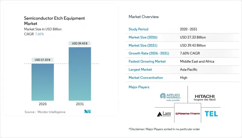
半導体エッチング装置市場は、2025年の254億米ドルから2026年には273億3,000万米ドルへ成長し、2026年から2031年にかけてCAGR7.60%で推移し、2031年までに394億3,000万米ドルに達すると予測されています。
この成長は、先進プロセスノードにおける持続的な設備投資、ゲートオールアラウンドトランジスタの採用加速、およびヘテロジニアス統合の広範な展開を反映しています。人工知能ワークロードの増加、電気自動車生産の拡大、国家補助プログラムが設置済み装置の潜在市場規模を拡大し続ける一方、持続的なヘリウム不足と輸出管理規制が投資のタイミングに影響を与えています。ロジックおよびマイクロプロセッサ製造工場は、出荷台数で最大のシェアを占める最も装置集約的な顧客であり続けていますが、データセンター事業者がより高い帯域幅と改善されたエネルギー効率を必要とするため、高帯域幅メモリおよび先進パッケージングラインが最も速い台数成長を記録しています。原子層エッチングプラットフォームは最高の収益成長率を示していますが、誘導結合プラズマ装置はスループットと化学的柔軟性のため、依然として大量生産ラインの基盤となっています。地域別では、アジア太平洋地域が設置容量を支配していますが、北米、欧州、中東における補助金支援のファブプロジェクトにより、半導体エッチング装置市場の地理的分布は着実に多様化しています。
世界の半導体エッチング装置市場の動向と展望
3nmノード以下の装置微細化
ロジック回路の微細化が進む中、ファブではプラズマ誘発損傷を抑えつつ原子レベルの寸法制御を実現するエッチング装置の導入が求められています。サムスンの3nmゲートオールアラウンドデバイス量産化やTSMCのN2プロセス認定により、材料を単分子層単位で除去する原子層エッチングチャンバーへの即時需要が高まっています。アプライドマテリアルズ社とラムリサーチ社は、独自のパルスプラズマサイクルとインサチュメトリー技術によりサブナノメートルレベルの変動率予算を達成しており、小規模ベンダーが同等の研究開発資金を調達するのに苦労する中、競争上の優位性を強化しています。インテル社の18Aロードマップでは、さらに厳密なプロファイル制御が要求され、これらのノードに対応するサプライヤーにとって複数年にわたる需要の見通しが確固たるものとなっています。ノード移行に伴い、高誘電率絶縁体やルテニウムバリア層などへのフィルム積層化が進む中、差別化された化学処理技術はファブ側の切り替えコストをさらに高め、主要装置メーカーの価格決定力を強化しています。
中国ファウンダリの急速な生産能力拡大
中国のロジックおよび特殊ファウンダリは、業界全体の景気減速にもかかわらず、2024年に月間約20万枚のウエハースタートを追加し、これは世界の増設量の約15%に相当します。政府による資本注入と有利な土地賃貸条件が新規工場建設を加速させる一方、輸出ライセンスの不確実性により、事業者は装置納入を前倒ししています。NAURAなどの国内有力メーカーは中級ノード向けエッチング装置の供給シェアを拡大していますが、最先端ノード向け受注の大半は依然として一流の外国ベンダーが占めています。規制変更を見越した備蓄により、業界全体の停滞期においても四半期ごとの受注高は高水準を維持し、半導体エッチング装置市場は典型的な景気後退の影響を緩和しています。
メモリ分野における設備投資の循環的変動
メモリメーカーは過剰生産能力を是正するため、定期的に設備投資予算を削減します。SKハイニックス、マイクロン、サムスンは供給過剰を受けて2024年初頭にエッチング装置購入を約25%削減し、四半期ごとの装置出荷を抑制しました。3D NAND積層には200回以上のエッチング工程が必要なため、支出の一時停止はエッチング装置サプライヤーの収益に特に大きな影響を与えます。ロジック分野が一部相殺するもの、メモリサイクルの変動幅はベンダーの生産計画に変動をもたらします。
セグメント分析
2025年における半導体エッチング装置市場規模の36.65%をロジック・マイクロプロセッサ製造工場が占め、3nm以下の微細構造への移行速度が最速であることから首位を維持しました。新プロセスノードごとにプロファイル制御精度が要求されるため、ウエハー当たりのエッチング費用が増加します。スマートフォンとデータセンターの継続的な更新サイクルがウエハー生産を後押しする一方、自動車自律運転向けミックスドシグナルチップが生産量に追加貢献しています。メモリ容量の増強は依然として断続的ですが、230層を超える3D NANDは深溝エッチング需要を持続させています。先進パッケージングおよび高帯域幅メモリラインは、2031年までCAGR8.79%で成長すると予測され、ロジックダイと積層DRAMを組み合わせたAIアクセラレータの需要拡大により恩恵を受けています。
ファブレス半導体メーカーがリスク分担モデルを求める中、ファウンダリサービスが注目を集めており、TSMCは2025年末までにCoWoSパッケージングの月産能力を65,000ウエハーに拡大する見込みです。パワーデバイスおよびディスクリートデバイスは、電気自動車用インバーターや急速充電器へのSiCスイッチの採用拡大に伴い加速し、専用の深反応性イオンエッチングシステムを必要とします。MEMSおよびセンサーメーカーは、マイクロフォンアレイやタイヤ空気圧モニター向けに低圧プラズマモジュールを活用しています。新興のフォトニック・量子デバイスは現時点ではニッチ市場ですが、原子レベルのエッチング選択性が要求され、サプライヤーの差別化に新たな道を開いています。
誘導結合プラズマ装置は2025年の収益の33.25%を占め、量産ファブの基幹設備としての地位を確固たるものにしております。幅広い化学処理能力により、単一プラットフォームでポリシリコン、高誘電率絶縁体、金属ゲートに対応可能なため、ライン保守が簡素化されます。反応性イオンエッチング装置は、アスペクト比制約が緩やかな後工程ノードにおいて引き続き採用されております。深部RIE装置はMEMSや貫通シリコンビア(TSV)などの特殊分野を捉え、そのニッチな能力により高利益率を維持しています。
半導体エッチング装置市場がオングストロームレベルの制御へ移行する中、原子層エッチングプラットフォームは9.01%のCAGRで最高成長を記録しています。アプライドマテリアルズ社は、1サイクルあたり単一分子層を除去するパルス高周波ステップを宣伝しています。高アスペクト比モジュールは、60:1を超える3D NANDトレンチに対応し、ここで発生する側壁の反りがセル効率を損なう可能性があります。等方性洗浄やボンディング前表面処理にはウェットベンチシステムが依然として使用されていますが、プラズマ化学処理がより穏やかで選択性を高めるにつれ、その総シェアは低下しています。
地域別分析
アジア太平洋地域は2025年の収益の70.85%を占め、台湾、韓国、中国本土では数十億米ドル規模の生産能力増強が継続しました。TSMCのCoWoS(チップ・オン・ウエハー・オン・ソケット)生産能力が月間6万5,000枚に拡大したことは、先進パッケージング分野における地域の主導性を示しています。一方、サムスンとSKハイニックスのDRAMおよびNANDサイクルは、引き続き大規模なエッチング需要を牽引しています。中国国内ベンダーは急速に学習曲線を登っており、NAURA社の44%の利益成長と世界トップ6入りがこの進展を裏付けています。
北米のシェアは500億米ドルを超えるCHIPS法による優遇措置で支えられています。インテルのオハイオ州200億米ドル規模の建設プロジェクトとTSMCのアリゾナ拠点が大型マルチチャンバーエッチング装置の受注を牽引し、サプライヤーの受注残がアジア依存から分散化しています。欧州のチップス法資金はドイツ、フランス、アイルランドのプロジェクトを推進し、装置出荷の見通しを2020年代末まで拡大しています。
中東・アフリカ地域は、政府による戦略的自律性の追求により、10.74%という最も高い予測CAGRを記録しています。サウジアラビアのNEOMキャンパスやアラブ首長国連邦のクリーンルーム計画では、ターンキーエッチングモジュールを導入するパイロットラインが計画されています。インフラの不足や人材不足は依然として課題ですが、持続的な公的資金が世界のサプライヤーを惹きつけ、半導体エッチング装置市場の地理的基盤をさらに拡大しています。
その他の特典:
- エクセル形式の市場予測(ME)シート
- アナリストによる3ヶ月間のサポート
よくあるご質問
目次
第1章 イントロダクション
- 調査の前提条件と市場の定義
- 調査範囲
第2章 調査手法
第3章 エグゼクティブサマリー
第4章 市場情勢
- 市場概要
- マクロ経済要因の影響
- 業界サプライチェーン分析
- 市場促進要因
- 3nmノード以下の装置微細化
- 中国ファウンダリの急速な生産能力拡大
- ゲート・オール・アラウンド(GAA)トランジスタへの移行
- パワーデバイス分野における300mmから200mmへのリトロフィット需要
- 米国およびEUのファブ補助金支出(CHIPS法)
- ヘテロジニアス統合と先進的パッケージング
- 市場抑制要因
- メモリ分野における設備投資の周期的な変動
- ヘリウム及び希ガス供給の混乱
- 設備平均販売価格の上昇と投資利益率(ROI)の比較
- 輸出管理コンプライアンスコストの増加
- 規制情勢
- テクノロジーの展望
- ポーターのファイブフォース分析
- 新規参入業者の脅威
- 買い手・消費者の交渉力
- 供給企業の交渉力
- 代替品の脅威
- 競争企業間の敵対関係
第5章 市場規模と成長予測
- 用途別
- ロジック/MPU
- メモリ
- ファウンダリサービス
- パワーデバイスおよびディスクリートデバイス
- MEMSおよびセンサー
- 高度なパッケージング/HBM
- その他
- 機器別
- 反応性イオンエッチング装置(RIE)
- 誘導結合プラズマ(ICP)エッチング装置
- 深部反応性イオン(DRIE)
- ウェットエッチングシステム
- 高アスペクト比エッチング(HARP)
- 原子層エッチング(ALE)
- エッチング技術別
- ドライエッチング
- ウェットエッチング
- プロセス別
- フロントエンド・オブ・ライン(FEOL)エッチング
- バックエンド・オブ・ライン(BEOL)エッチング
- 地域
- 北米
- 米国
- カナダ
- メキシコ
- 南米
- ブラジル
- アルゼンチン
- その他南米
- 欧州
- ドイツ
- 英国
- フランス
- イタリア
- スペイン
- ロシア
- その他欧州地域
- アジア太平洋地域
- 中国
- 日本
- インド
- 韓国
- 東南アジア
- その他アジア太平洋地域
- 中東・アフリカ
- 中東
- サウジアラビア
- アラブ首長国連邦
- トルコ
- その他中東
- アフリカ
- 南アフリカ
- ナイジェリア
- その他アフリカ
- 中東
- 北米
第6章 競合情勢
- 市場集中度
- 戦略的動向
- 市場シェア分析
- 企業プロファイル
- Applied Materials, Inc.
- Lam Research Corp.
- Tokyo Electron Ltd.
- Hitachi High-Tech Corp.
- Plasma-Therm LLC
- ASM International N.V.
- NAURA Technology Group Co., Ltd.
- Oxford Instruments Plasma Technology Ltd.
- SPTS Technologies Ltd.(KLA)
- ULVAC, Inc.
- Veeco Instruments Inc.
- SAMCO Inc.
- Advanced Micro-Fabrication Equipment Inc.(AMEC)
- Mattson Technology Inc.
- GlobalFoundries Inc.(In-house Tools)
- Suzhou Ruidow Technology Co., Ltd.
- PVA TePla AG
- CORIAL SAS
- Trion Technology Inc.
- Tescan Orsay Holding a.s.
