
|
市場調査レポート
商品コード
1687460
半導体CVD装置:市場シェア分析、産業動向・統計、成長予測(2025年~2030年)Semiconductor CVD Equipment - Market Share Analysis, Industry Trends & Statistics, Growth Forecasts (2025 - 2030) |
||||||
カスタマイズ可能
適宜更新あり
|
|||||||
| 半導体CVD装置:市場シェア分析、産業動向・統計、成長予測(2025年~2030年) |
|
出版日: 2025年03月18日
発行: Mordor Intelligence
ページ情報: 英文 118 Pages
納期: 2~3営業日
|

全表示
- 概要
- 目次
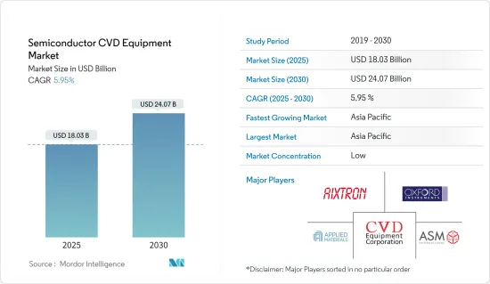
半導体CVD装置の市場規模は2025年に180億3,000万米ドルと推定され、2030年には240億7,000万米ドルに達すると予測され、予測期間(2025-2030年)のCAGRは5.95%です。
マイクロエレクトロニクスベースの消費者製品への需要増加により、半導体、LED、ストレージデバイス産業が急成長しており、電気メッキ用Cr6の使用に対する厳しい規制が主にCVD装置市場の成長を牽引しています。
主なハイライト
- 化学気相成長(CVD)プロセスは、半導体の製造や薄膜の製造によく用いられます。近年、CVD合成は、二次元材料の無機薄膜と、様々な基板上にコンフォーマルに蒸着できる高純度ポリマー薄膜の両方を精密に製造することで、新たな高みに到達しています。
- 半導体化学気相成長装置では、前駆体ガス(通常はキャリアガスで希釈されたもの)がほぼ常温で反応室に供給されます。これらのガスは、加熱された基板を通過したり接触したりすると反応または分解し、基板上に堆積する固相を生成します。基板の温度は、起こる反応に影響を与えるため重要です。
- CVDは、多結晶、単結晶、アモルファス、エピタキシャルなど、さまざまな形態の材料を堆積させる微細加工技術に広く用いられています。シリコン(二酸化物、炭化物、窒化物、酸窒化物)、カーボン(ファイバー、ナノファイバー、ナノチューブ、ダイヤモンド、グラフェン)、フルオロカーボン、フィラメント、タングステン、窒化チタン、さまざまな高誘電率誘電体などがこれらの材料に含まれます。
- これらの技術はモノのインターネット市場を破壊し推進する可能性を秘めているため、新興国政府や利害関係者はマイクロエレクトロニクス業界の動向を注視しています。仮想現実や拡張現実ガジェットの採用が増加しているため、迫り来る帯域幅の制約に対応してマイクロエレクトロニクスの研究開発も増加する可能性があります。
- 彼らは半導体を作っています。CVDのセットアップは複雑で、莫大なコストがかかります。鋳造メーカーや半導体組立・テスト会社(OSAT)は、チップ需要の増加に対応するために生産拡大を続けているため、設備投資への圧力が高まる可能性が高いです。
- COVID-19の発生は、半導体・チップ製造市場全体に需要と供給の両面から影響を与えました。全国的な半導体工場の操業停止と閉鎖は、供給不足の動向にさらに拍車をかけています。しかし、こうした影響は短期的なもので、CVD技術の需要に一時的な影響を与える可能性が高いです。さらに、自動車および産業部門を支援するための世界の政府の予防策は、鋳造業界の成長を復活させるのに役立つ可能性があります。
半導体CVD市場の動向
マイクロエレクトロニクスとコンシューマーエレクトロニクス需要の増加が需要を後押し
- マイクロエレクトロニクスとコンシューマーエレクトロニクスの売上増加は、予測期間中、半導体ICの需要を促進すると予想されます。しかし、半導体ICの需要は、半導体デバイスメーカーの生産能力を高めると予想され、化学気相成長市場の需要を増大させる可能性があります。
- 集積デバイスメーカー(IDM)には、ロジック、オプトエレクトロニクス、センサー、ディスクリートコンポーネント、その他が含まれます。(メモリーメーカーを除く)。集積デバイスメーカーは集積回路(IC)を製造・販売します。典型的なIDMは、自社ブランドのチップを所有し、自社で設計し、製造工場で製造します。IDMは10nmから5nm、さらには3nmへとノードの微細化を追求する一方、他のメーカーはプレーナー・アーキテクチャーを放棄し、ロジックとメモリー用に洗練された3次元(3D)構造を好みます。
- 薄膜形成は、集積回路(IC)の製造に不可欠なステップです。薄膜成長の最も一般的なアプローチはCVDです。CVDでは、前駆物質と反応物質をプロセスチャンバー内で結合させてから定常状態で供給し、ウエハー上に膜を形成します。
- 市場競争では、様々なIDMSが競争優位を得るために様々な取り組みを行っています。例えば、Canadian Photonics Fabrication Centre(CPFC)は、製造サービス、商用前のフォトニックデバイス、フォトニック集積回路メーカーを提供する施設です。設計とモデリング、エピタキシー、製造、テストと特性評価は、CPFCが提供する有料サービスのひとつです。CPFCは、有機金属化学気相成長(MOCVD)リアクターを運営しており、ガリウムヒ素(GaAs)やリン化インジウム(InP)ベースのデバイスの研究や製造を行っています。
- また、これらの技術はモノのインターネット市場を混乱させ、活性化させる可能性があるため、政府や利害関係者はマイクロエレクトロニクス産業の進歩を注視しています。マイクロエレクトロニクスの研究開発も、仮想現実や拡張現実(AR)デバイスの普及が進み、帯域幅の逼迫が迫っていることから増加する可能性があります。2021年9月、ドイツ政府は欧州および国際的な半導体業界の代表者50人を集めた会議を開催し、支援策を提示することでドイツへの投資を説得しました。ドイツ政府は、半導体のバリューチェーン全体で製造拠点を奪還するために、およそ45億米ドルを費やす計画です。
世界の半導体CVD装置にとって最も有利な市場はアジア太平洋地域
- アジア太平洋は、コンシューマーエレクトロニクスや半導体関連製品を開発するための様々な製造施設を有する潜在的な地域です。この地域は今後数年間、半導体CVD装置市場で最大の市場シェアを占めると予想されます。
- 特に中国における電子・半導体産業の発展が、同地域の市場拡大を後押ししています。中国やインドのような成長経済圏では、工業化の進展とエンドユーザー部門や企業の数が膨大な未発見の可能性を示しています。新興経済諸国の存在とエレクトロニクス産業の開発により、この地域は予測期間中にかなりの速度で推進すると予測されます。
- 中国は非常に野心的な半導体アジェンダを持っています。1,500億米ドルの資金を背景に、同国は国内IC産業を開発し、より多くのチップ製造を計画しています。香港、中国、台湾を含む大中華圏は地政学的なホットスポットです。米国と中国の貿易戦争は、主要プロセス技術が集中するこの地域の緊張をさらに高め、多くの中国企業は半導体鋳造工場への投資を余儀なくされています。
- APAC自動車用半導体産業の急拡大は、電気自動車需要の高まりによって促進されると予想されます。自動車メーカーは自動運転車の革新、創造、開発を続けなければならないが、自動運転車はすでに自動車製造の主要国で多くの顧客を引き付けています。
- インドは、その人口の多さから、世界で最も急成長している経済のひとつに浮上しています。予測によると、同国の自動車用半導体市場は今後数年で急速に拡大します。自動車産業は強力な半導体研究開発インフラによって補完されており、インドの半導体エッチング市場は今後数年で新たな可能性を開くと思われます。
半導体CVD産業の概要
市場は細分化されており、競争企業間の敵対関係も激しいです。また、市場への浸透度と先進的な製品を提供する能力により、競争企業間の敵対関係も高いと予想されます。市場は様々なプレーヤーで構成されていますが、高い水準と優れた品質で市場で突出しているのはほんの一握りです。
その他の特典:
- エクセル形式の市場予測(ME)シート
- 3ヶ月間のアナリストサポート
目次
第1章 イントロダクション
- 調査の前提条件と市場定義
- 調査範囲
第2章 調査手法
- 調査の枠組み
- 2次調査
- 1次調査
- データの三角測量と洞察の生成
第3章 エグゼクティブサマリー
第4章 市場洞察
- 市場概要
- 業界の魅力度-ポーターのファイブフォース分析
- 供給企業の交渉力
- 買い手の交渉力
- 新規参入業者の脅威
- 代替品の脅威
- 競争企業間の敵対関係
- バリューチェーン分析
- COVID-19の市場への影響評価
第5章 市場力学
- 市場促進要因
- マイクロエレクトロニクスと半導体デバイスの需要増加
- 複数のエンドユーザーへの技術応用の増加
- 市場抑制要因
- 技術への高額投資
- CVDプロセス技術スナップショット
- 大気圧化学気相成長法(apcvd)
- 密度プラズマ化学気相成長法(dpcvd)
- 低圧化学気相成長法(lpcvd)
- 有機金属気相成長法(mocvd)
第6章 市場セグメンテーション
- 用途別
- 鋳造メーカー
- 集積デバイスメーカー(idm)
- メモリーメーカー
- 地域別
- 北米
- 欧州
- アジア太平洋
- 世界のその他の地域
第7章 競合情勢
- 企業プロファイル
- Aixtron Se
- Applied Materials, Inc.
- Asm International
- Cvd Equipment Corporation
- Oxford Instruments Plc
- Lam Research Corporation
- Tokyo Electron Limited
- Ulvac Inc.
- Veeco Instruments Inc.
第8章 市場投資
第9章 市場機会と今後の動向
The Semiconductor CVD Equipment Market size is estimated at USD 18.03 billion in 2025, and is expected to reach USD 24.07 billion by 2030, at a CAGR of 5.95% during the forecast period (2025-2030).
Increasing demand for microelectronics-based consumer products, resulting in the faster growth of the semiconductor, LED, and storage device industry and strict regulations on the use of Cr6 for electroplating are primarily driving the growth of the CVD equipment market.
Key Highlights
- The Chemical Vapor Deposition (CVD) process is often used in manufacturing semiconductors and producing thin films. In recent years, CVD synthesis has reached new heights with the precise manufacturing of both inorganic thin films of 2D materials and high-purity polymeric thin films that may be conformally deposited on various substrates.
- Precursor gases (typically diluted in carrier gases) are supplied into the reaction chamber at around ambient temperatures in semiconductor chemical vapor deposition equipment. They react or break down when they pass across or come into touch with a heated substrate, generating a solid phase that is deposited on the substrate. The temperature of the substrate is important because it can influence the reactions that occur.
- CVD is widely used in microfabrication techniques to deposit materials in various morphologies, including polycrystalline, monocrystalline, amorphous, and epitaxial. Silicon (dioxide, carbide, nitride, oxynitride), carbon (fiber, nanofibers, nanotubes, diamond, and graphene), fluorocarbons, filaments, tungsten, titanium nitride, and a variety of high-k dielectrics are among these materials.
- Governments and business stakeholders are watching developments in the microelectronics industry closely because these technologies have the potential to disrupt and propel the Internet of Things market. Due to the increased adoption of virtual reality and augmented reality gadgets, R&D for microelectronics may also increase in response to the looming bandwidth constraint.
- They are making semiconductors. CVD setup can be complex and comes with huge costs. The foundries and Outsources Semiconductor Assembly and Test (OSAT) companies are likely to face increased pressure on capital expenditures as they continue to expand production to address the rising chip demand.
- The COVID -19 outbreak affected the overall semiconductor and chip fabrication market from the demand and supply sides. The nationwide lockdowns and closure of semiconductor plants have further fueled the supply shortage trend. However, these effects are likely to be short-term and temporarily affect the demand for CVD technologies. Moreover, government precautions globally to support automotive and industrial sectors could help revive foundry industry growth.
Semiconductor CVD Market Trends
Increase in Demand for Microelectronics and Consumer Electronics to Fuel the Demand
- The rise in microelectronics and consumer electronics sales is expected to drive the demand for semiconductor ICs over the forecasted period. However, the demand for semiconductor ICs is expected to increase the production capacity of semiconductor device manufacturers, which may augment the demand in the chemical vapor deposition market.
- The integrated device manufacturer (IDM) includes logic, optoelectronics, sensors, discrete components, and others. (Excluding Memory Manufacturers). An integrated device manufacturer manufactures and sells integrated circuits (ICs). A classic IDM owns its branded chips, designs them in-house, and makes them in a fabrication factory. IDMs pursue node scaling beyond 10 nm to 5 nm and even 3 nm, while other manufacturers renounce planar architectures favoring sophisticated, three-dimensional (3D) structures for logic and memory.
- Thin-film deposition is a vital step in manufacturing integrated circuits (ICs). The most common approach for thin-film growth is CVD. Precursors and reactants are combined in a process chamber before being delivered in a steady state to form a film on the wafer in CVD.
- The market is witnessing the presence of various IDMS undertaking different initiatives to gain a competitive advantage. For instance, the Canadian Photonics Fabrication Centre (CPFC) is a facility that provides fabrication services, pre-commercial photonic devices, and photonic integrated circuit manufacturers. Design and modeling, epitaxy, fabrication, and test and characterization are among the fee-based services provided by CPFC. CPFC operates a metal-organic chemical vapor deposition (MOCVD) reactor for the research and fabrication of gallium arsenide (GaAs) and indium phosphide (InP)-based devices.
- Also, governments and industry stakeholders are keenly following the advances in the microelectronics industry as these technologies might potentially disrupt and boost the Internet of Things market. R&D for microelectronics may also increase with the impending bandwidth crunch due to the improved penetration of virtual reality and augmented reality devices. In September 2021, the government organized a conference with 50 European and international semiconductor industry representatives to persuade them to invest in Germany by offering them a help package. The German government plans to spend roughly USD 4.5 billion to recapture manufacturing locations across the semiconductor value chain.
Asia Pacific as the Most Lucrative Market for Global Semiconductor CVD Equipment
- The Asia Pacific is a potential region with various manufacturing facilities for developing consumer electronics and semiconductor-related products. The particular region is expected to occupy the largest market share in the semiconductor CVD equipment market in the coming years.
- The advancement of the electronics and semiconductor industries, particularly in China, is driving market expansion in the region. In growing economies like China and India, the expansion in industrialization and the number of end-user sectors and companies presented enormous undiscovered potential. Due to the sheer existence of growing economies and the development of the electronics industries, the region is predicted to propel at a significant rate over the forecast period.
- China has a very ambitious semiconductor agenda. Backed by USD 150 billion in funding, the country is developing its domestic IC industry and plans to make more of its chips. Greater China, which encompasses Hong Kong, China, and Taiwan, is a geopolitical hotspot. The US-China trade war is compounding tensions in an area where all the leading process technology is located, forcing many Chinese companies to invest in their semiconductor foundries.
- The rapid expansion of the APAC automotive semiconductor industry is expected to be fueled by the rising demand for electric vehicles. Automobile manufacturers must continue to innovate, create, and develop self-driving cars, which have already attracted many customers in key automotive manufacturing countries.
- India has emerged as one of the world's fastest-growing economies due to its large population. According to projections, the automotive semiconductor market in the country will increase rapidly in the coming years. The Automotive industry is complemented by a strong semiconductor R&D infrastructure, which will open new potential for the semiconductor etch market in India in the forthcoming years.
Semiconductor CVD Industry Overview
The market is fragmented with high competitive rivalry. Also, owing to their market penetration and the ability to offer advanced products, the competitive rivalry is expected to be high. Although the market comprises various players, only a handful are prominent in the market for their high standards and excellent quality.
- August 2021 - CVD Equipment Corporation, one of the key suppliers of chemical vapor deposition systems, announced that it had secured a production system order worth about USD 1.7 million from a large US-based electric car battery material producer. In the first quarter of 2022, the system will be delivered to the customer.
- July 2021 - ASM International N.V. announced the availability of Intrepid ESATM epitaxy equipment for 300mm applications in power and analog devices and epitaxial silicon wafers. The new ESA tool increases ASM's atmospheric epi capabilities with ASM's first 300mm atmospheric cluster tool based on the proven, high-volume manufacturing Intrepid platform. On-wafer performance with the Intrepid ESA.
Additional Benefits:
- The market estimate (ME) sheet in Excel format
- 3 months of analyst support
TABLE OF CONTENTS
1 INTRODUCTION
- 1.1 Study Assumptions and Market Definition
- 1.2 Scope of the Study
2 RESEARCH METHODOLOGY
- 2.1 Research Framework
- 2.2 Secondary Research
- 2.3 Primary Research
- 2.4 Data Triangulation and Insight Generation
3 EXECUTIVE SUMMARY
4 MARKET INSIGHT
- 4.1 Market Overview
- 4.2 Industry Attractiveness - Porter's Five Forces Analysis
- 4.2.1 Bargaining Power of Suppliers
- 4.2.2 Bargaining Power of Buyers
- 4.2.3 Threat of New Entrants
- 4.2.4 Threat of Substitutes
- 4.2.5 Intensity of Competitive Rivalry
- 4.3 Value Chain Analysis
- 4.4 Assessment of Impact of Covid-19 on the Market
5 MARKET DYNAMICS
- 5.1 Market Drivers
- 5.1.1 Increase In Demand For Microelectronics And Semiconductor Devices
- 5.1.2 Rise In Application Of The Technology For Several End-users
- 5.2 Market Restraint
- 5.2.1 High Investment For The Technology
- 5.3 Cvd Processes Technology Snapshot
- 5.3.1 Atmospheric-pressure Chemical Vapor Deposition (apcvd)
- 5.3.2 Density-plasma Chemical Vapor Deposition (dpcvd)
- 5.3.3 Low-pressure Chemical Vapor Deposition (lpcvd)
- 5.3.4 Metal-organic Chemical Vapor Phase Deposition (mocvd)
6 MARKET SEGMENTATION
- 6.1 By Application
- 6.1.1 Foundry
- 6.1.2 Integrated Device Manufacturer (idm)
- 6.1.3 Memory Manufacturers
- 6.2 By Geography
- 6.2.1 North America
- 6.2.2 Europe
- 6.2.3 Asia-Pacific
- 6.2.4 Rest of The World
7 COMPETITIVE LANDSCAPE
- 7.1 Company Profiles
- 7.1.1 Aixtron Se
- 7.1.2 Applied Materials, Inc.
- 7.1.3 Asm International
- 7.1.4 Cvd Equipment Corporation
- 7.1.5 Oxford Instruments Plc
- 7.1.6 Lam Research Corporation
- 7.1.7 Tokyo Electron Limited
- 7.1.8 Ulvac Inc.
- 7.1.9 Veeco Instruments Inc.
