
アジア太平洋のダイアタッチ装置:市場シェア分析、産業動向、成長予測(2025~2030年)
APAC Die Attach Equipment - Market Share Analysis, Industry Trends & Statistics, Growth Forecasts (2025 - 2030)- 発行日
- ページ情報
- 英文 120 Pages
- 納期
- 2~3営業日
- 商品コード
- 1631588
- カスタマイズ可能 お客様のご希望に応じて、既存データの加工や未掲載情報(例:国別セグメント)の追加などの対応が可能です。詳細はお問い合わせください。
- 適宜更新あり 本レポートは最新情報反映のため適宜更新し、内容構成変更を行う場合があります。ご検討の際はお問い合わせください。
- 翻訳ツール提供対象 PDF対応AI翻訳ツールの無料貸し出しサービスのご利用が可能です
概要
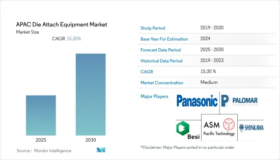
アジア太平洋のダイアタッチ装置市場は予測期間中にCAGR 15.3%を記録する見込み
主要ハイライト
- 市場ベンダーによる次の投資ラウンドの重要な焦点は、小型で非常に複雑な5G対応スマートフォン向けのダイボンディングとパッケージングソリューションの開発です。5Gは、将来の技術革新のための統一された接続プラットフォームであり、大幅に高速なデータとビデオ・トランスミッションで継続的なセキュアクラウドアクセスを可能にします。
- ユーザーが5G機能を採用することで、モバイルブロードバンド活動が拡大し、Internet of Everythingに向けた人工知能の利用が加速します。同様に、モバイルインターネット、コンピューティング、5G、車載エンドユーザー向けの基板とウエハーレベルパッケージングプロセスは、半導体産業のメモリとロジック向け設備投資の回復を牽引しました。
- 同社は、半導体とFPD用途の拡大に向けた中長期的な設備投資の増加計画を共有しています。一方、半導体組立装置では、FOWLP/PLPやμLED向けの高速・高精度ボンディング装置の積極的な開発が注目されます。
- BESIは、FOWLP、TCB、TSV、超薄型ダイ、ハイブリッドボンディング、大面積、ウエハーレベルモールド、ソーラー、3Dリチウムイオン電池めっきなど、新しいデジタル社会に対応した新しい組立技術への投資計画を共有しています。ダイアタッチ装置では、シングルチップ、マルチチップ、マルチモジュール、フリップチップ、TCB、FOWLP、ハイブリッドダイボンディングシステム、ダイソーティングシステムなどをラインアップしています。
- しかし、懸念材料としては、COVID-19の世界の蔓延の影響による先行き不透明感が続いていることです。COVID-19の発生によるアジア太平洋全域での操業停止と生産停止は、半導体の生産と消費に大きな影響を与えました。IDSと鋳造の大半がこの地域にあるため、操業停止の影響は設備投資への支出の減少につながりました。このことは、2021年にかけて回復が鈍化すると予想される市場調査に影響を与える可能性が高いです。
アジア太平洋ダイアタッチ装置市場動向
CISは大幅な成長が見込まれる
- CMOSイメージセンサは、スマートフォンやその他の製品にカメラ機能を提供してきたが、微細化需要が拡大するにつれて、ファブにおける製造上の問題が生じています。
- 3Gから4Gへ、現在は5Gへとデータ性能の広帯域化が進み、より高品質なカメラへの需要が高まっています。この動向は、より高い画素数と解像度の必要性によるCMOSイメージセンサの積層技術を推進してきました。こうした動向以外にも、バイオメトリクスID、3Dセンシング、強化された人間視覚用途のセグメントがセグメントの成長を拡大しています。
- より大きく、より優れたカメラに対する顧客の要求により、より大きなダイサイズのセンサが増えています。ピクセルスケーリング以外にも、CMOSイメージセンサはダイスタッキングのような技術革新が進んでいます。この市場のベンダーは、シリコン貫通電極(TSV)、ハイブリッドボンディング、ピクセル間ボンディングなど、さまざまな相互接続技術を使用しています。
- 例えば、ハイブリッドボンディングでは、ダイは銅と銅の相互接続で接続されます。このために、ファブでは2枚のウエハーが加工されます。1枚はロジックウエハーで、もう1枚はピクセルアレイウエハーです。2枚のウエハーは誘電体-誘電体接合で接合され、次に金属-金属接合で接合されます。
- Xperiの独自技術であるハイブリッド接合DBI技術は、Samsungの携帯電話用CMOSイメージセンサ製造に大きく利用されています。CMOSイメージセンサ向けのこの技術は、室温でのCu-Cu永久接合、低温アニール(約300℃)、外圧をかけない接合プロセス(誘電体/金属)を容易にします。
- これに先立ち、ダイレクトボンド技術は、15年以上にわたってXperiforが主導する複数の世代バリエーションを持つ画素スケーリング(裏面照射)BSIと積層BSIの実現において、実現可能な役割を果たしてきました。
シェアを独占するLED
- ダイアタッチ材料は、中・高・超高出力LEDの性能と信頼性に重要な役割を果たします。LED普及率の上昇に伴い、ダイアタッチ装置への需要が高まっています。特定のチップ構造と用途に適したダイアタッチ材料の選択は、パッケージングプロセス(スループットと歩留まり)、性能(放熱出力と光出力)、信頼性(ルーメン維持)、コストなど、さまざまな考慮事項によって決まります。LEDのダイアタッチには、共晶金錫、銀入りエポキシ、はんだ、シリコーン、焼結材料などが使用されてきました。
- SFEは、LEDエポキシダイボンダーマシンのインデックスタイム0.2秒/サイクル(動作率90%)、チップサイズ250*250規格、2台のカメラによるリードフレーム認識を提供するエポキシ接着剤ボンディング方式を提供しています。そのソフトウェア機能は、自動マウントレベルとピックアップレベルのティーチング機能を記載しています。
- さらに、導電性接着剤(主に銀充填エポキシ)は、LED用熱ダイアタッチ材料の最大クラス(個数ベース)を構成しています。これらは、既存のバックエンドパッケージング装置と互換性があり、魅力的なコスト・パフォーマンス・バランス(通常、二次リフロー互換で最大50W/mKの熱)を記載しています。ベアシリコンに固着するため、GaN on Siliconのようなバックエンドのメタライゼーションのないダイに最も好まれる材料です。
- さらに、LED市場には多くの競合他社が存在するが、ASMはこの市場における著名な参入企業の1つであり、同社のLEDエポキシ高速ダイボンダーAD830はLED市場を独占しています。高速、高信頼性、高精度で、ダイの配置精度は+/-1mil、+/-3度、10mil x 10milのような小型チップのサイクルタイムは180msで、これは1万8,000UPHに相当します。あらかじめ設定された配置範囲でボンディングされたユニットをモニタリングするポストボンド検査システムが装備されています。
アジア太平洋ダイアタッチ装置産業概要
アジア太平洋のダイアタッチ装置市場は中程度の競争であり、多数の企業が小さな市場シェアを有しています。各社は市場シェアを維持するために技術革新を続け、戦略的パートナーシップを結んでいます。
- 2022年4月-Electric Revolution Industrialization Centre(DER-IC)North Eastは、パワーエレクトロニクス、機械、ドライブ(PEMD)能力を向上させるため、工具・材料のトップ技術ディストリビューターであるInsetoから設備を受領しました。英国で初めて導入されるマイクロパンチマシンはAMX P100シンタープレスで、提供される設備の一部であり、高信頼性、高出力モジュールの生産を可能にします。
- 2022年6月-West Bondが新しい7KFボンダーシリーズを開発しました。この有名な会社は、マイクロエレクトロニクスパッケージング産業向けに、ワイヤボンディング機、ダイトゥアタッチ機、ワイヤ引張検査機、せん断検査機、超音波部品、付属品の製品ラインを設計・製造しています。この優れたツールは、RF、マイクロ波、半導体、ハイブリッド、医療機器セグメントで見られる困難なボンディング用途を処理するために作られています。
その他の特典
- エクセル形式の市場予測(ME)シート
- 3ヶ月のアナリストサポート
目次
第1章 イントロダクション
- 調査の前提条件と市場定義
- 調査範囲
第2章 調査手法
第3章 エグゼクティブサマリー
第4章 市場力学
- 市場概要
- 産業の魅力-ポーターのファイブフォース分析
- 供給企業の交渉力
- 買い手の交渉力
- 新規参入業者の脅威
- 代替品の脅威
- 競争企業間の敵対関係
- 産業バリューチェーン分析
- COVID-19が市場に与える影響
第5章 市場促進要因
- AuSn共晶ダイアタッチ技術の需要拡大
- ディスクリートパワーデバイスの需要
第6章 市場課題
- 加工・寿命中の寸法変化と機械的アンバランス
第7章 市場セグメンテーション
- ボンディング技術
- ダイボンダー
- エポキシ/接着剤(ペースト/フィルム)
- 共晶
- はんだ
- 焼結
- フリップチップボンダー
- ピックアンドプレイス/リフローはんだ付け
- サーモコンプレッション(TCB)
- サーモソニックボンディング
- ハイブリッドボンディング
- ダイボンダー
- 用途
- メモリー
- LED
- ロジック
- CMOSイメージセンサ
- オプトエレクトロニクス/フォトニクス
- ディスクリートパワーデバイス
- MEMS&センサ
- 積層メモリー&RF
- 国名
- 台湾
- 中国
- 日本
- 韓国
- 東南アジア
第8章 競合情勢
- 企業プロファイル
- Palomar Technologies, Inc.
- Shinkawa Ltd
- Panasonic Corporation
- ASM Pacific Technology Limited
- Be Semiconductor Industries NV(Besi)
- Shibaura Mechatronics Corporation
- ficonTEC Trading Ltd(ficonTEC Service GmbH)
- Fasford Technology Co Ltd.
- Dongguan Hoson Electronic Technology Ltd
- For Technos Co., Ltd.
- Shenzhen Xinyichang Technology Co., Ltd.(Hoson)
第9章 ベンダーの市場シェア分析~2021年
第10章 投資分析
第11章 投資分析市場の将来
目次
Product Code: 71756
The APAC Die Attach Equipment Market is expected to register a CAGR of 15.3% during the forecast period.
Key Highlights
- A significant focus for the next investment round by market vendors is developing die bonding and packaging solutions for smaller and highly complex 5G compatible smartphones. 5G is a unifying connectivity platform for future innovation, enabling continuous secure cloud access at significantly higher data and video transmission speeds.
- User adoption of 5G capabilities expands mobile broadband activities and accelerates artificial intelligence usage for the Internet of Everything. Likewise, the substrate and wafer-level packaging processes for mobile internet, computing, 5G, and automotive end-user applications drove the semiconductor industry to see a recovery in capital investment for memories and logic.
- The company has shared plans for a medium-to-long-term increase in capital investment towards expanded semiconductor and FPD applications. Whereas, as per Shibaura, active development of high-speed, high-precision bonding equipment for FOWLP / PLP and μLED is being looked out for in semiconductor assembly equipment.
- BESI has shared plans to invest in new assembly technologies such as FOWLP, TCB, TSV, ultra-thin dies, hybrid bonding, large area, wafer level molding, solar, and 3D-lithium-ion battery plating for the new digital society. Its lineup under Die attach equipment includes a single chip, multi-chip, multi-module, flip chip, TCB, FOWLP, hybrid die bonding systems, and die sorting systems.
- However, one source of concern is the continuing uncertain outlook due to the impact of the global spread of COVID-19. Lockdowns and production halts across Asia-pacific due to the COVID-19 outbreak had significantly impacted the production and consumption of semiconductors. With the majority of the IDS and foundries located in the region, the impact of shutdowns has led to reduced spending on capital investments. This is likely to impact the market studied, with a slowed recovery expected across 2021.
APAC Die Attach Equipment Market Trends
CIS is expected to witness significant growth
- CMOS image sensors have been offering camera functions in smartphones and other products, and as the scaling demand grows, the related manufacturing issues in the fab arise.
- The higher-bandwidth data performance progressed from 3G to 4G, and currently, to 5G, the demand for higher quality cameras has grown. This trend has propelled the CMOS image sensor stacking techniques based on the need for higher pixel counts and better resolution. Beyond these trends, the areas of biometric ID, 3D sensing, and enhanced human vision applications have augmented segment growth.
- Customer demand for bigger and better cameras results in more sensors with bigger die sizes. Besides pixel scaling, CMOS image sensors are undergoing other innovations like die stacking. Vendors in the market studied are also using different interconnect technologies, such as through-silicon vias (TSVs), hybrid bonding, and pixel-to-pixel for the same.
- In hybrid bonding, for instance, the dies are connected using copper-to-copper interconnects. For this, two wafers are processed in a fab. One is the logic wafer, while the other is the pixel array wafer. The two wafers are joined using a dielectric-to-dielectric bond, followed by a metal-to-metal connection.
- Hybrid bonding DBI technologies, Xperi'sproprietary technology, are being significantly used by Samsung towards CMOS image sensor fabrication for its phones. This technology for CMOS Image Sensors facilitates room temperature Cu-Cu permanent bonding, low-temperature annealing (around 300°C) & no external pressure bonding process (dielectric/metal).
- Prior to this, direct bond technology has thus played an enabling role in the realization of pixel scaling (backside illumination) BSI and stacked BSI with multiple generational variations led by Xperifor over 15 years.
LED to dominate market share
- Die attach material represents a key role in the performance and reliability of mid, high, and super-high power LEDs. The demand for die-attach equipment is increasing with an increasing LED penetration rate. The selection of suitable die-attach material for a particular chip structure and application depends on various considerations, which include the packaging process (throughput and yield), performance (thermal dissipation output and light output), reliability (lumen maintenance), and cost. Eutectic gold-tin, silver-filled epoxies, solder, silicones, and sintered materials have all been used for LED die attach.
- SFE provides an Epoxy Adhesive bonding method where its LED Epoxy Die Bonder machine features an index time of 0.2 Sec /Cycle (90 Percent Rate of Operation) with a chip size of 250 * 250 standards, providing lead frame recognition through 2 Cameras. Its software function provides auto mount level & pick up level teaching functions.
- Further, conductive adhesives (mostly silver-filled epoxies) constitute the largest class of thermal die-attach materials (by unit number) for LEDs. They are compatible with existing back-end packaging equipment and provide an attractive cost/performance balance (typically up to 50 W/mK thermals with secondary reflow compatibility). As they stick to bare silicon, they are the most preferred material for dies without back-end metallization like GaN on silicon.
- Further, in the LED market, there are a lot of rival competitors, and ASM is one of the prominent players in this market; its LED Epoxy High speed die bonder AD830 dominates in the LED market. It is fast, reliable, and accurate with die placement accuracy of +/-1 mil and +/-3 degree, cycle time for a small chip like 10mil x 10mil is 180 ms, which is an equivalent UPH of 18,000. It is equipped with a Post bond inspection system that monitors the bonded unit at the pre-set placement range.
APAC Die Attach Equipment Industry Overview
The APAC Die attach equipment market is moderately competitive, with a large number of players having a small market share. The companies keep innovating and entering into strategic partnerships to maintain their market share.
- April 2022 - Driving the Electric Revolution Industrialization Centre (DER-IC) North East has received equipment from Inseto, a top technical distributor of tools and materials, to improve its power electronics, machines, and drives (PEMD) capabilities. The first micro-punch machine to be installed in the UK is an AMX P100 sinter press, which is part of the equipment provided and will allow the production of high-reliability, high-power modules.
- June 2022 - The new 7KF Bonder Series has been developed by West Bond. This well-known company designs and manufactures a line of wire bonding and die-to-attach machines, wire pull and shear test equipment, ultrasonic components, and accessories for the microelectronics packaging industry. This excellent tool is made to handle the difficult bonding applications found in the RF, microwave, semiconductor, hybrid, and medical device fields.
Additional Benefits:
- The market estimate (ME) sheet in Excel format
- 3 months of analyst support
TABLE OF CONTENTS
1 INTRODUCTION
- 1.1 Study Assumptions and Market Definition
- 1.2 Scope of the Study
2 RESEARCH METHODOLOGY
3 EXECUTIVE SUMMARY
4 MARKET DYNAMICS
- 4.1 Market Overview
- 4.2 Industry Attractiveness - Porter's Five Forces Analysis
- 4.2.1 Bargaining Power of Suppliers
- 4.2.2 Bargaining Power of Buyers
- 4.2.3 Threat of New Entrants
- 4.2.4 Threat of Substitutes
- 4.2.5 Intensity of Competitive Rivalry
- 4.3 Industry Value Chain Analysis
- 4.4 Impact of Covid-19 on the market
5 Market Drivers
- 5.1 Growing Demand of AuSn Eutectic Die-Attach Technology
- 5.2 Demand of Discrete Power Devices
6 Market Challenges
- 6.1 Dimensional Changes During Processing and Service Life and Mechanical Unbalance
7 MARKET SEGMENTATION
- 7.1 By Bonding Technique
- 7.1.1 Die Bonder
- 7.1.1.1 Epoxy/Adhesive (paste/film)
- 7.1.1.2 Eutectic
- 7.1.1.3 Solder
- 7.1.1.4 Sintering
- 7.1.2 Flip Chip Bonder
- 7.1.2.1 Pick and Place / reflow soldering
- 7.1.2.2 Thermocompresion (TCB)
- 7.1.2.3 Thermosonic Bonding
- 7.1.2.4 Hybrid Bonding
- 7.1.1 Die Bonder
- 7.2 Application
- 7.2.1 Memory
- 7.2.2 LED
- 7.2.3 Logic
- 7.2.4 CMOS Image Sensor
- 7.2.5 Optoelectronics / Photonics
- 7.2.6 Discrete Power Devices
- 7.2.7 MEMS & Sensors
- 7.2.8 Stacked Memory & RF
- 7.3 Country
- 7.3.1 Taiwan
- 7.3.2 China
- 7.3.3 Japan
- 7.3.4 Korea
- 7.3.5 Southeast Asia
8 COMPETITIVE LANDSCAPE
- 8.1 Company Profiles
- 8.1.1 Palomar Technologies, Inc.
- 8.1.2 Shinkawa Ltd
- 8.1.3 Panasonic Corporation
- 8.1.4 ASM Pacific Technology Limited
- 8.1.5 Be Semiconductor Industries NV (Besi)
- 8.1.6 Shibaura Mechatronics Corporation
- 8.1.7 ficonTEC Trading Ltd (ficonTEC Service GmbH)
- 8.1.8 Fasford Technology Co Ltd.
- 8.1.9 Dongguan Hoson Electronic Technology Ltd
- 8.1.10 For Technos Co., Ltd.
- 8.1.11 Shenzhen Xinyichang Technology Co., Ltd. (Hoson)
9 VENDOR MARKET SHARE ANALYSIS - 2021
10 INVESTMENT ANALYSIS
11 FUTURE OF THE MARKET
アジア太平洋のダイアタッチ装置:市場シェア分析、産業動向、成長予測(2025~2030年)
- 発行日
- 発行
- Mordor Intelligence
- ページ情報
- 英文 120 Pages
- 納期
- 2~3営業日