
|
市場調査レポート
商品コード
1692440
半導体フロントエンド装置:市場シェア分析、産業動向・統計、成長予測(2025年~2030年)Semiconductor Front End Equipment - Market Share Analysis, Industry Trends & Statistics, Growth Forecasts (2025 - 2030) |
||||||
カスタマイズ可能
適宜更新あり
|
|||||||
| 半導体フロントエンド装置:市場シェア分析、産業動向・統計、成長予測(2025年~2030年) |
|
出版日: 2025年03月18日
発行: Mordor Intelligence
ページ情報: 英文 148 Pages
納期: 2~3営業日
|

全表示
- 概要
- 目次
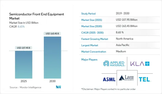
半導体フロントエンド装置市場規模は、2025年に1,079億5,000万米ドルと推定され、2030年には1,634億5,000万米ドルに達すると予測され、予測期間(2025年~2030年)のCAGRは8.65%です。
前工程では、ウエハーを完成したデバイスに変換するために多くの複雑な段階が必要となります。これらの段階には、ウエハーの洗浄、酸化、デバイスをパターン化するフォトリソグラフィー、エッチング、蒸着、ドーピング、メタライゼーションなどのステップが含まれます。工程管理には、検査・計測装置が利用されます。これは、最終製品に問題を引き起こす可能性のある不規則性を特定するためにウエハーを検査するものです。これに加えて、光学技術も使用され、微小な欠陥を見つけるために電子ビーム検査が必要になることも多いです。
主なハイライト
- 半導体フロントエンド装置の需要は、主要な前工程装置メーカーが半導体業界の低迷を背景に記録的な収益を達成したことから、短期的な調整ではなく、顕著な急増が見込まれます。これは、生産能力の拡大、新しい工場プロジェクト、そして前工程装置市場全体の先端技術とソリューションに対する高い需要が原動力となっています。
- 昨年、大幅な売上高を記録したウエハー処理装置、ファブ設備、マスク・レチクル装置を含むウエハー製造装置は、2023年にはやや低水準になると予測されており、今回の縮小は大幅な改善を意味します。今回の上方修正は、主に中国の好調な設備投資によるものです。市場は、米国やオランダ政府の輸出管理規制を含む地政学的課題や、インフレ、金利上昇、特定経済圏のGDP成長率低下をめぐる世界のマクロ懸念によって生じた不確実性を管理しながら成長しました。
- 民生用電子機器が最も急成長している分野であり、市場拡大に寄与しています。人口増加に伴い増加すると予想されるスマートフォンの利用が、この市場の主な促進要因です。タブレット、スマートフォン、ノートパソコン、パソコン、ウェアラブルガジェットなどの需要増加により、コンシューマーエレクトロニクスが業界を牽引しています。半導体の進歩に伴い、機械学習などの新たな市場分野が急速に統合されつつあります。
- 人工知能、モノのインターネット、量子コンピューティング、強化されたワイヤレスネットワークなど、未来の最も魅力的な「必勝」技術は現在、半導体によって支えられています。半導体とマイクロエレクトロニクスは、世界が画期的な技術を生活のあらゆる側面にシームレスに統合する中で、絶えず変化するデジタル環境の複雑な要求を満たすために進歩しています。ビッグデータとAIがこの増加を後押しし、より小型で強力なチップを要求しているため、その製造はより困難となり、技術革新の必要性が高まっています。
- データストレージ、計算能力、アルゴリズムの急速な進歩により、AIシステムの開発と展開が可能になりました。デジタル機器やインターネットの利用が増えたことで、大量のデータが生成されるようになりました。AIシステムは、学習と性能向上のために大規模なデータセットに依存しています。
- モノのインターネット(IoT)、ビッグデータ、クラウド・マニュファクチャリング、サイバー・フィジカル・システム(CPS)、サービスのインターネット(IoS)、ロボット工学、拡張現実(AR)、その他の新興技術は、インダストリー4.0の考えに含まれています。さらなるスマートな産業プロセスを生み出すには、これらの技術を採用することが重要であり、それは将来の産業の進歩をいくつか包含することで、物理的な世界とデジタルの世界を統合することになります。
- 世界の在宅勤務の動向が勢いを増すにつれ、クラウド・サービスへの需要が急増し、データセンター・プロバイダーはその能力を拡大する必要に迫られます。その結果、チップとメモリに対する世界の需要が高まる。SEMIは、300mmファブへの投資が顕著に増加していると報告しています。予測によると、業界では2020年から2024年の間に最低でも38の300mmファブが新設されます。
- この急増により、ウエハー生産能力は約180万枚増加し、合計で700万枚を超えることになります。注目すべきは、台湾がこのうち11カ所の新しい量産工場を建設する予定で、中国が8カ所でこれに続くことです。さらに、TSMCはアリゾナに新しい300mmファブを建設中です。2024年末までには、300mm量産工場は161カ所に達すると予想されます。
半導体フロントエンド装置市場動向
半導体製造工場が最大のエンドユーザー産業に
- 設計段階の後、半導体チップはファブや鋳造と呼ばれる施設で製造されます。フロントエンド・ファブリケーションでは、チップはウェハーと呼ばれるシリコンの円形シート、またはあまり一般的でない他の半導体材料の上に製造されます。
- ファブリケーションは、様々な中小企業と材料に依存して、設計をチップに変えるプロセスです。まず、炉でシリコンの円柱を形成し、それを円盤状のウェハーに切断します。半導体製造施設(「ファブ」)は、シリコン内の材料層にトランジスタやその他の電気デバイスを形成し、シリコンの上の絶縁層に電気デバイス間の金属相互接続を形成するという2つのステップでチップをウエハーにします。電気デバイスと相互接続が組み合わさって回路が形成されます。
- 米国、台湾、韓国、日本、中国に本社を置く企業が、世界の半導体製造工場の市場シェアと製造能力の大半を支配しており、これらの企業は物理的にもこれらの国に位置しています。半導体製品の開発には、(材料から物流に至るまで)多くのビジネスが調和して働くことが必要です。半導体デバイスの製造工程が複雑なため、開発コストも増大しています。企業はさまざまなビジネスモデルを活用することで、出費を抑え、半導体で生き残りを図ってきました。
- 2023年11月、中国は8億1,680万米ドルに相当する42台のリソグラフィ・システムを持ち込みました。オランダは16台のリソグラフィ・システムを供給し、総額は7億6,270万米ドルで、前年から10倍に増加しました。さらに、中国は10月にオランダから21台のシステムを輸入しました。日本のキヤノンとニコンも中国に露光装置を供給しました。このように、半導体製造工場における前工程装置の需要は上方修正が予想されます。
- 世界経済の回復が見込まれ、来年のスマートフォン、サーバー、ノートパソコン、テレビ、自動車市場の成長だけでなく、5G基地局やWi-Fi 6技術を含む次世代ネットワークの継続的な展開により、部品需要の増加が予想されます。
- European 5G Observatoryによると、2023年時点で、ドイツは欧州連合(EU)加盟国の中で最大の5G基地局を有し、約9万基地局が設置されています。これらのチップの設計・製造とその研究は、何十万もの高賃金の雇用を提供できるため、オンショアリング/リショアリングは政治的に人気のある話題となっています。そのため、鋳造所や装置メーカーは、それぞれのバックヤードで莫大な投資を計画し、マッピングしています。例えば、東京エレクトロンは、日本における装置製造設備に6億米ドル以上を投資する計画を発表しました。
- IDMはウエハー製造能力に投資することで、依然として重要な役割を果たしています。例えば、2023年6月、インテルとドイツ政府は、マグデブルクに300億ユーロ以上の最先端ウエハー製造拠点を計画するための修正趣意書に署名し、2つの欧州初の半導体施設を建設すると発表しました。韓国メディアによると、同社は2023年12月、ASMLから高NAのEUV露光装置6台を取得し、2024年に出荷する予定と報じられています。この買収は、2nmノードでサムスンやTSMCを追い抜くための秘密兵器になるとみられています。
- 2023年7月、サムスンはテキサス州オースティンの1,200エーカーの土地に170億米ドルを投じて半導体製造工場を建設すると発表しました。中国と台湾間の地政学的緊張のため、チップメーカーは米国に製造拠点を求めました。税金が安く、新たな補助金もあるため、テキサスはビジネスを行うのに適した場所として浮上しました。世界の半導体製造装置メーカーは韓国で施設を拡張しています。新たな国内生産拠点に今後20年間で2,300億米ドルを投資する計画で、他の企業を引き付け、チップ供給体制を育成しています。
中国が大きな市場シェアを占める見込み
- CSETによると、中国は組立・パッケージングツール以外のすべての主要セグメントで注目すべき市場シェアを占めています。しかし、リソグラフィ装置、特に極端紫外線(EUV)フォトリソグラフィと深紫外線(DUV)フォトリソグラフィでは、中国は最大の課題に直面しています。
- インプリントリソグラフィ、電子ビーム、レーザーリソグラフィ、レジスト処理装置、フォトマスク検査、リペアツールなどが大きな障害となっています。過去数年間、中国はチップ産業を支えるため、先進的なリソグラフィ装置の輸入に一貫して投資してきました。
- しかし、その技術力を背景に、中国は常に前工程装置への依存度を高め、それを市場に導入するために大規模な投資を行っています。
- 2023年12月、中国のリソグラフィ装置専門企業である上海微電子設備集団(SMEE)は、28nmクラスの最先端プロセス技術でウエハー加工が可能な初号機を発表しました。この重要な成果は、SMEEの先進的なリソグラフィ装置構築への献身を浮き彫りにするものです。同装置はSSA/800-10Wと呼ばれ、同社にとって重要なマイルストーンとなります。
- 米国の制裁措置は、日中間の技術的な対立が激化する中、世界的に最先端のチップを開発する中国の進歩を妨げるために策定されました。SMICと他のチップ・メーカーは、チップ生産を進めることで国家の自主性を高めることに専念しています。SMICは、先進的なリソグラフィ装置を活用し、現地の装置メーカーと緊密に協力し、先端ノード・プロセスの歩留まりを高めるためにファーウェイに外部支援を求めています。
- 米国による中国技術への制裁が続いているため、この地域は自給自足に努めています。中国政府は先端チップ技術の研究開発に多額の投資を行っています。また、経済や電気自動車(EV)のような新興産業でさまざまな用途に使われる高ノードチップに重点を移すよう、地元メーカーを奨励しています。政府のイニシアチブの高まりと、国内チップ生産を強化するための地元ベンダーによる投資の増加は、フロントエンド市場に注目すべき需要を生み出すと予想されます。
- CAAMによると、2023年8月の中国の新エネルギー車販売台数は約84万6,000台で、うち80万8,000台が乗用電気自動車、3万9,000台が商用電気自動車でした。乗用バッテリー電気自動車(BEV)は55.9万台、乗用プラグインハイブリッド電気自動車(PHEV)は24.8万台でした。
半導体フロントエンド装置市場概要
半導体フロントエンド装置市場は、Applied Materials Inc.市場各社は、製品ラインナップを強化し、持続的な競争優位性を獲得するために、パートナーシップ、イノベーション、買収などの戦略を採用しています。
- 2024年2月-ASML Holding NVは、エアバスA320型機2機分の重量を持つ、価格3億5,000万ユーロの最新チップ製造機「High-NA」を発表。インテル社は、オレゴン工場への初出荷を確保し、チップ生産は来年後半に開始される予定。同機は8ナノメートル厚の半導体ラインを実現し、従来の1.7倍に縮小、チップのトランジスタ密度を高めて処理速度とメモリを向上させる。
- 2024年1月- アプライドマテリアルズがグーグルと提携し、拡張現実(AR)技術を推進。この提携は、アプライドマテリアルズの材料工学の専門知識とグーグルのプラットフォームを活用し、次世代のAR体験のための軽量ビジュアルディスプレイシステムを開発するものです。その目的は、複数世代のAR製品、アプリケーション、サービスの開発を加速することです。
その他の特典
- エクセル形式の市場予測(ME)シート
- 3ヶ月間のアナリストサポート
目次
第1章 イントロダクション
- 調査の前提条件と市場定義
- 調査範囲
第2章 調査手法
第3章 エグゼクティブサマリー
第4章 市場洞察
- 市場概要
- 業界の魅力度-ポーターのファイブフォース分析
- 供給企業の交渉力
- 買い手の交渉力
- 新規参入業者の脅威
- 代替品の脅威
- 競合の度合い
- 業界バリューチェーン分析
- COVID-19パンデミックの市場への影響
第5章 市場力学
- 市場促進要因
- 民生用電子機器へのニーズの高まりが製造業の見通しを押し上げる
- 業界別人工知能、IoT、コネクテッドデバイスの普及
- 市場抑制要因
- 技術のダイナミックな性質により、製造設備に数回の変更が必要
第6章 市場セグメンテーション
- タイプ別
- リソグラフィー装置
- エッチング装置
- 蒸着装置
- その他の装置タイプ
- エンドユーザー産業別
- 半導体製造工場
- 半導体エレクトロニクス製造
- 地域別
- 米国
- 欧州
- 中国
- 韓国
- 台湾
- 日本
- ラテンアメリカ
- 中東・アフリカ
第7章 競合情勢
- 企業プロファイル
- Applied Materials Inc.
- ASML Holding NV
- Tokyo Electron Limited
- LAM Research Corporation
- KLA Corporation
- Nikon Corporation
- VEECO Instruments Inc.
- Plasma Therm
- Hitachi High-Technologies Corporation
- Carl Zeiss AG
- Screen Holdings Co. Ltd
第8章 投資分析
第9章 市場の将来
The Semiconductor Front End Equipment Market size is estimated at USD 107.95 billion in 2025, and is expected to reach USD 163.45 billion by 2030, at a CAGR of 8.65% during the forecast period (2025-2030).
The front-end procedure necessitates a multitude of intricate phases to convert a wafer into a completed device. These steps incorporate wafer cleaning, oxidation, and photolithography to pattern devices, along with etching, deposition, doping, and metallization steps. Inspection and metrology equipment is utilized for process control. This is when the wafers are inspected to identify irregularities that potentially induce issues with the end product. In addition to this, optical techniques are also used, and e-beam inspection is often needed to find the smallest defects.
Key Highlights
- The demand for semiconductor front-end equipment is expected to observe a noteworthy surge as some of the major front-end equipment-producing companies observed record-breaking revenue against a backdrop of a downturn in the semiconductor industry instead of the mild and short-term correction. It was driven by capacity expansion, new fab projects, and high demand for advanced technologies and solutions across the front-end equipment market.
- After registering a record of significant sales last year, the wafer fab equipment, which includes wafer processing, fab facilities, and mask/reticle equipment, is projected to be a bit low in 2023, and this contraction marks a significant improvement. The upward revision is primarily due to China's strong equipment spending. The market grew managing uncertainties created by geopolitical challenges, including the US and Dutch governments' export control regulations and global macro concerns around inflation, rising interest rates, and lower GDP growth in certain economies.
- Consumer electronics is the fastest-growing segment, contributing to market expansion. The use of smartphones, anticipated to rise with population growth, is the key driver of this market. Consumer electronics drive the industry due to increased demand for tablets, smartphones, laptops, computers, and wearable gadgets. As semiconductors advance, new market areas, such as machine learning, are rapidly being integrated.
- The most fascinating "must-win" technologies of the future, such as artificial intelligence, the Internet of Things, quantum computing, and enhanced wireless networks, are currently supported by semiconductors. Semiconductors and microelectronics are advancing to satisfy the complicated demands of a constantly changing digital environment as the world seamlessly integrates breakthrough technology into every aspect of life. Big Data and AI drive this increase and call for smaller, more powerful chips, making their production more difficult and increasing the need for technological innovation.
- Rapid advancements in data storage, computing power, and algorithms have enabled the development and deployment of AI systems. The increased use of digital devices and the Internet has generated extensive volumes of data. AI systems rely on large datasets to train and improve their performance.
- The Internet of Things (IoT), big data, cloud manufacturing, cyber-physical systems (CPS), the Internet of Services (IoS), robotics, augmented reality, and other emerging technologies are included in the Industry 4.0 idea. Creating additional smart industrial processes depends on adopting these technologies, which will unite the physical and digital worlds by encompassing several future industrial advancements.
- As global work-from-home trends gain momentum, the demand for cloud services surges, prompting data center providers to expand their capacities. This, in turn, fuels the global appetite for chips and memory. SEMI reports a notable uptick in investments in 300 mm fabs. Projections suggest that the industry will witness the addition of a minimum of 38 new 300 mm fabs between 2020 and 2024.
- This surge is set to boost the capacity by approximately 1.8 million wafers, pushing the total beyond 7 million. Notably, Taiwan is slated to host 11 of these new volume fabs, with China following closely with eight. Additionally, TSMC is in the process of constructing a new 300 mm fab in Arizona. By the close of 2024, the tally of 300 mm volume fabs is anticipated to hit a significant 161 units.
Semiconductor Front End Equipment Market Trends
Semiconductor Fabrication Plant to be the Largest End-user Industry
- After the design stage, semiconductor chips are manufactured or fabricated in facilities called fabs or foundries. In front-end fabrication, chips are manufactured on circular sheets of silicon or, less commonly, other semiconducting materials called wafers, typically about 8 or 12 inches in diameter.
- Fabrication is a process that turns designs into chips, relying on various SMEs and materials. First, a furnace forms a cylinder of silicon, which is cut into disc-shaped wafers. Semiconductor fabrication facilities ("fabs") make chips into wafers in two steps: forming transistors and other electrical devices in material layers within the silicon and forming metal interconnects between the electrical devices in insulating layers above the silicon. Together, the electrical devices and interconnects form circuits.
- Firms headquartered in the United States, Taiwan, South Korea, Japan, and China control most of the world's fab market share and fab capacity, which are also physically located in these countries. Semiconductor product development requires working harmoniously for many businesses (from materials to logistics). The complex process of fabricating semiconductor devices has also increased the development cost. Companies have leveraged different business models to lower expenditures and survive in semiconductors.
- In November 2023, China brought 42 lithography systems worth USD 816.8 million. The Netherlands supplied 16 lithography systems, totaling USD 762.7 million, a tenfold increase from the previous year. Additionally, China imported 21 systems from the Netherlands in October. Japanese companies Canon and Nikon also supplied China with lithography tools. Thus, an upward revision is expected in the demand for front-end equipment in semiconductor fabrication plants.
- The global economy is expected to recover, and the demand for components is expected to rise owing to not only growth in the smartphone, server, notebook computer, TV, and automobile markets next year but also the continued rollout of next-generation networks, including 5G base stations and Wi-Fi 6 technologies.
- According to the European 5G Observatory, as of 2023, Germany had the maximum 5G base stations among European Union (EU) member states, with approximately 90,000 base stations installed. The design and manufacturing of these chips and their research can provide hundreds of thousands of high-paying jobs, making onshoring/re-shoring a popular topic politically. It is why foundries and equipment companies are planning and mapping enormous investments in their backyards. For instance, TEL announced plans to invest more than USD 600 million in equipment manufacturing facilities in Japan.
- IDMs still play a significant role by investing in wafer fabrication capacities. For instance, in June 2023, Intel and the German government announced signing a revised letter of intent for planning a leading-edge wafer fabrication site in Magdeburg with more than EUR 30 billion for two first-of-a-kind European semiconductor facilities. In December 2023, the company reportedly acquired six high-NA EUV lithography machines from ASML, which is scheduled for shipment in 2024, according to South Korean media outlets. This acquisition is expected to be its secret weapon to overtake Samsung and TSMC at the 2nm node.
- In July 2023, Samsung announced it would spend USD 17 billion to build a semiconductor fabrication plant on a 1,200-acre plot of land in Austin, Texas. Owing to the geopolitical tension between China and Taiwan, chipmakers turned to the United States for manufacturing. Due to low taxes and new subsidies, Texas has emerged as a suitable place to do business. Global semiconductor manufacturing equipment companies are expanding facilities in South Korea. The company plans to invest USD 230 billion over the next 20 years in a new domestic production hub, attracting other players and fostering a chip supply system.
China is Expected to Hold a Significant Market Share
- According to CSET, China holds a noteworthy market share in all major segments besides assembly and packaging tools. However, China faces the greatest challenge in lithography tools, particularly extreme ultraviolet (EUV) photolithography and deep ultraviolet (DUV) photolithography.
- Imprint lithography, e-beam, laser lithography, resist processing equipment, photomask inspection, and repair tools pose significant obstacles. Over the past few years, China has consistently invested in importing advanced lithography equipment to support its chip industry.
- However, with its technological capabilities, the country constantly strives to enhance its self-dependency on front-end equipment and invest significantly to introduce it into the market.
- In December 2023, Shanghai Micro Electronics Equipment Group (SMEE), a Chinese company specializing in lithography tools, unveiled its inaugural machine capable of processing wafers using a cutting-edge 28nm-class process technology. This significant achievement highlights SMEE's dedication to constructing advanced lithography machines. The scanner, known as SSA/800-10W, marks a significant milestone for the company.
- US sanctions have been formulated to impede China's progress in developing the most cutting-edge chips globally as the technological rivalry between the two countries intensifies. SMIC and other chip manufacturers are dedicated to enhancing the nation's autonomy by advancing chip production. SMIC collaborates closely with local tool manufacturers, utilizing its advanced lithography equipment, and seeks external assistance from Huawei to enhance yields in advanced node processes.
- Due to the continuous US sanctions on Chinese technology, the area strives for self-sufficiency. The Chinese government is investing substantially in the research and development of advanced chip technology. It also encourages local manufacturers to shift their focus to higher-node chips with various uses in the economy and emerging industries like electric vehicles (EVs). The growing government initiatives and the increasing investments by local vendors to boost domestic chip production are expected to create a notable demand for the front-end market.
- According to CAAM, in August 2023, China's new energy vehicle sales were approximately 846,000 units, of which 808,000 were passenger electric vehicles and 39,000 were commercial electric vehicles. The sales of passenger battery electric vehicles (BEVs) and passenger plug-in hybrid electric vehicles (PHEVs) were 559,000 and 248,000 units, respectively.
Semiconductor Front End Equipment Market Overview
The semiconductor front-end equipment market is semi-consolidated, with major players like Applied Materials Inc., ASML Holding NV, Tokyo Electron Limited, LAM Research Corporation, and KLA Corporation. Market players are adopting strategies such as partnerships, innovations, and acquisitions to enhance their product offerings and gain sustainable competitive advantage.
- February 2024 - ASML Holding NV unveiled its latest chipmaking machine, the High-NA extreme ultraviolet, priced at EUR 350 million, weighing as much as two Airbus A320s. Intel Corp. secured the first shipment for its Oregon factory, with chip production set to begin late next year. The machine achieves 8-nanometer thick semiconductor lines, 1.7 times smaller than its predecessor, enhancing chip transistor density for increased processing speeds and memory.
- January 2024 - Applied Materials Inc. collaborated with Google to advance augmented reality (AR) technologies. This partnership leverages Applied Materials' expertise in materials engineering with Google's platforms to develop lightweight visual display systems for the next era of AR experiences. The goal is to expedite the creation of multiple generations of AR products, applications, and services.
Additional Benefits:
- The market estimate (ME) sheet in Excel format
- 3 months of analyst support
TABLE OF CONTENTS
1 INTRODUCTION
- 1.1 Study Assumptions and Market Definition
- 1.2 Scope of the Study
2 RESEARCH METHODOLOGY
3 EXECUTIVE SUMMARY
4 MARKET INSIGHTS
- 4.1 Market Overview
- 4.2 Industry Attractiveness - Porter's Five Forces Analysis
- 4.2.1 Bargaining Power of Suppliers
- 4.2.2 Bargaining Power of Buyers
- 4.2.3 Threat of New Entrants
- 4.2.4 Threat of Substitute Products
- 4.2.5 Degree of Competition
- 4.3 Industry Value Chain Analysis
- 4.4 Impact of COVID-19 Pandemic on the Market
5 MARKET DYNAMICS
- 5.1 Market Drivers
- 5.1.1 Increasing Needs of Consumer Electronic Devices Boosting the Manufacturing Prospects
- 5.1.2 Proliferation of Artificial Intelligence, IoT, and Connected Devices Across Industry Verticals
- 5.2 Market Restraints
- 5.2.1 Dynamic Nature of Technologies Requires Several Changes in Manufacturing Equipment
6 MARKET SEGMENTATION
- 6.1 By Type
- 6.1.1 Lithography Equipment
- 6.1.2 Etching Equipment
- 6.1.3 Deposition Equipment
- 6.1.4 Other Equipment Types
- 6.2 By End-user Industry
- 6.2.1 Semiconductor Fabrication Plant
- 6.2.2 Semiconductor Electronics Manufacturing
- 6.3 By Geography
- 6.3.1 United States
- 6.3.2 Europe
- 6.3.3 China
- 6.3.4 South Korea
- 6.3.5 Taiwan
- 6.3.6 Japan
- 6.3.7 Latin America
- 6.3.8 Middle East and Africa
7 COMPETITIVE LANDSCAPE
- 7.1 Company Profiles
- 7.1.1 Applied Materials Inc.
- 7.1.2 ASML Holding NV
- 7.1.3 Tokyo Electron Limited
- 7.1.4 LAM Research Corporation
- 7.1.5 KLA Corporation
- 7.1.6 Nikon Corporation
- 7.1.7 VEECO Instruments Inc.
- 7.1.8 Plasma Therm
- 7.1.9 Hitachi High -Technologies Corporation
- 7.1.10 Carl Zeiss AG
- 7.1.11 Screen Holdings Co. Ltd

