|
|
市場調査レポート
商品コード
1197035
ウエハー処理・組立装置の世界市場- 成長、動向、予測(2023年~2028年)Global Wafer Processing and Assembly Equipment Market - Growth, Trends, and Forecasts (2023 - 2028) |
||||||
|
|
|||||||
|
● お客様のご希望に応じて、既存データの加工や未掲載情報(例:国別セグメント)の追加などの対応が可能です。 詳細はお問い合わせください。 |
|||||||


| ウエハー処理・組立装置の世界市場- 成長、動向、予測(2023年~2028年) |
|
出版日: 2023年01月23日
発行: Mordor Intelligence
ページ情報: 英文 120 Pages
納期: 2~3営業日
|
- 全表示
- 概要
- 目次
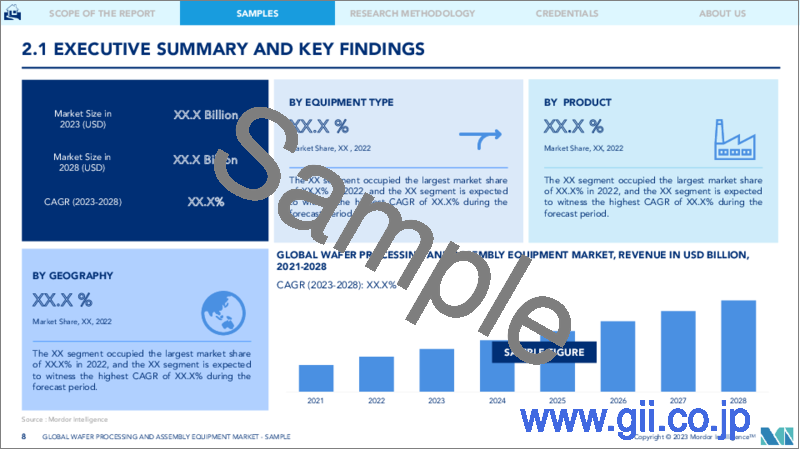
ウエハー処理・組立装置の世界市場は、2022年から2027年の予測期間中にCAGR8.4%で成長すると予測されています。
ウエハー処理・組立装置市場は、民生用電子機器の需要増に対応した成長が見込まれます。電子製品の需要増に伴い、新しい電子ガジェットの品質向上に対する顧客の期待が高まっています。識別タグやスマートカードなど、いくつかの民生用電子機器やIDソリューションでは、RFIDと集積回路製造用ウエハーを組み合わせています。電子製品へのシームレスな統合のため、超平滑表面と小型ウエハーの需要が高まっています。
主なハイライト
- Indian Brand Equity Foundationによると、2022年のインドの家電・民生機器(ACE)部門は、CAGR(CAGR)9%で3兆1500億インドルピー(483億7,000万米ドル)に成長すると予測されています。また、インドの電子機器製造業は、2024-25年には3,000億米ドル(22.5lakh crore)に達すると予測されています。さらに、民生用電子機器の使用と消費の増加が半導体需要を刺激し、予測期間を通じてウエハー処理・組立装置市場の収益を押し上げると予測されます。
- ウエハー処理・組立装置業界の顕著な動向は、より高いデバイス性能を持つ小型化されたウエハーに対する需要の高まりです。例えば、ウェーハは最終的に数十マイクロメートルの厚さにまで平坦化されます。メモリーやCIS、パワー系に使用される半導体ウエハーの多くは、100μmから200μmの厚さにまで薄型化されています。メモリーデバイスの場合、単一パッケージのメモリー容量を最大化する必要性、データ転送速度の向上、モバイルアプリケーションを中心とした電力消費などにより、さらなる薄型化が求められています。2次元NAND/DRAMなどの標準的なメモリーデバイスには、200μmを超える厚さのシリコンウエハが使用されています。
- 各地域の政府機関が半導体生産への投資を計画しており、研究対象市場の成長機会を生み出す可能性があります。例えば、2021年9月、ドイツ経済省は、EUの「欧州共通利益の重要プロジェクト」構想(投資を活性化し輸入依存度を下げるためのEUの主要補助金手段の一つ)に30億ユーロを投資する意思があることを表明しました。この資金は、ドイツ政府が新しい半導体製造工場を建設するために使用される予定です。この投資は、将来の半導体需要のうち、輸入半導体への依存を減らすことを主な目的としています。このような政府の政策が、研究対象市場を大きく動かすことになるでしょう。
- ウェハーには、製材、手作業、液体噴射、搬送システム、ピック・アンド・プレース装置など、ウェハーの製造サイクルにおいて機械的な負荷がかかります。現在市販されているパワー半導体は、一般的に厚さ50~100μmの200mmウェハーで製造されていますが、ロードマップでは1μmまでの薄型ウェハーも可能です。このウェーハの裏面を機械的に研磨します。研磨痕、研磨不良によるエッジチップ、スタークラック、砥石に巻き込まれたエッジパーティクルによるコメット、パーティクルの埋め込み、クレバージュラインなど、研磨工程で発生するさまざまな欠陥があります。
- さらに、COVID-19の大流行により世界的にウエハー半導体が不足していることから、各社は生産能力の増強に力を注いでいます。例えば、SMIC(Semiconductor Manufacturing International Corp)は、2021年9月に上海の自由貿易区に新工場を設立することを発表するなど、各都市にチップ製造工場を建設し、2025年までに生産能力を倍増させる積極的な計画を立てています。
ウエハー処理・組立装置の市場動向
薄膜蒸着が市場を牽引する要因の一つ
- 半導体や薄膜の製造には、CVD(Chemical Vapor Deposition)技術が一般的に採用されています。CVD装置市場の拡大には、マイクロエレクトロニクスベースの消費財の需要増加による半導体、LED、ストレージデバイス産業の急成長と、電気めっき用のCr6の厳しい使用制限が主に寄与しています。
- 2022年1月、韓国の特殊真空炉メーカーであるサームバック社は、900℃から2400℃までの温度で使用できるCVD装置のプロセス技術や設計・製造技術を開発し、国内外の顧客のニーズに応え続けています。これは、半導体、太陽光発電、携帯電話、航空宇宙、防衛などのハイテク産業において、高温耐熱のCVD部材の需要が高まっていることに対応するものです。
- リニアスパッタリング装置は、太陽エネルギー、ディスプレイ、データストレージ、半導体などの用途で使用されています。例えば、2021年12月、ボッシュは、世界中の自動車メーカーに供給するSic系パワー半導体の量産を開始しました。このような半導体の需要増加に対応するため、2021年にはロイトリンゲンのボッシュ・ウェハー工場のクリーンルーム・スペースに10,764平方フィートがすでに追加されています。2023年末までにはさらに32,292平方フィートが追加される予定です。このような半導体の増産は、調査済み市場を牽引します。
- 地域の自動車産業の進歩は、市場成長のための大きな機会を生み出すと予想されます。例えば、ドバイは最近、2030年までにエミレーツの街角に4万2000台のEVを走らせるというキャンペーンを開始しました。スパッタリング装置は、駆動系ベアリングやコンポーネントのコーティングに使用されており、EV車の開発が増加するにつれて、調査された市場を大幅に後押しすることになります。
- スパッタリング薄膜は、バイオメディカル用途にますます使用されるようになってきています。例えば、円筒形マグネトロンスパッタリングは、医療用ステントのバッチに保護膜を成膜するために使用されています。ナノ薄膜は、エレクトロニクス、繊維、医薬品、セラミックス、その他様々な用途に広く採用されています。ナノフィルムでコーティングされた布地は、化学気相成長法、ゾル-ゲル法、マグネトロンスパッタリング法で作られることが多いです。例えば、マグネトロンスパッタリング法は、膜厚制御、高純度、高速・低温、優れた接着性、操作性、環境への配慮などの利点を備えています。
アジア太平洋地域が市場の主要シェアを占める
- アジア太平洋地域は、世界で最も急成長している半導体市場です。中国、韓国、シンガポールなどからのスマートフォンや家電製品の強い需要に応えるため、多くのベンダーが同地域に生産施設を設置しています。
- 各社は、顧客の幅広いニーズに応えるため、新たなプロジェクトを開始し、同地域でのプレゼンスを拡大しています。例えば、2021年9月、UTAC Holding, Ltd.は、最先端のプラズマダイシングとマルチプロジェクトウェハー(MPW)機能を、一連の高度な半導体製造ソリューションに追加しました。プラズマダイシングは、チップ間のスクライブライン幅を狭め、ウエハー当たりのチップ数を増加させます。また、欠けや割れのない「ほぼ完璧な」切断品質が得られるため、慢性的な側壁品質の問題を抱える従来のメカニカルソーイングプロセスと比較して、明らかな優位性を持っています。
- さらに公的機関や非公開会社は、新製品や研究開発施設に投資しています。例えば、2021年9月、中国最大の受託チップメーカーであるSemiconductor Manufacturing International Corp(SMIC)は、上海の自由貿易区の一部である林港特別区と同社が合意したことを発表しています。この合意により、SMICは月産10万枚の12インチウエハーを生産する新ファウンドリーを設立する予定です。また、2021年3月には、深圳市政府と連携して、28nm(ナノメートル)以上の集積回路を生産する月産4万枚の12インチウエハーの製造施設に23億5000万米ドルを投資すると発表しています。
- 同様に、2021年10月、ニューサウスウェールズ州政府は、世界の半導体産業はオーストラリアの主要企業が不足していると認識し、この分野の重要な雇用の実現性を高めるために新しいセンターを計画します。この拠点「半導体セクターサービス局(S3B)」は、シドニーのテックセントラルに拠点を置き、州政府が資金を提供する予定です。さらに、主任研究員兼技術者室は、国内の半導体シーンを調査した結果、現在、半導体設計や半導体開発を中核事業とするオーストラリアの大手企業が存在しないことに言及しました。新拠点は、同国のウエハー加工・ダイシング装置市場を活用したものです。
- 携帯電話や無線・ネットワーク機器など、低消費電力で高性能な機器にTSV(Through Silicon Via)技術が普及するにつれ、ステルスダイシング装置の需要が高まっています。TSVは、上記アプリケーションのように2.5次元/3次元のパッケージングが可能なため、TSV Assembly/Packaging(ステルスダイシング等を用いたチップ間/チップ・ウェーハ間組立)に有効な装置です。メモリーやロジックでは、レーザーダイシングとブレードダイシングの組み合わせで使用されます。
ウエハー処理・組立装置市場の競合分析
世界のウエハー処理・組立装置市場は、適度に集約されています。プレーヤーは、異なる業界の変化する需要に対応するため、製品提供の革新に投資する傾向があります。さらに、プレーヤーは、その存在を拡大するために、パートナーシップ、合併、買収などの戦略的活動を採用しています。市場の最近の開拓は以下の通りです。
- 2022年3月-SK siltronは、米国ミシガン州ベイシティにある炭化ケイ素(SiC)半導体ウエハー製造工場の稼働開始を発表しました。年間6万枚程度の生産を計画しています。また、6インチSiCウエハーが主力製品。
- 2021年9月-Infineon Technologies AGは、オーストリアのFillachサイトに300ミリの薄型ウエハーでパワー半導体デバイスを製造するハイテクチップ工場を立ち上げました。16億ユーロの投資額は、欧州のマイクロエレクトロニクス分野で最大級のプロジェクトとなります。同社によると、同工場の産業用半導体の年間生産能力は、ドイツの年間電力消費量の約3倍に相当する約1,500TWhの電力を生産する太陽光発電システムの設備に十分対応できると言われています。
その他の特典
- エクセル形式の市場予測(ME)シート
- アナリストによる3ヶ月間のサポート
目次
第1章 イントロダクション
- 調査の前提および市場の定義
- 調査対象範囲
第2章 調査手法
第3章 エグゼクティブサマリー
第4章 マーケットインサイト
- 市場概要
- 産業の魅力- ポーターのファイブフォース分析
- 供給企業の交渉力
- 買い手の交渉力
- 新規参入業者の脅威
- 代替品の脅威
- 競争企業間の敵対関係
- COVID-19が市場に与える影響の評価
第5章 市場力学
- 市場促進要因
- 消費者のニーズの高まり
電子デバイスのニーズの高まりが
製造の展望を後押し
- 人工知能の普及
人工知能、IoT、コネクテッドデバイスの
業界別デバイスの急増
- 市場の課題
- テクノロジーのダイナミックな性質
製造装置の数回の変更が必要
製造装置
第6章 市場セグメンテーション
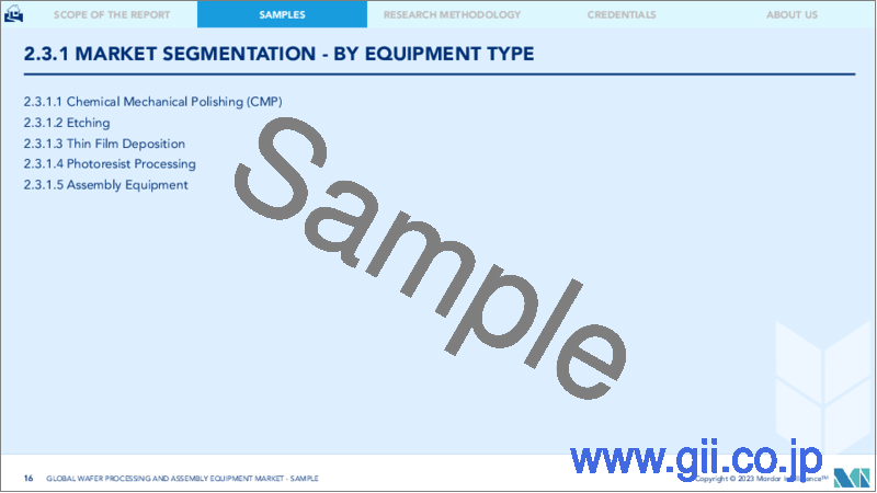
- 装置タイプ別
- 化学機械研磨
(CMP)
- エッチング
- 薄膜形成
- CVD
- スパッタリング
- その他
- フォトレジスト加工
- 組立装置
- ダイ・アタッチ
- ワイヤーボンディング
- パッケージング
- 検査・ダイシング
メッキなど
- 地域別情報
- アジア太平洋地域
- 北米
- 世界のその他の地域
- 製品別- ウエハー処理装置
- DRAM
- NAND
- ファウンドリ/ロジック
- その他の製品
第7章 ベンダーランキング分析
第8章 競争情勢
- 企業プロファイル
- Applied Materials Inc
- ASML Holding Semiconductor Company
- Tokyo Electron Limited
- Lam Research Corporation
- KLA Corporation
- Hitachi High-Technologies Corporation
- Disco Corporation
- ASM Pacific Technology
- Kulicke and Soffa Industries, Inc
- BE Semiconductor Industries N.V
- Towa Corporation
第9章 投資分析
第10章 投資分析市場の将来性
The Global Wafer Processing and Assembly Equipment Market is expected to grow at a CAGR of 8.4% during the forecast period of 2022 to 2027. The wafer processing and assembly equipment market is expected to grow in response to rising consumer electronics demand. Customer expectations for improved qualities of new electronic gadgets have risen as demand for electronic products has increased. Several consumer electronics and identity solutions, such as identification tags, smart cards, and others, combine RFIDs with wafers for integrated circuit fabrication. Customers increasingly demand ultra-smooth surfaces and smaller wafers for seamless integration into electronic products.
Key Highlights
- According to the Indian Brand Equity Foundation, In 2022, the Indian appliance and consumer electronics (ACE) sector is predicted to grow at a 9% compound annual growth rate (CAGR) to INR 3.15 trillion (USD 48.37 billion). The Indian electronics manufacturing sector is expected to reach USD 300 billion (INR 22.5 lakh crore) by 2024-25. Furthermore, increased consumer electronics device usage and consumption are predicted to fuel semiconductor demand, boosting wafer processing and assembly equipment market revenues throughout the projection period.
- A prominent trend in the wafer processing and assembly equipment industry is the growing demand for miniaturized wafers with higher device performance. Wafers, for example, are flattened down to final thicknesses of tens of micrometers. Most semiconductor wafers used in memory, CIS, and power applications are reduced to 100 µm-200 µm in thickness. In the case of memory devices, further thickness reduction is required due to the need to maximize the memory capacity of single packages, increased data transmission rates, and power consumption fueled mostly by mobile applications. Silicon wafers thicker than 200 µm are used in standard memory devices like 2D NAND/DRAM.
- The government bodies in the different regions are planning to invest in the production of semiconductors, which may create an opportunity for the studied market to grow. For instance, in September 2021, Germany's economy ministry stated that the country is willing to invest EUR 3 billion in the EU's "Important Projects of Common European Interest" initiative, which is one of the EU's primary subsidy tools for stimulating investment and reducing import dependency. The money will be used by the German government to build new semiconductor manufacturing factories. This investment is primarily aimed at reducing dependency on imported semiconductors for future semiconductor needs. Government policies like this will significantly drive the studied market.
- Wafers are subjected to mechanical loads induced by sawing, manual handling, liquid jets, transport systems, and pick and place equipment during the wafer manufacturing cycle. Power semiconductors on the market now are generally made on 200-mm wafers with thicknesses ranging from 50 to 100 µm, although their roadmaps allow for wafers as thin as 1 µm. Mechanical polishing thins the backside of these wafers. Grinding marks, grinding failures resulting in edge chips, star cracks, and comets generated by edge particles caught in the grinding wheel, embedded particles, cleavage lines, and a variety of other faults are all defects caused by the polishing process.
- Furthermore, the global shortage of wafer semiconductors led by the COVID-19 pandemic has encouraged players to focus on increasing production capacity. For instance, Semiconductor Manufacturing International Corp (SMIC) has indulged in aggressive plans to double its production capacity by 2025 by constructing new chip fabrication plants in different cities, including its announcement in September 2021 to establish a new factory in Shanghai's free trade zone.
Wafer Processing & Assembly Equipment Market Trends
Thin Film Deposition is One of the Factor Driving the Market
- The Chemical Vapor Deposition (CVD) technology is commonly employed in the fabrication of semiconductors and thin films. The expansion of the CVD equipment market is primarily driven by increasing demand for microelectronics-based consumer items, which is resulting in quicker growth of the semiconductor, LED, and storage device industries, as well as severe limits on the use of Cr6 for electroplating.
- In January 2022, ThermVac Inc., a Korean manufacturer of special vacuum furnaces, continues to respond to the needs of domestic and international clients by developing process technology and design and manufacturing technology for CVD equipment that can be used at temperatures ranging from 900°C to 2,400°C. This corresponds to the growing demand for high-temperature heat-resistant CVD components in high-tech industries like semiconductors, solar power, mobile phones, aerospace, and defense.
- The linear sputtering equipment is used in applications like solar energy, display, Data storage, semiconductor, and many more. For instance, in December 2021, Bosch started the volume production of Sic-based power semiconductors supplying automotive manufacturers worldwide. To meet the increasing demand for such semiconductors, an extra 10,764 square feet were already added to the clean-room space at the Bosch wafer fab in Reutlingen in 2021. Another 32,292 square feet will be added by the end of 2023. Such an increase in the production of semiconductors will drive the studied market.
- The advancements in the regional automotive industry are expected to create significant opportunities for market growth. For instance, Dubai recently launched a campaign to have 42,000 EVs on the streets of Emirates by 2030. The sputtering equipment is used in the coating of Drive train bearings and components as the increase in the developments of EV vehicles will significantly drive the studied market.
- Sputtered thin films are increasingly being used in biomedical applications. An example is a cylindrical magnetron sputtering to deposit protective coatings on batches of medical stents. Nano-films are widely employed in electronics, textiles, pharmaceuticals, ceramics, and various other applications. Fabrics coated with Nanofilm are often created by chemical vapor deposition, sol-gel technique, and magnetron sputtering. The magnetron sputtering method, for example, offers the benefits of controlled film thickness, high purity, high speed and low temperature, excellent adhesion, ease of operation, and environmental friendliness, among others.
Asia Pacific Holds the Major Share of the Market
- Asia-Pacific has the world's fastest-growing semiconductor market. Many vendors are setting up production facilities in the region in response to strong demand for smartphones and other consumer electronics gadgets from nations including China, the Republic of Korea, and Singapore.
- The companies are expanding their presence in the region by starting new projects to cater to the wide need of the customer. For instance, in September 2021, UTAC Holding, Ltd. added state-of-the-art plasma dicing and multi-project wafer (MPW) capabilities to a range of advanced semiconductor manufacturing solutions. Plasma dicing narrows the scribe line width between chips and increases the number of chips per wafer. Also, it provides "nearly perfect" cutting quality with no chips or cracks, which is a clear advantage over traditional mechanical sawing processes that lead to chronic sidewall quality issues.
- Further public agencies and private companies are investing in new products and research & development facilities. For instance, In September 2021, China's largest contract chipmaker Semiconductor Manufacturing International Corp (SMIC) announced the company's agreement with the Lin-Gang Special area-part of Shanghai's free trade zone. This agreement enables SMIC to establish a new foundry with a monthly planned capacity of 100,000 12-inch wafers. Also, in March 2021, the company announced an investment of USD 2.35 billion in coordination with the Shenzhen government for a manufacturing facility to produce 28nanometre (nm) and above integrated circuits with a monthly capacity of 40,000 12-inch wafers.
- Similarly, in October 2021, the Government of New South Wales is aware that the global semiconductor industry lacks Australia's major players and plans a new center to improve the feasibility of critical jobs in this sector. The hub, the Semiconductor Sector Service Bureau (S3B), will be based in Sydney's Tech Central and be funded by the state government. Further, Chief Scientist and Engineer Office, after researching the national semiconductor scene, mentioned there are currently no major Australian companies with semiconductor design or semiconductor development as their core business. The new hub leverages the country's wafer processing and dicing equipment market.
- The demand for stealth dicing equipment is growing as TSV (Through Silicon Via) technology becomes more prevalent for low-power, high-performance devices such as mobile phones and other wireless and networking devices. As TSV can package 2.5/3D for the applications listed above, the equipment is useful for TSV Assembly/Packaging (chip-to-chip and chip-to-wafer assembly with stealth dicing and other processes). In Memory and Logic, a combination of laser dicing and blade dicing is used.
Wafer Processing & Assembly Equipment Market Competitor Analysis
The Global Wafer Processing and Assembly Equipment market is moderately consolidated. Players tend to invest in innovating their product offerings to cater to the different industry's changing demands. Moreover, players adopt strategic activities like partnerships, mergers, and acquisitions to expand their presence. Some of the recent developments in the market are:
- March 2022 - SK siltron announced the beginning of the operation of the Silicon carbide (SiC) semiconductor wafer manufacturing plant in Bay City, Michigan, US. The company has a plan to produce around 60,000 annually. Also, a 6-inch SiC wafer is the main product of the company.
- September 2021 - Infineon Technologies AG launched its high-tech chip factory for power semiconductor devices on 300-millimeter thin wafers at its Villach site in Austria. At EUR 1.6 billion, the investment made by the company represents one of the largest such projects in the microelectronics sector in Europe. According to the company, the annual capacity planned for industrial semiconductors from the facility is sufficient to equip solar systems producing a total of around 1,500 TWh of electricity, which is around three times the annual power consumption of Germany.
Additional Benefits:
- The market estimate (ME) sheet in Excel format
- 3 months of analyst support
TABLE OF CONTENTS
1 INTRODUCTION
- 1.1 Study Assumption And Market Defination
- 1.2 Scope of the study
2 RESEARCH METHODOLOGY
3 EXECUTIVE SUMMARY
4 MARKET INSIGHTS
- 4.1 Market Overview
- 4.2 Industry Attractiveness - Porter's Five Forces Analysis
- 4.2.1 Bargaining Power Of Suppliers
- 4.2.2 Bargaining Power Of Buyers
- 4.2.3 Threat Of New Entrants
- 4.2.4 Threat Of Substitutes
- 4.2.5 Intensity Of Competitive Rivalry
- 4.3 Assessment of the Impact of Covid-19 on the Market
5 MARKET DYNAMICS
- 5.1 Market Drivers
- 5.1.1 Increasing Needs of Consumer
Electronic Devices Boosting the
Manufacturing Prospects
- 5.1.2 Proliferation of Artificial
Intelligence, IoT and Connected
Devices across Industry Verticals
- 5.2 Market Challenges
- 5.2.1 Dynamic Nature of Technologies
Requires Several Changes in
Manufacturing Equipment
6 MARKET SEGMENTATION
- 6.1 By Equipment Type
- 6.1.1 Chemical Mechanical Polishing
(CMP)
- 6.1.2 Etching
- 6.1.3 Thin Film Deposition
- 6.1.3.1 CVD
- 6.1.3.2 Sputter
- 6.1.3.3 Other Type
- 6.1.4 Photoresist Processing
- 6.1.5 Assembly Equipment
- 6.1.5.1 Die Attach
- 6.1.5.2 Wire Bonding
- 6.1.5.3 Packaging
- 6.1.5.4 Inspection, Dicing,
Plating and Others
- 6.2 By Geography
- 6.2.1 Asia-Pacific
- 6.2.2 North America
- 6.2.3 Rest of the World
- 6.3 By Product - Wafer Processing Equipment
- 6.3.1 DRAM
- 6.3.2 NAND
- 6.3.3 Foundry/Logic
- 6.3.4 Other Products
7 VENDOR RANKING ANALYSIS
8 COMPETITIVE LANDSCAPE
- 8.1 Company Profiles
- 8.1.1 Applied Materials Inc
- 8.1.2 ASML Holding Semiconductor Company
- 8.1.3 Tokyo Electron Limited
- 8.1.4 Lam Research Corporation
- 8.1.5 KLA Corporation
- 8.1.6 Hitachi High-Technologies Corporation
- 8.1.7 Disco Corporation
- 8.1.8 ASM Pacific Technology
- 8.1.9 Kulicke and Soffa Industries, Inc
- 8.1.10 BE Semiconductor Industries N.V
- 8.1.11 Towa Corporation