|
|
市場調査レポート
商品コード
1457078
半導体リードフレーム市場:2024年から2029年までの予測Semiconductor Lead Frame Market - Forecasts from 2024 to 2029 |
||||||
|
|
|||||||
カスタマイズ可能
|
|||||||


| 半導体リードフレーム市場:2024年から2029年までの予測 |
|
出版日: 2024年02月09日
発行: Knowledge Sourcing Intelligence
ページ情報: 英文 135 Pages
納期: 即日から翌営業日
|

- 全表示
- 概要
- 目次
半導体リードフレーム市場はCAGR 4.99%で成長し、2022年の31億7,400万米ドルから2029年には44億6,200万米ドルに達すると予測されています。
半導体リードフレームは、半導体デバイスの集積回路(IC)、ディスクリートデバイス、その他のコンポーネントを支持し、接続する金属製の小型で平坦な構造体です。リードフレームは、ICと周辺環境の間を電気信号が通過する経路を記載しています。信頼性の高い接続性と効率的な性能を保証するため、半導体デバイスの製造には欠かせない部品です。半導体リードフレーム市場の成長の原動力は、電子機器に対する需要の増加と、電子機器の小型化・複雑化に伴う電子部品の小型化傾向の高まりです。
市場の促進要因
- 先進パッケージング技術の利用拡大が市場拡大の原動力となっています。
ワイヤーボンディングなどの先進パッケージング技術の利用が増加していることが、半導体リードフレーム市場の成長を促す大きな要因となっています。ワイヤーボンディング技術の精度向上により、半導体業界全体での需要拡大が見込まれています。例えば、2022年9月、Henniker Plasma Companyは、ワイヤーボンディング技術の効率を向上させるプラズマに基づく新しい処理を発表しました。さらに、自動車用照明やその他のディスプレイによるLED需要の高まりは、半導体リードフレームの需要を刺激しています。半導体リードフレームは、最適な電気的接続性と性能を確保するためにワイヤの正確な配置や配線に対応できるため、LEDパッケージングに使用されることが多いからです。例えば、2022年9月、ドイツを拠点とする照明ソリューション製造企業、オスラムリヒトAGは、自動車照明に使用されるオスロンブラックフラットS製品群に、リードフレームベースのLED照明部品を導入しました。このため、LED需要の増加を背景としたワイヤボンディングパッケージング技術に対する需要の高まりが、予測期間を通じて半導体リードフレーム市場を牽引すると見られています。
技術別では、スタンピングが突出した市場シェアを占めると予想されます。
スタンピング技術では、金属シートや箔を金型に押し付けて所望のパターンや形態を作成します。高速でコスト効率に優れたプロセスであり、大量のリードフレームを迅速かつ効率的に生産できるため、スマートフォンやタブレット端末などの民生用電子機器のリードフレーム生産に主に利用されています。スマートフォンやタブレット端末の需要の増加は、スタンピング技術の消費を増加させると予想されます。さらに、半導体リードフレーム市場におけるスタンピング技術セグメントは、高性能で小型化された電子機器の需要と、さまざまな電子製品の精密な要件に対応するための小型・軽量のリードフレームに対する高い需要によって牽引されています。
アジア太平洋が半導体リードフレーム市場で大きなシェアを占める
アジア太平洋の様々な国々における半導体産業の拡大が、半導体リードフレーム市場を牽引すると予想されています。半導体需要の増加に伴い、リードフレームとしてそのような半導体を製造するために使用される様々な機器の需要が増加しているためです。例えば、世界半導体貿易が発表したデータによると、台湾の半導体産業は2022年第3四半期に6,255億3,000万台湾ドルの売上高を達成しました。また、国際貿易局が発表したところによると、日本の半導体セクターは2020~2021年にかけて19.8%増となり、世界の半導体生産量の9%近くを占めました。さらに、インド政府の報道情報局が2022年に発表した声明によると、インドの半導体市場は2020年の150億米ドルから2026年には630億米ドルに増加するといいます。
市場の課題
- 半導体部品の代替供給と不足は、市場成長にとって依然として大きな課題です。
ファンアウト・ウエハーレベル・パッケージング(FOWLP)やシステムインパッケージ(SiP)ソリューションなどの代替パッケージング技術の利用が増加しているが、これらの技術は従来のリードフレームベースのパッケージングに比べて、集積度の向上や熱性能の改善などいくつかの利点があるため、半導体リードフレーム市場の成長を制限しています。例えば、サムスン電子は、2023年4月に日本の生産施設にファンアウト・ウエハーレベル・パッケージングを導入するために7,500万米ドルを投資すると発表しました。その結果、複数の半導体・エレクトロニクス企業がリードフレームベースのパッケージングソリューションからこれらの代替品に移行しつつあり、予測期間中の市場の減速が予想されます。
さらに、半導体部品の不足が続いており、半導体デバイスとその製造に使用される部品(リードフレームを含む)の需要全体に影響を及ぼしているため、半導体リードフレーム市場に影響を与えています。この不足は、特定のメーカーが製品を生産するために必要な材料や資源を確保するために、価格を上昇させ、生産難易度を高めています。
製品の提供
- 株式会社Toppan Inc.の半導体リードフレーム-印刷事業を手がけるToppan Inc.は、半導体パッケージ基板製品部門において、ファインピッチリードフレーム、ダウンセットリードフレーム、ヒートスプレッダ付きリードフレーム、樹脂接着改良パッケージ、カシメリードフレーム、QFN基板の6種類のリードフレーム製品を製造しており、半導体プロセスの多様なニーズに対応しています。
- Advanced Assembly Materials International Ltd.の半導体リードフレーム。-香港を拠点とし、さまざまな半導体パッケージング要件に対応する特殊製品を提供するAdvanced Assembly Materials International Ltd.は、顧客の仕様に合わせて最大100x300mmまでのさまざまなサイズの高密度でコスト効率の高いリードフレームを製造しています。
- SDI Group, Inc.の半導体リードフレームSDI Group Inc.は、さまざまな特殊科学製品を製造する台湾の企業で、IC、ディスクリート/トランジスタ、その他の半導体チップ用途向けに3種類のリードフレームを製造しています。同社が製造するディスクリートリードフレームは、自動車コンピュータの制御システムに広く採用されています。
目次
第1章 イントロダクション
- 市場概要
- 市場の定義
- 調査範囲
- 市場セグメンテーション
- 通貨
- 前提条件
- 基準年と予測年のタイムライン
- 関係者にとっての主要メリット
第2章 調査手法
- 調査デザイン
- 調査プロセス
第3章 エグゼクティブサマリー
- 主要調査結果
- アナリストビュー
第4章 市場力学
- 市場促進要因
- 市場抑制要因
- ポーターのファイブフォース分析
- 業界バリューチェーン分析
- アナリストビュー
第5章 半導体リードフレーム市場:技術別
- イントロダクション
- 化学エッチング
- スタンピング
第6章 半導体リードフレーム市場:用途別
- イントロダクション
- 集積回路
- ディスクリートデバイス
- その他
第7章 半導体リードフレーム市場:地域別
- イントロダクション
- 北米
- 南米
- 欧州
- 中東・アフリカ
- アジア太平洋
第8章 競合環境と分析
- 主要企業と戦略分析
- 市場シェア分析
- 合併、買収、合意とコラボレーション
- 競合ダッシュボード
第9章 企業プロファイル
- Toppan Inc.
- Advanced Assembly Materials International Ltd.
- SDI Group, Inc.
- SHINKO ELECTRIC INDUSTRIES CO., LTD.(Fujitsu)
- Mitsui High-tec, Inc.
- Precision Micro Ltd.
- Amkor Technology
- QPL Electronics Factory
- Ningbo Kangqiang Electronics Co., LTD.
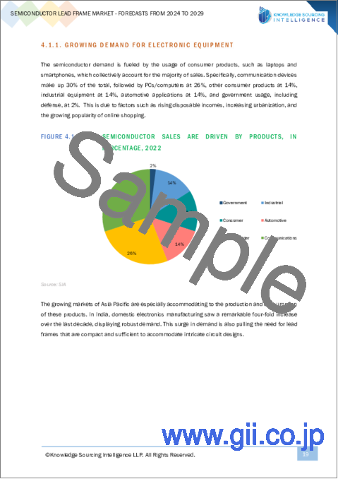
The semiconductor lead frame market is projected to grow at a CAGR of 4.99% to reach US$4.462 billion in 2029 from US$3.174 billion in 2022.
A semiconductor lead frame is a small, flat structure made of metal that supports and connects the integrated circuit (IC), discrete devices, and other components in semiconductor devices. The lead frame provides a pathway for electrical signals to pass between the IC and the peripheral environment. They are an essential component in the manufacturing of semiconductor devices as they ensure reliable connectivity and efficient performance. The growth of the semiconductor lead frame market is driven by the increasing demand for electronic devices and the growing trend towards miniaturization of electronic components since the reduction in the size and increasing complexity of electronic devices are creating a high demand for smaller and precise lead frames.
Market Drivers
- Increasing use of advanced packaging technologies is driving the market expansion.
The increasing use of advanced packaging technologies, such as wire bonding, is a significant factor driving the growth of the semiconductor lead frame market. Improving the accuracy of wire bonding technology is expected to increase its demand across the semiconductor industry. For instance, in September 2022, Henniker Plasma Company announced a new treatment based on plasma to improve the efficiency of wire bonding technology. In addition, the rising demand for LEDs driven by automotive lighting and other displays is stimulating the demand for semiconductor lead frames as semiconductor lead frames are often used in LED packaging due to their ability to accommodate the precise placement and routing of the wires to ensure the optimal electrical connectivity and performance. For instance, in September 2022, a German-based light solutions manufacturing company, OSRAM Licht AG, introduced lead-frame-based LED lighting components to its Oslon Black Flat S product range used for automotive lighting. Therefore, the rising demand for wire bonding packaging technologies driven by increasing demand for LEDs is expected to drive the semiconductor lead frame market over the forecast period.
By technology, the stamping is expected to hold a prominent market share.
Stamping technology involves pressing a metal sheet or foil against a die to create the desired pattern or shape. It is a fast and cost-effective process that can produce large volumes of lead frames quickly and efficiently and, therefore, is majorly utilized in producing lead frames for consumer electronics such as smartphones and tablets. The rising demand for smartphones and tablets is anticipated to increase the consumption of stamping technology. Further, the stamping technology sector in the semiconductor lead frame market is driven by the demand for high-performance and miniaturized electronic devices and the high demand for lead frames that are small and lightweight to accommodate the precise requirements of various electronic products.
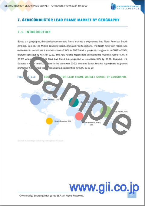
Asia Pacific region held a substantial share in the semiconductor lead frame market
The expansion of the semiconductor industry in different countries in the Asia Pacific region is expected to drive the semiconductor lead frame market as the increasing demand for semiconductors is followed by a rise in demand for various equipment used to manufacture such semiconductors as lead frames. For instance, the semiconductor industry in Taiwan achieved sales revenues of TWD625.53 billion in the third quarter of 2022, according to data released by the World Semiconductor Trade. In addition, the Japanese semiconductor sector, as reported by the International Trade Administration, witnessed a 19.8% rise between 2020 and 2021, accounting for nearly 9% of the total world semiconductor production. Further, according to a statement released by the Press Information Bureau of the Indian government in 2022, India's semiconductor market will increase from US$15 billion in 2020 to US$63 billion by 2026.
Market Challenge
- Alternative availability and the scarcity of semiconductor components remains significant challenge to the market growth.
The increasing use of alternative packaging technologies, such as fan-out wafer-level packaging (FOWLP) and system-in-package (SiP) solutions, is limiting the semiconductor lead frame market growth since these technologies offer several advantages over traditional lead frame-based packaging, such as higher levels of integration and improved thermal performance. For instance, Samsung Electronics announced an investment of US$75 million to deploy fan-out wafer-level packaging at its production facility in Japan in April 2023. Consequently, several semiconductor and electronics companies are shifting from lead frame-based packaging solutions to these alternatives is expected to slow down the market over the forecast period.
In addition, the ongoing shortage of semiconductor components is impacting the semiconductor lead frame market as it is affecting the overall demand for semiconductor devices and the components used to manufacture them, including lead frames. The shortage is rising the prices and increasing production difficulty for certain manufacturers to secure the necessary materials and resources to produce their products.
Product Offerings:
- Semiconductor lead frame by Toppan Inc. - Toppan Inc., a Japan-based company involved in the printing business, manufactures six different lead frame products, namely Fine Pitch Leadframe, Downset Leadframe, Leadframe with Heat Spreader, Resin Adhesion Improved Package, Caulking Leadframe, and QFN Substrate under its semiconductor package substrates product division to meet the varying needs of different semiconductor processes.
- Semiconductor lead frame by Advanced Assembly Materials International Ltd. - Advanced Assembly Materials International Ltd., a Hong-Kong-based company offering specialty products to various semiconductor packaging requirements, manufactures lead frames of high-density and cost-effective nature of varying sizes up to 100x300mm as per the specifications of its customers.
- Semiconductor lead frame by SDI Group, Inc. - SDI Group Inc., a Taiwanese company generating various specialty scientific products, manufactures three different lead frame types for ICs, discrete/transistors, and other semiconductor chip applications. The discrete lead frames manufactured by the company are extensively adopted in control systems of auto-computers.
Segmentation:
By Technology
- Chemical Etching
- Stamping
By Application
- Integrated Circuit (IC)
- Discrete Devices
- Others
By Geography
- North America
- USA
- Canada
- Mexico
- South America
- Brazil
- Argentina
- Others
- Europe
- Germany
- France
- United Kingdom
- Spain
- Others
- Middle East and Africa
- Saudi Arabia
- UAE
- Israel
- Others
- Asia Pacific
- China
- Japan
- India
- South Korea
- Taiwan
- Others
TABLE OF CONTENTS
1. INTRODUCTION
- 1.1. Market Overview
- 1.2. Market Definition
- 1.3. Scope of the Study
- 1.4. Market Segmentation
- 1.5. Currency
- 1.6. Assumptions
- 1.7. Base, and Forecast Years Timeline
- 1.8. Key Benefits for the stakeholder
2. RESEARCH METHODOLOGY
- 2.1. Research Design
- 2.2. Research Processes
3. EXECUTIVE SUMMARY
- 3.1. Key Findings
- 3.2. Analyst View
4. MARKET DYNAMICS
- 4.1. Market Drivers
- 4.2. Market Restraints
- 4.3. Porter's Five Forces Analysis
- 4.3.1. Bargaining Power of Suppliers
- 4.3.2. Bargaining Power of Buyers
- 4.3.3. Threat of New Entrants
- 4.3.4. Threat of Substitutes
- 4.3.5. Competitive Rivalry in the Industry
- 4.4. Industry Value Chain Analysis
- 4.5. Analyst View
5. SEMICONDUCTOR LEAD FRAME MARKET BY TECHNOLOGY
- 5.1. Introduction
- 5.2. Chemical Etching
- 5.2.1. Market Trends and Opportunities
- 5.2.2. Growth Prospects
- 5.2.3. Geographic Lucrativeness Insights
- 5.3. Stamping
- 5.3.1. Market Trends and Opportunities
- 5.3.2. Growth Prospects
- 5.3.3. Geographic Lucrativeness Insights
6. SEMICONDUCTOR LEAD FRAME MARKET BY APPLICATION
- 6.1. Introduction
- 6.2. Integrated Circuits
- 6.2.1. Market Trends and Opportunities
- 6.2.2. Growth Prospects
- 6.2.3. Geographic Lucrativeness Insights
- 6.3. Discrete Devices
- 6.3.1. Market Trends and Opportunities
- 6.3.2. Growth Prospects
- 6.3.3. Geographic Lucrativeness Insights
- 6.4. Others
- 6.4.1. Market Trends and Opportunities
- 6.4.2. Growth Prospects
- 6.4.3. Geographic Lucrativeness Insights
7. SEMICONDUCTOR LEAD FRAME MARKET BY GEOGRAPHY
- 7.1. Introduction
- 7.2. North America
- 7.2.1. By Technology
- 7.2.2. By Application
- 7.2.3. By Country
- 7.2.3.1. USA
- 7.2.3.1.1. Market Trends and Opportunities
- 7.2.3.1.2. Growth Prospects
- 7.2.3.2. Canada
- 7.2.3.2.1. Market Trends and Opportunities
- 7.2.3.2.2. Growth Prospects
- 7.2.3.3. Mexico
- 7.2.3.3.1. Market Trends and Opportunities
- 7.2.3.3.2. Growth Prospects
- 7.2.3.1. USA
- 7.3. South America
- 7.3.1. By Technology
- 7.3.2. By Application
- 7.3.3. By Country
- 7.3.3.1. Brazil
- 7.3.3.1.1. Market Trends and Opportunities
- 7.3.3.1.2. Growth Prospects
- 7.3.3.2. Argentina
- 7.3.3.2.1. Market Trends and Opportunities
- 7.3.3.2.2. Growth Prospects
- 7.3.3.3. Others
- 7.3.3.3.1. Market Trends and Opportunities
- 7.3.3.3.2. Growth Prospects
- 7.3.3.1. Brazil
- 7.4. Europe
- 7.4.1. By Technology
- 7.4.2. By Application
- 7.4.3. By Country
- 7.4.3.1. Germany
- 7.4.3.1.1. Market Trends and Opportunities
- 7.4.3.1.2. Growth Prospects
- 7.4.3.2. France
- 7.4.3.2.1. Market Trends and Opportunities
- 7.4.3.2.2. Growth Prospects
- 7.4.3.3. United KIngdom
- 7.4.3.3.1. Market Trends and Opportunities
- 7.4.3.3.2. Growth Prospects
- 7.4.3.4. Spain
- 7.4.3.4.1. Market Trends and Opportunities
- 7.4.3.4.2. Growth Prospects
- 7.4.3.5. Others
- 7.4.3.5.1. Market Trends and Opportunities
- 7.4.3.5.2. Growth Prospects
- 7.4.3.1. Germany
- 7.5. Middle East and Africa
- 7.5.1. By Technology
- 7.5.2. By Application
- 7.5.3. By Country
- 7.5.3.1. Saudi Arabia
- 7.5.3.1.1. Market Trends and Opportunities
- 7.5.3.1.2. Growth Prospects
- 7.5.3.2. UAE
- 7.5.3.2.1. Market Trends and Opportunities
- 7.5.3.2.2. Growth Prospects
- 7.5.3.3. Israel
- 7.5.3.3.1. Market Trends and Opportunities
- 7.5.3.3.2. Growth Prospects
- 7.5.3.4. Others
- 7.5.3.4.1. Market Trends and Opportunities
- 7.5.3.4.2. Growth Prospects
- 7.5.3.1. Saudi Arabia
- 7.6. Asia Pacific
- 7.6.1. By Technology
- 7.6.2. By Application
- 7.6.3. By Country
- 7.6.3.1. China
- 7.6.3.1.1. Market Trends and Opportunities
- 7.6.3.1.2. Growth Prospects
- 7.6.3.2. Japan
- 7.6.3.2.1. Market Trends and Opportunities
- 7.6.3.2.2. Growth Prospects
- 7.6.3.3. India
- 7.6.3.3.1. Market Trends and Opportunities
- 7.6.3.3.2. Growth Prospects
- 7.6.3.4. South Korea
- 7.6.3.4.1. Market Trends and Opportunities
- 7.6.3.4.2. Growth Prospects
- 7.6.3.5. Taiwan
- 7.6.3.5.1. Market Trends and Opportunities
- 7.6.3.5.2. Growth Prospects
- 7.6.3.6. Others
- 7.6.3.6.1. Market Trends and Opportunities
- 7.6.3.6.2. Growth Prospects
- 7.6.3.1. China
8. COMPETITIVE ENVIRONMENT AND ANALYSIS
- 8.1. Major Players and Strategy Analysis
- 8.2. Market Share Analysis
- 8.3. Mergers, Acquisitions, Agreements, and Collaborations
- 8.4. Competitive Dashboard
9. COMPANY PROFILES
- 9.1. Toppan Inc.
- 9.2. Advanced Assembly Materials International Ltd.
- 9.3. SDI Group, Inc.
- 9.4. SHINKO ELECTRIC INDUSTRIES CO., LTD. (Fujitsu)
- 9.5. Mitsui High-tec, Inc.
- 9.6. Precision Micro Ltd.
- 9.7. Amkor Technology
- 9.8. QPL Electronics Factory
- 9.9. Ningbo Kangqiang Electronics Co., LTD.