|
|
市場調査レポート
商品コード
1163371
半導体計測および検査装置の世界市場-市場規模、セグメント、展望、収益予測:タイプ別、組織規模別、地域別(2022年~2028年)Global Semiconductor Metrology and Inspection Equipment Market Size, Segments, Outlook, and Revenue Forecast 2022-2028 by Type, Organization Size, and Regions |
||||||
|
|
|||||||

| 半導体計測および検査装置の世界市場-市場規模、セグメント、展望、収益予測:タイプ別、組織規模別、地域別(2022年~2028年) |
|
出版日: 2022年11月29日
発行: Ken Research Private Limited
ページ情報: 英文
納期: お問合せ
|
- 全表示
- 概要
- 目次
世界の半導体計測および検査装置の市場規模は、予測期間(2022年~2028年)に7%のCAGRで成長し、2028年には150億米ドルに達すると予測されています。民生用電子機器における電子回路の小型化需要の高まり、スマートデバイスの用途拡大、産業オートメーションの台頭、自動車へのチップ搭載の普及は、市場の成長を促進しています。
当レポートでは、世界の半導体計測および検査装置市場について調査分析し、主要な動向、競合情勢、市場分析など、体系的な情報を提供しています。
目次
第1章 エグゼクティブサマリー
- 世界の半導体計測および検査装置市場のハイライト成長実績と予測
- 市場動向、課題、競合のハイライト
- 市場収益シェアのハイライト:セグメント別
第2章 市場概要と成長に影響を与える主要な動向
- 世界の半導体計測および検査装置市場の分類
- 業界のバリューチェーン
- 世界の半導体計測および検査装置市場における主要企業のエコシステム
- 政府の規制と開発
- 市場に影響を与える主要な促進要因と課題
- COVID-19が世界の半導体計測および検査装置市場に与える影響
- 全世界の半導体計測および検査装置市場の成長実績(2017年~2021年):セグメントタイプ別
- タイプ別
- 組織規模別
- 地域別
- 世界の半導体計測および検査装置市場の成長実績と予測(2017年~2028年)
- 重要ポイント
第3章 世界の市場セグメンテーション、成長実績、展望、予測:タイプ別
- 市場の定義-セグメンテーション:タイプ別
- 市場収益シェア、成長実績、展望、予測(2017年~2028年):タイプ別
- リソグラフィ計測
- ウエハー検査
- 薄膜計測
- その他のプロセス制御システム
- 市場セグメンテーションからの重要ポイント:タイプ別
第4章 世界の市場セグメンテーション、成長実績、展望、予測:組織規模別
- 市場の定義-セグメンテーション:組織規模別
- 市場収益シェア、成長実績、展望、予測(2017年~2028年):組織規模別
- 大企業<
- 小規模企業
- 市場セグメンテーションからの重要なポイント:組織規模別
第5章 業界/競合分析-競合情勢
- 企業(競合)の製品と競合のシェア
- 世界の半導体計測および検査機器の競合のポーターのファイブフォース分析
- 市場の成長に影響を与える世界の半導体計測および検査装置セクターの主な開発
- 世界の半導体計測および検査装置市場における主要な競合の比較(2021年)
- 世界の半導体計測および検査装置市場における主要な競合の比較(2021年):タイプ範囲別
- 世界の半導体計測および検査装置市場における主要な競合の比較(2021年):組織規模範囲別
- 世界の半導体計測および検査装置市場における主要な競合の比較(2021年):地域別
- 競合情勢からの重要ポイント
第6章 主要な競合企業プロファイル(会社概要、製品提供、SWOT分析)
- KLA Corporation
- Applied Materials Inc.
- Onto Innovation Inc.
- Thermo Fisher Scientific Inc.
- Hitachi High-Tech Corporation
- Nova Ltd.
- ASML Holding NV
- Lasertec Corporation
- JEOL Ltd.
- Nikon Metrology NV
- Camtek Limited
- Unity Semiconductor SAS
第7章 地域分析と主要地域市場の成長実績、展望、予測
- マクロ経済要因の主要地域比較
- 全世界市場収益シェア、成長実績、地域予測(2017年~2028年):地域別
- 主要地域の市場分析、成長実績、展望と予測(2017年~2028年)
- 北米-半導体計測および検査装置市場分析
- 欧州-半導体計測および検査装置市場分析
- アジア太平洋-半導体計測および検査装置市場分析
- ラテンアメリカ、中東、アフリカ-半導体計測および検査装置の市場分析
第8章 業界専門家の意見/展望
- 市場の現状と将来の展望に関する業界専門家と経営幹部の注目すべき声明/引用
第9章 アナリストの推奨
- 特定された主要な機会と機会から得られる可能性のある戦略に関するアナリストの推奨事項
第10章 付録
- 調査手法-市場規模の推定、予測、および健全性チェックのアプローチ
- サンプルディスカッションガイド
免責事項
Market Overview:
Semiconductor metrology instruments are designed for wafer and thin film in-line inspection after semiconductor processing. Semiconductor metrology instruments include ion manufactories, C- V systems, interferometers, source measure units (SME) magnetometers, optic and imaging systems, profilometers, reflectometers, resistance probes, and resistance high-energy electron diffraction (RHEED) systems, and X-ray diffractometers, among others.
According to Ken Research Analysis, the Global Semiconductor Metrology and Inspection Equipment Market is expected to record a positive CAGR of ~7% during the forecast period (2022-2028) and is expected to reach approximately US$ 15 billion by 2028.
The global semiconductor metrology and inspection equipment market is driven by the rising demand for the miniaturization of electronic circuits in consumer electronic devices is driving the demand for the studied market. Additionally growing smart devices application, rising industrial automation, and widespread chip integration in vehicles propel the demand for semiconductors globally.
Due to the increase in the number of smartphones and also due to the miniaturization of gadgets the proper inspection of the semiconductor manufacturing is important so that it does not cause any malfunction which results in a short circuit and damages the product.
The challenge faced by the global semiconductor metrology and inspection equipment market is the high dependence of countries like the USA on China for semiconductor parts. On the other hand, high investments and maintenance expenses and the complications of structure and functional defects in manufacturing procedures are expected to obstruct the market growth
The USA's dependent on China for semiconductor parts is a major challenge as the USA has imposed trade restrictions with China since 2018 and if this continues then the USA will suffer a major decrease in its market share. Furthermore, tariffs are applied in the import and export of goods which in turn increase the manufacturing price of the chips. Similarly, the recent conflict between China and Taiwan has also affected the trade of semiconductor parts globally.
COVID-19 heavily affected the global semiconductor metrology and inspection equipment market. Manufacturing sectors suffered severe losses due to factory shutdowns and fewer production volumes which prevented the growth of the automotive, electronics & semiconductor markets. In addition, there was a massive disruption in the supply chain across the region due to the lockdown measures, which further triggered a huge backlog of orders, and resulted in the loss of revenue for many large and small enterprises operating in the North American semiconductor metrology and inspection market.
Scope of the Report
The semiconductor metrology and inspection equipment market is segmented by type, and organization size. In addition, the report also covers market size and forecasts for the four major regions' semiconductor metrology and inspection equipment market. The revenue used to size and forecast the market for each segment is US$ billion.
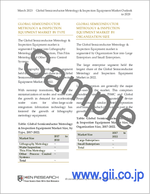
By Type
Lithography Metrology
Wafer Inspection
Thin Film Metrology
Other Process Control Systems
By Organization Size
Large Enterprises
Small Enterprises
By Geography
North America (USA, Canada, and Mexico)
Europe (Germany, UK, France, Spain, and Italy)
Asia Pacific (China, Japan, South Korea, India, Indonesia, and Australia)
LAMEA (Latin America, Middle East, and Africa)
Key Players
KLA Corporation
Applied Materials Inc.
Onto Innovation Inc.
Thermo Fisher Scientific Inc.
Hitachi High-Tech Corporation
Nova Ltd.
ASML Holding NV
Lasertec Corporation
JEOL Ltd.
Nikon Metrology NV
Camtek Limited
Unity Semiconductor SAS
Key Trends by Market Segment
By Type: The lithography metrology type segment held the largest market share in the Global Semiconductor Metrology and Inspection Equipment Market in 2021.
With nonstop transitions, such as the miniaturization of nodes and wafer sizes, the growth in demand for accelerating wafer sizes for ultra-large-scale integration fabrication technology has fostered the growth of lithography metrology equipment.
In addition, a critical dimension scanning electron microscope (CD-SEM) is used for measuring the dimensions of the patterns formed on the wafer; the device is used as part of the manufacturing lines of electronic instruments and devices. Presently, CD-SEM has been witnessing significant demand, owing to the semiconductor output process.
By Organization Size: The large enterprise segment held the largest share of the Global Semiconductor Metrology and Inspection Equipment Market in 2021.
Large enterprises are generally the major end-user of the market. This comprises foundries, similar to TSMC and Global Foundry, and integrated device manufacturers, similar to Intel Corporation and Samsung which play a major part in the growth of this segment.
In November 2021, Samsung Corporation declared to construct a semiconductor manufacturing unit in Texas due to the adding demand for chips for phones and other devices. The company planned to invest US$ 17 billion in constructing this unit. A significant part of that measure is anticipated to be employed for buying semiconductor metrology and inspection equipment. Similar strategic developments embraced by large enterprises are expected to drive the semiconductor metrology and inspection market growth for this segment.
By Geography: Asia Pacific accounted for the largest market share in 2021 within the total Global Semiconductor Metrology and Inspection Equipment Market.
The Asia Pacific is one of the prominent regions for the semiconductor industry regarding manufacturing and application. According to the Secretariat of Industrial Approvals (SIA), Asia Pacific is the largest indigenous semiconductor market, and China is the largest single-country market.
Additionally, in the region, the trend toward multiple-layer measurement is expanding due to the use of cluster deposition systems, where the lack of reality of single-layer measurement is driving the demand. Also, the fab manufacturers are shifting process monitors from bare wafers to production wafers due to the high cost and inspection challenges faced by the miniaturization of wafers.
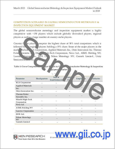
Competitive Landscape
The global semiconductor metrology and inspection equipment market is highly competitive with ~150 players which include globally diversified players, regional players as well as a large number of country-niche players.
Country-Niche players comprise the highest share of 50% total competitors which is followed by the regional players holding a 35% share. Some of the major players in the market include KLA Corporation, Applied Materials Inc., Onto Innovation Inc. Thermo Fisher Scientific Inc., Hitachi High-Tech Corporation, Nova Ltd., ASML Holding NV, Lasertec Corporation., JEOL Ltd.., Nikon Metrology NV, Camtek Limited., Unity Semiconductor SAS, and others.
Recent Developments Related to Major and Emerging Companies
In July 2022, Onto Innovation Inc., declared the launch of its innovative acoustic metrology products. The new Echo system further expands the transferable request for in-line characterization of opaque films, which is estimated to be roughly USD 110 million, by using the principle of picosecond ultrasonic to deliver critical thickness metrology and material characterization for crucial technology transitions in the DRAM and high- stack NAND memory markets.
In June 2022, Hitachi High-Tech Corporation declared the launch of the Hitachi Dark Field Wafer Defect Inspection System DI2800, a critical element in semiconductor manufacturers' metrology capabilities. The DI2800 is a high-speed metrology system designed to identify faults and particles on patterned wafers up to 8 inches (200 mm) in diameter. Its high output and performance can help assure device trust ability and safety, particularly for largely sensitive operations like the Internet of Things (IoT) and automotive fields where 100 inspections are needed.
Conclusion
The global semiconductor metrology and inspection equipment market is forecasted to continue a gradual growth that is witnessed during the forecast period. Key trends driving market expansion include the increasing demand for the miniaturization of electronic circuits in consumer electronic devices and rising industrial automation and widespread chip integration in the demand for the studied market. The market is highly competitive with ~150 participants concentrating on expansion strategies through product innovations as well as acquisitions and mergers.
Note: This is an On-Demand/Planned report, so the figures quoted here for a market size estimate, forecast, growth, segment share, and competitive landscape are based on initial findings and might vary slightly in the actual report. Also, any required customizations can be covered to the best feasible extent for Pre-booking clients, and the report delivered within a maximum of two working weeks.
Key Topics Covered in the Report
Snapshot of the Global Semiconductor Metrology and Inspection Equipment Market
Industry Value Chain and Ecosystem Analysis
Market size and Segmentation of the Global Semiconductor Metrology and Inspection Equipment Market
Historic Growth of the Overall Global Semiconductor Metrology and Inspection Equipment Market and Segments
Competition Scenario of the Market and Key Developments of Competitors
Porter's 5 Forces Analysis of the Global Semiconductor Metrology and Inspection Equipment Market
Overview, Product Offerings, and SWOT Analysis of Key Competitors
COVID-19 Impact on the Overall Global Semiconductor Metrology and Inspection Equipment Market
Future Market Forecast and Growth Rates of the Total Global Semiconductor Metrology and Inspection Equipment Market and by Segments
Market Size of Type / Organization Size Segments with Historical CAGR and Future Forecasts
Analysis of the Semiconductor Metrology and Inspection Equipment Market in Major Regions
Major Production / Consumption Hubs in the Major Regions
Major Country-wise Historic and Future Market Growth Rates of the Total Market and Segments
Overview of Notable Emerging Competitor Companies within Each Major Country
Major Players Mentioned in the report
KLA Corporation
Applied Materials Inc.
Onto Innovation Inc.
Thermo Fisher Scientific Inc.
Hitachi High-Tech Corporation
Nova Ltd.
ASML Holding NV
Lasertec Corporation
JEOL Ltd.
Nikon Metrology NV
Camtek Limited
Unity Semiconductor SAS
Notable Emerging Companies Mentioned in the Report
Advantest Corporation
Cadence Design Systems Inc.
GCT Semiconductor Inc.
Micross Silicon Turnkey Solutions
INNOPHASE
Key Target Audience - Organizations and Entities Who Can Benefit by Subscribing This Report
Metrology/Inspection Suppliers
Semiconductor Processing Companies
Semiconductor Manufacturers
Wafer Fabrication Companies
MOCVD Engineering Firms
Semiconductor Research and Development Institutes
Electronics Market Research & Consulting Firms
Banking and Financial Institutions focused on Semiconductor Industry
Semiconductor IP Suppliers
Semiconductor Chip Manufacturers
SoC and Hardware Suppliers
Government & Regulatory Authorities
PCB Designers and Manufacturers
Components and Material Suppliers for Semiconductor Inspection Equipment
Semiconductor Testing & Inspection Companies
Government Ministries and Departments of Electronics Industry
Time Period Captured in the Report
Historical Period: 2017-2021
Forecast Period: 2022E-2028F
Frequently Asked Questions
What is the Study Period of this Market Report?
The Global Semiconductor Metrology and Inspection Equipment Market is covered from 2017-2028 in this report, which includes a forecast for the period 2022E-2028F.
What is the Future Growth Rate of the Global Semiconductor Metrology and Inspection Equipment Market?
The Global Semiconductor Metrology and Inspection Equipment Market is expected to witness a CAGR of about 7% over the next six years.
What are the Key Factors Driving the Global Semiconductor Metrology and Inspection Equipment Market?
Key trends driving market expansion include increasing demand for the miniaturization of electronic circuits in consumer electronic devices and rising industrial automation, and widespread chip integration in the demand for the studied market.
Which is the Largest Type Segment within the Global Semiconductor Metrology and Inspection Equipment Market?
The lithography metrology type segment held the largest share of the Global Semiconductor Metrology and Inspection Equipment Market in 2021.
Who are the Key Players in Global Semiconductor Metrology and Inspection Equipment Market?
KLA Corporation, Applied Materials Inc., Onto Innovation Inc. Thermo Fisher Scientific Inc., Hitachi High-Tech Corporation, Nova Ltd., ASML Holding NV, Lasertec Corporation., JEOL Ltd.., Nikon Metrology NV, Camtek Limited., Unity Semiconductor SAS, among others are the major companies operating in Global Semiconductor Metrology and Inspection Equipment Market.
Table Of Contents
Scope:
1. Executive Summary
- 1.1 Highlights of Global Semiconductor Metrology and Inspection Equipment Market Historic Growth & Forecast
- 1.2 Highlights of Market Trends, Challenges, and Competition
- 1.3 Highlights of Market Revenue Share by Segments
2. Market Overview and Key Trends Impacting Growth
- 2.1 Global Semiconductor Metrology and Inspection Equipment Market Taxonomy
- 2.2 Industry Value Chain
- 2.3 The Ecosystem of Major Entities in the Global Semiconductor Metrology and Inspection Equipment Market
- 2.4 Government Regulations & Developments
- 2.5 Key Growth Drivers & Challenges Impacting the Market
- 2.6 COVID-19 Impact on Global Semiconductor Metrology and Inspection Equipment Market
- 2.7 Total Global Semiconductor Metrology and Inspection Equipment Market Historic Growth by Segment Type, 2017-2021
2.7.1 By Type
2.7.2 By Organization Size
2.7.3 By Regions
- 2.8 Total Global Semiconductor Metrology and Inspection Equipment Market Historic Growth and Forecast, 2017-2028
- 2.9 Key Takeaways
3. Global - Market Segmentation by Type, Historic Growth, Outlook & Forecasts
- 3.1 Market Definition - Segmentation by Type
- 3.2 Market Revenue Share, Historic Growth, Outlook, and Forecasts by Type, 2017-2028
3.2.1 Lithography Metrology
3.2.2 Wafer Inspection
3.2.3 Thin Film Metrology
3.2.4 Other Process Control Systems
- 3.3 Key Takeaways from Market Segmentation by Type
4. Global - Market Segmentation by Organization Size, Historic Growth, Outlook & Forecasts
- 4.1 Market Definition - Segmentation by Organization Size
- 4.2 Market Revenue Share, Historic Growth, Outlook, and Forecasts by Organization Size, 2017-2028
4.2.1 Large Enterprises
4.2.2 Small Enterprises
- 4.3 Key Takeaways from Market Segmentation by Organization Size
5. Industry / Competition Analysis - Competitive Landscape
- 5.1 Products of Players (Competitors) & Share of Competition
- 5.2 Porter's 5 Forces Analysis of Global Semiconductor Metrology and Inspection Equipment Competitors
- 5.3 Key Developments in the Global Semiconductor Metrology and Inspection Equipment Sector Impacting Market Growth
- 5.4 Comparison of Leading Competitors within the Global Semiconductor Metrology and Inspection Equipment Market, 2021
- 5.5 Comparison of Leading Competitors within the Global Semiconductor Metrology and Inspection Equipment Market by Coverage of Type, 2021
- 5.6 Comparison of Leading Competitors within the Global Semiconductor Metrology and Inspection Equipment Market by Coverage of Organization Size, 2021
- 5.7 Comparison of Leading Competitors within the Global Semiconductor Metrology and Inspection Equipment Market by Coverage of Regions, 2021
- 5.8 Key Takeaways from Competitive Landscape
6. Key Competitor Profiles (Company Overview, Product Offerings, SWOT Analysis)
- 6.1 KLA Corporation
- 6.2 Applied Materials Inc.
- 6.3 Onto Innovation Inc.
- 6.4 Thermo Fisher Scientific Inc.
- 6.5 Hitachi High-Tech Corporation
- 6.6 Nova Ltd.
- 6.7 ASML Holding NV
- 6.8 Lasertec Corporation
- 6.9 JEOL Ltd.
- 6.10 Nikon Metrology NV
- 6.11 Camtek Limited
- 6.12 Unity Semiconductor SAS
7. Geographic Analysis & Major Regions Market Historic Growth, Outlook, and Forecasts
- 7.1 Major Region Comparison of Macroeconomic Factors
- 7.2 Total Global- Market Revenue Share, Historic Growth, Outlook and Forecasts by Geography, 2017-2028
- 7.3 Major Region Market Analysis, Historic Growth, Outlook & Forecasts, 2017-2028
- 7.4 North America - Semiconductor Metrology and Inspection Equipment Market Analysis
7.4.1 Major Production and Consumption Hubs in North America
7.4.2 Notable Emerging Semiconductor Metrology and Inspection Equipment Companies in North America
7.4.3 Market Revenue Share, Historic Growth, Outlook, and Forecasts by Type, 2017-2028
7.4.4 Market Revenue Share, Historic Growth, Outlook, and Forecasts by Organization Size, 2017-2028
7.4.5 Market Revenue Share, Historic Growth, Outlook, and Forecasts by Major Countries, 2017-2028
7.4.5.1 USA
7.4.5.2 Canada
7.4.5.3 Mexico
- 7.5 Europe- Semiconductor Metrology and Inspection Equipment Market Analysis
7.5.1 Major Production and Consumption Hubs in Europe
7.5.2 Notable Emerging Semiconductor Metrology and Inspection Equipment Companies in Europe
7.5.3 Market Revenue Share, Historic Growth, Outlook, and Forecasts by Type, 2017-2028
7.5.4 Market Revenue Share, Historic Growth, Outlook, and Forecasts by Organization Size, 2017-2028
7.5.5 Market Revenue Share, Historic Growth, Outlook, and Forecasts by Country, 2017-2028
7.5.5.1 Germany
7.5.5.2 UK
7.5.5.3 France
7.5.5.4 Spain
7.5.5.5 Italy
7.5.5.6 Rest of Europe
- 7.6 Asia-Pacific- Semiconductor Metrology and Inspection Equipment Market Analysis
7.6.1 Major Production and Consumption Hubs in Asia-Pacific
7.6.2 Notable Emerging Semiconductor Metrology and Inspection Equipment Companies in Asia-Pacific
7.6.3 Market Revenue Share, Historic Growth, Outlook, and Forecasts by Type, 2017-2028
7.6.4 Market Revenue Share, Historic Growth, Outlook, and Forecasts by Organization Size, 2017-2028
7.6.5 Market Revenue Share, Historic Growth, Outlook, and Forecasts by Major Countries, 2017-2028
7.6.5.1 China
7.6.5.2 Japan
7.6.5.3 South Korea
7.6.5.4 India
7.6.5.5 Indonesia
7.6.5.6 Australia
7.6.5.7 Rest of Asia Pacific
- 7.7 LAMEA - Semiconductor Metrology and Inspection Equipment Market Analysis
7.7.1 Major Production and Consumption Hubs in LAMEA
7.7.2 Notable Emerging Semiconductor Metrology and Inspection Equipment Companies in LAMEA
7.7.3 Market Revenue Share, Historic Growth, Outlook, and Forecasts by Type, 2017-2028
7.7.4 Market Revenue Share, Historic Growth, Outlook, and Forecasts by Organization Size, 2017-2028
7.7.5 Market Revenue Share, Historic Growth, Outlook, and Forecasts by Major Sub-Regions, 2017-2028
7.7.5.1 Latin America
7.7.5.2 Middle East
7.7.5.3 Africa
8. Industry Expert's Opinions/Perspectives
- 8.1 Notable Statements/Quotes from Industry Experts and C-Level Executives on Current Status and Future Outlook of the Market
9. Analyst Recommendation
- 9.1 Analyst Recommendations on Identified Major Opportunities and Potential Strategies to Gain from Opportunities
10. Appendix
- 10.1 Research Methodology - Market Size Estimation, Forecast, and Sanity Check Approach
- 10.2 Sample Discussion Guide
Disclaimer