|
|
市場調査レポート
商品コード
1677277
TFLNフォトニックチップ鋳造市場:部品、技術、鋳造サービス、用途、エンドユーザー別-2025-2030年の世界予測TFLN Photonic Chip Foundry Market by Component, Technology, Foundry Services, Application, End-User - Global Forecast 2025-2030 |
||||||
|
|||||||
カスタマイズ可能
適宜更新あり
|
|||||||

| TFLNフォトニックチップ鋳造市場:部品、技術、鋳造サービス、用途、エンドユーザー別-2025-2030年の世界予測 |
|
出版日: 2025年03月09日
発行: 360iResearch
ページ情報: 英文 189 Pages
納期: 即日から翌営業日
|

全表示
- 概要
- 図表
- 目次
TFLNフォトニックチップ鋳造市場は、2024年には7億6,084万米ドルとなり、2025年には8億6,058万米ドル、CAGR13.39%で成長し、2030年には16億1,768万米ドルに達すると予測されています。
| 主な市場の統計 | |
|---|---|
| 基準年 2024 | 7億6,084万米ドル |
| 推定年 2025 | 8億6,058万米ドル |
| 予測年 2030 | 16億1,768万米ドル |
| CAGR(%) | 13.39% |
フォトニクスの分野は、技術の進歩が現代の電子アーキテクチャにおける光ベースのシステムの統合を再定義し、急速に進化しています。高速データ要件とエネルギー効率に対する要求の高まりに伴い、フォトニックチップ鋳造セクターは技術革新と拡大が急増しています。このイントロダクションでは、Thin-Film Lithium Niobate(TFLN)技術が提供する変革的能力と、次世代通信、センシング、コンピューティング・ソリューションにおけるその実現的役割について分析します。
近年、TFLNフォトニックチップは、その多様な性能と幅広い材料やアプリケーションとの互換性により、好ましいプラットフォームとして台頭してきました。フォトニックインテグレーションと材料科学の先駆的な調査により、メーカーは従来の限界を克服し、高性能でスケーラブルなデバイスを実現できるようになりました。このダイナミックな進化は、世界の研究開発への多額の投資によって支えられており、技術開発者、鋳造サービスプロバイダー、エンドユーザー部門間の協力の機会をもたらしています。
TFLNをフォトニックチップに統合することで、シグナルインテグリティの向上、歪みの低減、ひいては現代のデータセンター、自動車システム、ヘルスケア機器の機能を変革する大きな可能性が生まれます。このような急速な技術革新の中で、業界の主なプレーヤーは、TFLN固有の利点を活用するために、これまで以上に洗練された製造方法を開発しています。利害関係者は、技術革新が急務であると同時に飛躍的な成長が期待される市場において、どのように自らを位置づけるのが最善かを考えなければならないです。
TFLNフォトニックチップ鋳造市場の変革
過去10年間、TFLNフォトニックチップ市場は、業界標準を再定義するような一連の変革的変化を経験してきました。先進的な製造手法、統合技術、ハイブリッドシステムの進化が、総体として限界を押し広げ、堅牢な性能と精密なエンジニアリングが融合する環境を作り出してきました。
この進化の主な原動力のひとつは、異種・多機能統合の急速な採用です。このような技術の進歩は、従来の製造プロセスによる制約を超越し、より複雑で効率的なフォトニック回路の開発を可能にしています。例えば、ハイブリッドフォトニック回路は、エネルギー消費と信号精度を最適化しながら、異なる要素を統合したシステムです。このような技術を光ファイバー通信システムと連携させることで、飛躍的に大きなデータ負荷に対応できるデバイスの開発が可能になりました。
プラットフォームの製造技術も大幅に改良されました。メーカーは現在、工業規格に適合するだけでなく、それを上回るコンポーネントを製造するために、精密リソグラフィとエッチングに依存しています。プラットフォーム製造への新たな焦点は、かつては面倒でミスの起こりやすいプロセスであったものを、無駄がなく効率的で拡張性の高いプロセスへと変貌させつつあります。この変革は技術的な改善にとどまらず、フォトニックチップ鋳造のビジネスモデルにも及んでおり、自動化された高スループット生産設備への戦略的投資によって、コスト構造や市場参入戦略が再定義されています。
こうした変革的なシフトは、プロトタイピング、テスト、量産を改善する道を開いています。TFLN技術の進化は、革新的な集積戦略の採用とともに、フォトニックチップがかつてないレベルの性能と信頼性を特徴とする未来への舞台を整えたことは明らかです。その結果、業界の利害関係者は変化を受け入れ、これらの進歩を十分に活用するアジャイル手法と先進的な開発戦略を採用することが求められています。
複数の市場次元にわたる主要セグメンテーションの洞察
市場を詳細にセグメンテーションすることで、TFLNフォトニックチップの状況を形成している様々な側面についてニュアンスを持って理解する必要性が強調されます。分析により、部品設計、技術、サービス提供、アプリケーション、エンドユーザー需要など、市場動向に影響を与える重要な側面が明らかになります。
コンポーネントに基づく市場は、電気光学変調器、光アイソレータ、フォトニック集積回路、TFLNチップ、導波路などの製品範囲にわたって調査されています。これらの素子はフォトニックシステムのバックボーンを形成しており、それぞれが異なる機能を提供することでデバイスの性能を総合的に高めています。これらのコンポーネントの重視は、信号制御の強化と効率的なデータ処理の推進を反映しています。
技術面では、ヘテロジニアス&マルチファンクショナルインテグレーション、ハイブリッドフォトニックサーキット、光ファイバー通信、プラットフォームファブリケーション、精密リソグラフィ&エッチングの革新が業界を牽引しています。これらの技術カテゴリーは、動作フレームワークこそ異なるもの、待ち時間の短縮、処理能力の向上、部品統合の最適化という目標に収斂しています。このような技術の融合が最新のフォトニックシステムを支えており、商用・産業用を問わず様々なアプリケーションへの適応性を高めています。
鋳造サービスに基づいてさらに細分化すると、パッケージング、プロトタイピング、テスト&バリデーション、大量生産といった業務慣行の進化した役割が見えてくる。これらの各分野は、製品開発の各段階を通じて品質と信頼性が維持されることを保証するだけでなく、市場投入までの時間とコスト効率の面で競争力を生み出します。メーカーは、ますます高度化する生産サイクルの要求に応えるため、これらのプロセスを絶えず合理化しています。
アプリケーションの観点からは、バイオセンシング、環境モニタリング、量子コンピューティングに焦点を当てた市場が、多様な最終用途の可能性を示しています。これらのアプリケーションは、TFLNフォトニックチップ固有の高い精度と信頼性から恩恵を受けます。精度が最重要視される環境において、これらのデバイスは重要なブレークスルーを推進する能力を持っています。
最後に、エンドユーザー別の評価では、自動車、家電、データセンター、ヘルスケア、通信といった分野に焦点が当てられています。これらの産業は世界経済にとって重要であり、堅牢で高性能な通信およびセンシング・ソリューションを必要としています。これらの分野特有の要求や動作条件から、高い信頼性と効率を実現できるカスタマイズされたソリューションが必要とされ、TFLNフォトニックチップにおけるターゲットイノベーションの事例が強化されています。全体として、これらのセグメンテーションの洞察は、充実した新興国開拓と市場参入戦略を考案するために不可欠な、重層的な視点を提供しています。
目次
第1章 序文
第2章 調査手法
第3章 エグゼクティブサマリー
第4章 市場の概要
第5章 市場洞察
- 市場力学
- 促進要因
- テクノロジー業界では小型化の動向が高まっている
- データセンターと光インターコネクトの需要増加
- フォトニックチップ製造におけるイノベーションを促進する政府の支援と政策的インセンティブ
- 抑制要因
- 技術的な複雑さと高い製造コスト
- 機会
- 量子コンピューティングと通信の進歩
- 量子技術の応用拡大
- 課題
- 代替フォトニック材料との競合
- 促進要因
- 市場セグメンテーション分析
- コンポーネント:電気通信における電気光学変調器の採用の増加
- アプリケーション:バイオセンシングアプリケーションにおけるTFLNフォトニックチップ鋳造の適応
- ポーターのファイブフォース分析
- PESTEL分析
- 政治的
- 経済
- 社交
- 技術的
- 法律上
- 環境
第6章 TFLNフォトニックチップ鋳造市場:コンポーネント別
- 電気光学変調器
- 光アイソレータ
- フォトニック集積回路
- TFLNチップ
- 導波管
第7章 TFLNフォトニックチップ鋳造市場:技術別
- 異種および多機能統合
- ハイブリッド光回路
- 光ファイバー通信
- プラットフォーム製造
- 精密リソグラフィーとエッチング
第8章 TFLNフォトニックチップ鋳造市場ファウンドリーサービス
- パッケージ
- プロトタイピング
- テストと検証
- 大量生産
第9章 TFLNフォトニックチップ鋳造市場:用途別
- バイオセンシング
- 環境モニタリング
- 量子コンピューティング
第10章 TFLNフォトニックチップ鋳造市場:エンドユーザー別
- 自動車
- 家電
- データセンター
- ヘルスケア
- 通信
第11章 南北アメリカのTFLNフォトニックチップ鋳造市場
- アルゼンチン
- ブラジル
- カナダ
- メキシコ
- 米国
第12章 アジア太平洋地域のTFLNフォトニックチップ鋳造市場
- オーストラリア
- 中国
- インド
- インドネシア
- 日本
- マレーシア
- フィリピン
- シンガポール
- 韓国
- 台湾
- タイ
- ベトナム
第13章 欧州・中東・アフリカのTFLNフォトニックチップ鋳造市場
- デンマーク
- エジプト
- フィンランド
- フランス
- ドイツ
- イスラエル
- イタリア
- オランダ
- ナイジェリア
- ノルウェー
- ポーランド
- カタール
- ロシア
- サウジアラビア
- 南アフリカ
- スペイン
- スウェーデン
- スイス
- トルコ
- アラブ首長国連邦
- 英国
第14章 競合情勢
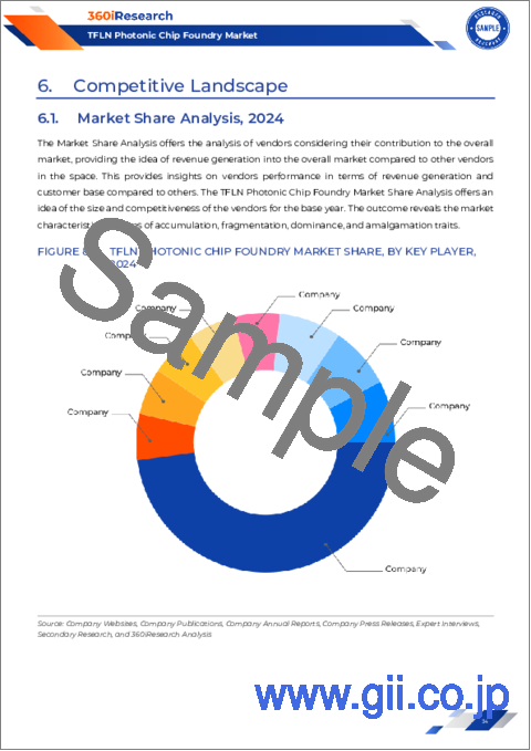
- 市場シェア分析, 2024
- FPNVポジショニングマトリックス, 2024
- 競合シナリオ分析
- 戦略分析と提言
企業一覧
- Advanced Fiber Resources Ltd
- CSEM Centre Suisse d'Electronique et de Microtechnique SA
- Fujitsu Limited
- HyperLight
- Infinera Corporation
- LIGENTEC SA
- Lightium AG
- LioniX International
- M2Optics, Inc.
- Ningbo ORI-CHIP Optoelectronics Technology Co. ltd.
- Q.ANT GmbH
- Quantum Computing, Inc.
- Silicon Austria Labs
- Tower Semiconductor
- ULVAC
LIST OF FIGURES
- FIGURE 1. TFLN PHOTONIC CHIP FOUNDRY MARKET MULTI-CURRENCY
- FIGURE 2. TFLN PHOTONIC CHIP FOUNDRY MARKET MULTI-LANGUAGE
- FIGURE 3. TFLN PHOTONIC CHIP FOUNDRY MARKET RESEARCH PROCESS
- FIGURE 4. TFLN PHOTONIC CHIP FOUNDRY MARKET SIZE, 2024 VS 2030
- FIGURE 5. GLOBAL TFLN PHOTONIC CHIP FOUNDRY MARKET SIZE, 2018-2030 (USD MILLION)
- FIGURE 6. GLOBAL TFLN PHOTONIC CHIP FOUNDRY MARKET SIZE, BY REGION, 2024 VS 2025 VS 2030 (USD MILLION)
- FIGURE 7. GLOBAL TFLN PHOTONIC CHIP FOUNDRY MARKET SIZE, BY COUNTRY, 2024 VS 2025 VS 2030 (USD MILLION)
- FIGURE 8. GLOBAL TFLN PHOTONIC CHIP FOUNDRY MARKET SIZE, BY COMPONENT, 2024 VS 2030 (%)
- FIGURE 9. GLOBAL TFLN PHOTONIC CHIP FOUNDRY MARKET SIZE, BY COMPONENT, 2024 VS 2025 VS 2030 (USD MILLION)
- FIGURE 10. GLOBAL TFLN PHOTONIC CHIP FOUNDRY MARKET SIZE, BY TECHNOLOGY, 2024 VS 2030 (%)
- FIGURE 11. GLOBAL TFLN PHOTONIC CHIP FOUNDRY MARKET SIZE, BY TECHNOLOGY, 2024 VS 2025 VS 2030 (USD MILLION)
- FIGURE 12. GLOBAL TFLN PHOTONIC CHIP FOUNDRY MARKET SIZE, BY FOUNDRY SERVICES, 2024 VS 2030 (%)
- FIGURE 13. GLOBAL TFLN PHOTONIC CHIP FOUNDRY MARKET SIZE, BY FOUNDRY SERVICES, 2024 VS 2025 VS 2030 (USD MILLION)
- FIGURE 14. GLOBAL TFLN PHOTONIC CHIP FOUNDRY MARKET SIZE, BY APPLICATION, 2024 VS 2030 (%)
- FIGURE 15. GLOBAL TFLN PHOTONIC CHIP FOUNDRY MARKET SIZE, BY APPLICATION, 2024 VS 2025 VS 2030 (USD MILLION)
- FIGURE 16. GLOBAL TFLN PHOTONIC CHIP FOUNDRY MARKET SIZE, BY END-USER, 2024 VS 2030 (%)
- FIGURE 17. GLOBAL TFLN PHOTONIC CHIP FOUNDRY MARKET SIZE, BY END-USER, 2024 VS 2025 VS 2030 (USD MILLION)
- FIGURE 18. AMERICAS TFLN PHOTONIC CHIP FOUNDRY MARKET SIZE, BY COUNTRY, 2024 VS 2030 (%)
- FIGURE 19. AMERICAS TFLN PHOTONIC CHIP FOUNDRY MARKET SIZE, BY COUNTRY, 2024 VS 2025 VS 2030 (USD MILLION)
- FIGURE 20. UNITED STATES TFLN PHOTONIC CHIP FOUNDRY MARKET SIZE, BY STATE, 2024 VS 2030 (%)
- FIGURE 21. UNITED STATES TFLN PHOTONIC CHIP FOUNDRY MARKET SIZE, BY STATE, 2024 VS 2025 VS 2030 (USD MILLION)
- FIGURE 22. ASIA-PACIFIC TFLN PHOTONIC CHIP FOUNDRY MARKET SIZE, BY COUNTRY, 2024 VS 2030 (%)
- FIGURE 23. ASIA-PACIFIC TFLN PHOTONIC CHIP FOUNDRY MARKET SIZE, BY COUNTRY, 2024 VS 2025 VS 2030 (USD MILLION)
- FIGURE 24. EUROPE, MIDDLE EAST & AFRICA TFLN PHOTONIC CHIP FOUNDRY MARKET SIZE, BY COUNTRY, 2024 VS 2030 (%)
- FIGURE 25. EUROPE, MIDDLE EAST & AFRICA TFLN PHOTONIC CHIP FOUNDRY MARKET SIZE, BY COUNTRY, 2024 VS 2025 VS 2030 (USD MILLION)
- FIGURE 26. TFLN PHOTONIC CHIP FOUNDRY MARKET SHARE, BY KEY PLAYER, 2024
- FIGURE 27. TFLN PHOTONIC CHIP FOUNDRY MARKET, FPNV POSITIONING MATRIX, 2024
LIST OF TABLES
- TABLE 1. TFLN PHOTONIC CHIP FOUNDRY MARKET SEGMENTATION & COVERAGE
- TABLE 2. UNITED STATES DOLLAR EXCHANGE RATE, 2018-2024
- TABLE 3. GLOBAL TFLN PHOTONIC CHIP FOUNDRY MARKET SIZE, 2018-2030 (USD MILLION)
- TABLE 4. GLOBAL TFLN PHOTONIC CHIP FOUNDRY MARKET SIZE, BY REGION, 2018-2030 (USD MILLION)
- TABLE 5. GLOBAL TFLN PHOTONIC CHIP FOUNDRY MARKET SIZE, BY COUNTRY, 2018-2030 (USD MILLION)
- TABLE 6. TFLN PHOTONIC CHIP FOUNDRY MARKET DYNAMICS
- TABLE 7. GLOBAL TFLN PHOTONIC CHIP FOUNDRY MARKET SIZE, BY COMPONENT, 2018-2030 (USD MILLION)
- TABLE 8. GLOBAL TFLN PHOTONIC CHIP FOUNDRY MARKET SIZE, BY ELECTRO-OPTIC MODULATORS, BY REGION, 2018-2030 (USD MILLION)
- TABLE 9. GLOBAL TFLN PHOTONIC CHIP FOUNDRY MARKET SIZE, BY OPTICAL ISOLATORS, BY REGION, 2018-2030 (USD MILLION)
- TABLE 10. GLOBAL TFLN PHOTONIC CHIP FOUNDRY MARKET SIZE, BY PHOTONIC INTEGRATED CIRCUITS, BY REGION, 2018-2030 (USD MILLION)
- TABLE 11. GLOBAL TFLN PHOTONIC CHIP FOUNDRY MARKET SIZE, BY TFLN CHIPS, BY REGION, 2018-2030 (USD MILLION)
- TABLE 12. GLOBAL TFLN PHOTONIC CHIP FOUNDRY MARKET SIZE, BY WAVEGUIDES, BY REGION, 2018-2030 (USD MILLION)
- TABLE 13. GLOBAL TFLN PHOTONIC CHIP FOUNDRY MARKET SIZE, BY TECHNOLOGY, 2018-2030 (USD MILLION)
- TABLE 14. GLOBAL TFLN PHOTONIC CHIP FOUNDRY MARKET SIZE, BY HETEROGENEOUS & MULTI-FUNCTIONAL INTEGRATION, BY REGION, 2018-2030 (USD MILLION)
- TABLE 15. GLOBAL TFLN PHOTONIC CHIP FOUNDRY MARKET SIZE, BY HYBRID PHOTONIC CIRCUITS, BY REGION, 2018-2030 (USD MILLION)
- TABLE 16. GLOBAL TFLN PHOTONIC CHIP FOUNDRY MARKET SIZE, BY OPTICAL FIBER COMMUNICATION, BY REGION, 2018-2030 (USD MILLION)
- TABLE 17. GLOBAL TFLN PHOTONIC CHIP FOUNDRY MARKET SIZE, BY PLATFORM FABRICATION, BY REGION, 2018-2030 (USD MILLION)
- TABLE 18. GLOBAL TFLN PHOTONIC CHIP FOUNDRY MARKET SIZE, BY PRECISION LITHOGRAPHY & ETCHING, BY REGION, 2018-2030 (USD MILLION)
- TABLE 19. GLOBAL TFLN PHOTONIC CHIP FOUNDRY MARKET SIZE, BY FOUNDRY SERVICES, 2018-2030 (USD MILLION)
- TABLE 20. GLOBAL TFLN PHOTONIC CHIP FOUNDRY MARKET SIZE, BY PACKAGING, BY REGION, 2018-2030 (USD MILLION)
- TABLE 21. GLOBAL TFLN PHOTONIC CHIP FOUNDRY MARKET SIZE, BY PROTOTYPING, BY REGION, 2018-2030 (USD MILLION)
- TABLE 22. GLOBAL TFLN PHOTONIC CHIP FOUNDRY MARKET SIZE, BY TESTING & VALIDATION, BY REGION, 2018-2030 (USD MILLION)
- TABLE 23. GLOBAL TFLN PHOTONIC CHIP FOUNDRY MARKET SIZE, BY VOLUME PRODUCTION, BY REGION, 2018-2030 (USD MILLION)
- TABLE 24. GLOBAL TFLN PHOTONIC CHIP FOUNDRY MARKET SIZE, BY APPLICATION, 2018-2030 (USD MILLION)
- TABLE 25. GLOBAL TFLN PHOTONIC CHIP FOUNDRY MARKET SIZE, BY BIOSENSING, BY REGION, 2018-2030 (USD MILLION)
- TABLE 26. GLOBAL TFLN PHOTONIC CHIP FOUNDRY MARKET SIZE, BY ENVIRONMENTAL MONITORING, BY REGION, 2018-2030 (USD MILLION)
- TABLE 27. GLOBAL TFLN PHOTONIC CHIP FOUNDRY MARKET SIZE, BY QUANTUM COMPUTING, BY REGION, 2018-2030 (USD MILLION)
- TABLE 28. GLOBAL TFLN PHOTONIC CHIP FOUNDRY MARKET SIZE, BY END-USER, 2018-2030 (USD MILLION)
- TABLE 29. GLOBAL TFLN PHOTONIC CHIP FOUNDRY MARKET SIZE, BY AUTOMOTIVE, BY REGION, 2018-2030 (USD MILLION)
- TABLE 30. GLOBAL TFLN PHOTONIC CHIP FOUNDRY MARKET SIZE, BY CONSUMER ELECTRONICS, BY REGION, 2018-2030 (USD MILLION)
- TABLE 31. GLOBAL TFLN PHOTONIC CHIP FOUNDRY MARKET SIZE, BY DATA CENTERS, BY REGION, 2018-2030 (USD MILLION)
- TABLE 32. GLOBAL TFLN PHOTONIC CHIP FOUNDRY MARKET SIZE, BY HEALTHCARE, BY REGION, 2018-2030 (USD MILLION)
- TABLE 33. GLOBAL TFLN PHOTONIC CHIP FOUNDRY MARKET SIZE, BY TELECOMMUNICATIONS, BY REGION, 2018-2030 (USD MILLION)
- TABLE 34. AMERICAS TFLN PHOTONIC CHIP FOUNDRY MARKET SIZE, BY COMPONENT, 2018-2030 (USD MILLION)
- TABLE 35. AMERICAS TFLN PHOTONIC CHIP FOUNDRY MARKET SIZE, BY TECHNOLOGY, 2018-2030 (USD MILLION)
- TABLE 36. AMERICAS TFLN PHOTONIC CHIP FOUNDRY MARKET SIZE, BY FOUNDRY SERVICES, 2018-2030 (USD MILLION)
- TABLE 37. AMERICAS TFLN PHOTONIC CHIP FOUNDRY MARKET SIZE, BY APPLICATION, 2018-2030 (USD MILLION)
- TABLE 38. AMERICAS TFLN PHOTONIC CHIP FOUNDRY MARKET SIZE, BY END-USER, 2018-2030 (USD MILLION)
- TABLE 39. AMERICAS TFLN PHOTONIC CHIP FOUNDRY MARKET SIZE, BY COUNTRY, 2018-2030 (USD MILLION)
- TABLE 40. ARGENTINA TFLN PHOTONIC CHIP FOUNDRY MARKET SIZE, BY COMPONENT, 2018-2030 (USD MILLION)
- TABLE 41. ARGENTINA TFLN PHOTONIC CHIP FOUNDRY MARKET SIZE, BY TECHNOLOGY, 2018-2030 (USD MILLION)
- TABLE 42. ARGENTINA TFLN PHOTONIC CHIP FOUNDRY MARKET SIZE, BY FOUNDRY SERVICES, 2018-2030 (USD MILLION)
- TABLE 43. ARGENTINA TFLN PHOTONIC CHIP FOUNDRY MARKET SIZE, BY APPLICATION, 2018-2030 (USD MILLION)
- TABLE 44. ARGENTINA TFLN PHOTONIC CHIP FOUNDRY MARKET SIZE, BY END-USER, 2018-2030 (USD MILLION)
- TABLE 45. BRAZIL TFLN PHOTONIC CHIP FOUNDRY MARKET SIZE, BY COMPONENT, 2018-2030 (USD MILLION)
- TABLE 46. BRAZIL TFLN PHOTONIC CHIP FOUNDRY MARKET SIZE, BY TECHNOLOGY, 2018-2030 (USD MILLION)
- TABLE 47. BRAZIL TFLN PHOTONIC CHIP FOUNDRY MARKET SIZE, BY FOUNDRY SERVICES, 2018-2030 (USD MILLION)
- TABLE 48. BRAZIL TFLN PHOTONIC CHIP FOUNDRY MARKET SIZE, BY APPLICATION, 2018-2030 (USD MILLION)
- TABLE 49. BRAZIL TFLN PHOTONIC CHIP FOUNDRY MARKET SIZE, BY END-USER, 2018-2030 (USD MILLION)
- TABLE 50. CANADA TFLN PHOTONIC CHIP FOUNDRY MARKET SIZE, BY COMPONENT, 2018-2030 (USD MILLION)
- TABLE 51. CANADA TFLN PHOTONIC CHIP FOUNDRY MARKET SIZE, BY TECHNOLOGY, 2018-2030 (USD MILLION)
- TABLE 52. CANADA TFLN PHOTONIC CHIP FOUNDRY MARKET SIZE, BY FOUNDRY SERVICES, 2018-2030 (USD MILLION)
- TABLE 53. CANADA TFLN PHOTONIC CHIP FOUNDRY MARKET SIZE, BY APPLICATION, 2018-2030 (USD MILLION)
- TABLE 54. CANADA TFLN PHOTONIC CHIP FOUNDRY MARKET SIZE, BY END-USER, 2018-2030 (USD MILLION)
- TABLE 55. MEXICO TFLN PHOTONIC CHIP FOUNDRY MARKET SIZE, BY COMPONENT, 2018-2030 (USD MILLION)
- TABLE 56. MEXICO TFLN PHOTONIC CHIP FOUNDRY MARKET SIZE, BY TECHNOLOGY, 2018-2030 (USD MILLION)
- TABLE 57. MEXICO TFLN PHOTONIC CHIP FOUNDRY MARKET SIZE, BY FOUNDRY SERVICES, 2018-2030 (USD MILLION)
- TABLE 58. MEXICO TFLN PHOTONIC CHIP FOUNDRY MARKET SIZE, BY APPLICATION, 2018-2030 (USD MILLION)
- TABLE 59. MEXICO TFLN PHOTONIC CHIP FOUNDRY MARKET SIZE, BY END-USER, 2018-2030 (USD MILLION)
- TABLE 60. UNITED STATES TFLN PHOTONIC CHIP FOUNDRY MARKET SIZE, BY COMPONENT, 2018-2030 (USD MILLION)
- TABLE 61. UNITED STATES TFLN PHOTONIC CHIP FOUNDRY MARKET SIZE, BY TECHNOLOGY, 2018-2030 (USD MILLION)
- TABLE 62. UNITED STATES TFLN PHOTONIC CHIP FOUNDRY MARKET SIZE, BY FOUNDRY SERVICES, 2018-2030 (USD MILLION)
- TABLE 63. UNITED STATES TFLN PHOTONIC CHIP FOUNDRY MARKET SIZE, BY APPLICATION, 2018-2030 (USD MILLION)
- TABLE 64. UNITED STATES TFLN PHOTONIC CHIP FOUNDRY MARKET SIZE, BY END-USER, 2018-2030 (USD MILLION)
- TABLE 65. UNITED STATES TFLN PHOTONIC CHIP FOUNDRY MARKET SIZE, BY STATE, 2018-2030 (USD MILLION)
- TABLE 66. ASIA-PACIFIC TFLN PHOTONIC CHIP FOUNDRY MARKET SIZE, BY COMPONENT, 2018-2030 (USD MILLION)
- TABLE 67. ASIA-PACIFIC TFLN PHOTONIC CHIP FOUNDRY MARKET SIZE, BY TECHNOLOGY, 2018-2030 (USD MILLION)
- TABLE 68. ASIA-PACIFIC TFLN PHOTONIC CHIP FOUNDRY MARKET SIZE, BY FOUNDRY SERVICES, 2018-2030 (USD MILLION)
- TABLE 69. ASIA-PACIFIC TFLN PHOTONIC CHIP FOUNDRY MARKET SIZE, BY APPLICATION, 2018-2030 (USD MILLION)
- TABLE 70. ASIA-PACIFIC TFLN PHOTONIC CHIP FOUNDRY MARKET SIZE, BY END-USER, 2018-2030 (USD MILLION)
- TABLE 71. ASIA-PACIFIC TFLN PHOTONIC CHIP FOUNDRY MARKET SIZE, BY COUNTRY, 2018-2030 (USD MILLION)
- TABLE 72. AUSTRALIA TFLN PHOTONIC CHIP FOUNDRY MARKET SIZE, BY COMPONENT, 2018-2030 (USD MILLION)
- TABLE 73. AUSTRALIA TFLN PHOTONIC CHIP FOUNDRY MARKET SIZE, BY TECHNOLOGY, 2018-2030 (USD MILLION)
- TABLE 74. AUSTRALIA TFLN PHOTONIC CHIP FOUNDRY MARKET SIZE, BY FOUNDRY SERVICES, 2018-2030 (USD MILLION)
- TABLE 75. AUSTRALIA TFLN PHOTONIC CHIP FOUNDRY MARKET SIZE, BY APPLICATION, 2018-2030 (USD MILLION)
- TABLE 76. AUSTRALIA TFLN PHOTONIC CHIP FOUNDRY MARKET SIZE, BY END-USER, 2018-2030 (USD MILLION)
- TABLE 77. CHINA TFLN PHOTONIC CHIP FOUNDRY MARKET SIZE, BY COMPONENT, 2018-2030 (USD MILLION)
- TABLE 78. CHINA TFLN PHOTONIC CHIP FOUNDRY MARKET SIZE, BY TECHNOLOGY, 2018-2030 (USD MILLION)
- TABLE 79. CHINA TFLN PHOTONIC CHIP FOUNDRY MARKET SIZE, BY FOUNDRY SERVICES, 2018-2030 (USD MILLION)
- TABLE 80. CHINA TFLN PHOTONIC CHIP FOUNDRY MARKET SIZE, BY APPLICATION, 2018-2030 (USD MILLION)
- TABLE 81. CHINA TFLN PHOTONIC CHIP FOUNDRY MARKET SIZE, BY END-USER, 2018-2030 (USD MILLION)
- TABLE 82. INDIA TFLN PHOTONIC CHIP FOUNDRY MARKET SIZE, BY COMPONENT, 2018-2030 (USD MILLION)
- TABLE 83. INDIA TFLN PHOTONIC CHIP FOUNDRY MARKET SIZE, BY TECHNOLOGY, 2018-2030 (USD MILLION)
- TABLE 84. INDIA TFLN PHOTONIC CHIP FOUNDRY MARKET SIZE, BY FOUNDRY SERVICES, 2018-2030 (USD MILLION)
- TABLE 85. INDIA TFLN PHOTONIC CHIP FOUNDRY MARKET SIZE, BY APPLICATION, 2018-2030 (USD MILLION)
- TABLE 86. INDIA TFLN PHOTONIC CHIP FOUNDRY MARKET SIZE, BY END-USER, 2018-2030 (USD MILLION)
- TABLE 87. INDONESIA TFLN PHOTONIC CHIP FOUNDRY MARKET SIZE, BY COMPONENT, 2018-2030 (USD MILLION)
- TABLE 88. INDONESIA TFLN PHOTONIC CHIP FOUNDRY MARKET SIZE, BY TECHNOLOGY, 2018-2030 (USD MILLION)
- TABLE 89. INDONESIA TFLN PHOTONIC CHIP FOUNDRY MARKET SIZE, BY FOUNDRY SERVICES, 2018-2030 (USD MILLION)
- TABLE 90. INDONESIA TFLN PHOTONIC CHIP FOUNDRY MARKET SIZE, BY APPLICATION, 2018-2030 (USD MILLION)
- TABLE 91. INDONESIA TFLN PHOTONIC CHIP FOUNDRY MARKET SIZE, BY END-USER, 2018-2030 (USD MILLION)
- TABLE 92. JAPAN TFLN PHOTONIC CHIP FOUNDRY MARKET SIZE, BY COMPONENT, 2018-2030 (USD MILLION)
- TABLE 93. JAPAN TFLN PHOTONIC CHIP FOUNDRY MARKET SIZE, BY TECHNOLOGY, 2018-2030 (USD MILLION)
- TABLE 94. JAPAN TFLN PHOTONIC CHIP FOUNDRY MARKET SIZE, BY FOUNDRY SERVICES, 2018-2030 (USD MILLION)
- TABLE 95. JAPAN TFLN PHOTONIC CHIP FOUNDRY MARKET SIZE, BY APPLICATION, 2018-2030 (USD MILLION)
- TABLE 96. JAPAN TFLN PHOTONIC CHIP FOUNDRY MARKET SIZE, BY END-USER, 2018-2030 (USD MILLION)
- TABLE 97. MALAYSIA TFLN PHOTONIC CHIP FOUNDRY MARKET SIZE, BY COMPONENT, 2018-2030 (USD MILLION)
- TABLE 98. MALAYSIA TFLN PHOTONIC CHIP FOUNDRY MARKET SIZE, BY TECHNOLOGY, 2018-2030 (USD MILLION)
- TABLE 99. MALAYSIA TFLN PHOTONIC CHIP FOUNDRY MARKET SIZE, BY FOUNDRY SERVICES, 2018-2030 (USD MILLION)
- TABLE 100. MALAYSIA TFLN PHOTONIC CHIP FOUNDRY MARKET SIZE, BY APPLICATION, 2018-2030 (USD MILLION)
- TABLE 101. MALAYSIA TFLN PHOTONIC CHIP FOUNDRY MARKET SIZE, BY END-USER, 2018-2030 (USD MILLION)
- TABLE 102. PHILIPPINES TFLN PHOTONIC CHIP FOUNDRY MARKET SIZE, BY COMPONENT, 2018-2030 (USD MILLION)
- TABLE 103. PHILIPPINES TFLN PHOTONIC CHIP FOUNDRY MARKET SIZE, BY TECHNOLOGY, 2018-2030 (USD MILLION)
- TABLE 104. PHILIPPINES TFLN PHOTONIC CHIP FOUNDRY MARKET SIZE, BY FOUNDRY SERVICES, 2018-2030 (USD MILLION)
- TABLE 105. PHILIPPINES TFLN PHOTONIC CHIP FOUNDRY MARKET SIZE, BY APPLICATION, 2018-2030 (USD MILLION)
- TABLE 106. PHILIPPINES TFLN PHOTONIC CHIP FOUNDRY MARKET SIZE, BY END-USER, 2018-2030 (USD MILLION)
- TABLE 107. SINGAPORE TFLN PHOTONIC CHIP FOUNDRY MARKET SIZE, BY COMPONENT, 2018-2030 (USD MILLION)
- TABLE 108. SINGAPORE TFLN PHOTONIC CHIP FOUNDRY MARKET SIZE, BY TECHNOLOGY, 2018-2030 (USD MILLION)
- TABLE 109. SINGAPORE TFLN PHOTONIC CHIP FOUNDRY MARKET SIZE, BY FOUNDRY SERVICES, 2018-2030 (USD MILLION)
- TABLE 110. SINGAPORE TFLN PHOTONIC CHIP FOUNDRY MARKET SIZE, BY APPLICATION, 2018-2030 (USD MILLION)
- TABLE 111. SINGAPORE TFLN PHOTONIC CHIP FOUNDRY MARKET SIZE, BY END-USER, 2018-2030 (USD MILLION)
- TABLE 112. SOUTH KOREA TFLN PHOTONIC CHIP FOUNDRY MARKET SIZE, BY COMPONENT, 2018-2030 (USD MILLION)
- TABLE 113. SOUTH KOREA TFLN PHOTONIC CHIP FOUNDRY MARKET SIZE, BY TECHNOLOGY, 2018-2030 (USD MILLION)
- TABLE 114. SOUTH KOREA TFLN PHOTONIC CHIP FOUNDRY MARKET SIZE, BY FOUNDRY SERVICES, 2018-2030 (USD MILLION)
- TABLE 115. SOUTH KOREA TFLN PHOTONIC CHIP FOUNDRY MARKET SIZE, BY APPLICATION, 2018-2030 (USD MILLION)
- TABLE 116. SOUTH KOREA TFLN PHOTONIC CHIP FOUNDRY MARKET SIZE, BY END-USER, 2018-2030 (USD MILLION)
- TABLE 117. TAIWAN TFLN PHOTONIC CHIP FOUNDRY MARKET SIZE, BY COMPONENT, 2018-2030 (USD MILLION)
- TABLE 118. TAIWAN TFLN PHOTONIC CHIP FOUNDRY MARKET SIZE, BY TECHNOLOGY, 2018-2030 (USD MILLION)
- TABLE 119. TAIWAN TFLN PHOTONIC CHIP FOUNDRY MARKET SIZE, BY FOUNDRY SERVICES, 2018-2030 (USD MILLION)
- TABLE 120. TAIWAN TFLN PHOTONIC CHIP FOUNDRY MARKET SIZE, BY APPLICATION, 2018-2030 (USD MILLION)
- TABLE 121. TAIWAN TFLN PHOTONIC CHIP FOUNDRY MARKET SIZE, BY END-USER, 2018-2030 (USD MILLION)
- TABLE 122. THAILAND TFLN PHOTONIC CHIP FOUNDRY MARKET SIZE, BY COMPONENT, 2018-2030 (USD MILLION)
- TABLE 123. THAILAND TFLN PHOTONIC CHIP FOUNDRY MARKET SIZE, BY TECHNOLOGY, 2018-2030 (USD MILLION)
- TABLE 124. THAILAND TFLN PHOTONIC CHIP FOUNDRY MARKET SIZE, BY FOUNDRY SERVICES, 2018-2030 (USD MILLION)
- TABLE 125. THAILAND TFLN PHOTONIC CHIP FOUNDRY MARKET SIZE, BY APPLICATION, 2018-2030 (USD MILLION)
- TABLE 126. THAILAND TFLN PHOTONIC CHIP FOUNDRY MARKET SIZE, BY END-USER, 2018-2030 (USD MILLION)
- TABLE 127. VIETNAM TFLN PHOTONIC CHIP FOUNDRY MARKET SIZE, BY COMPONENT, 2018-2030 (USD MILLION)
- TABLE 128. VIETNAM TFLN PHOTONIC CHIP FOUNDRY MARKET SIZE, BY TECHNOLOGY, 2018-2030 (USD MILLION)
- TABLE 129. VIETNAM TFLN PHOTONIC CHIP FOUNDRY MARKET SIZE, BY FOUNDRY SERVICES, 2018-2030 (USD MILLION)
- TABLE 130. VIETNAM TFLN PHOTONIC CHIP FOUNDRY MARKET SIZE, BY APPLICATION, 2018-2030 (USD MILLION)
- TABLE 131. VIETNAM TFLN PHOTONIC CHIP FOUNDRY MARKET SIZE, BY END-USER, 2018-2030 (USD MILLION)
- TABLE 132. EUROPE, MIDDLE EAST & AFRICA TFLN PHOTONIC CHIP FOUNDRY MARKET SIZE, BY COMPONENT, 2018-2030 (USD MILLION)
- TABLE 133. EUROPE, MIDDLE EAST & AFRICA TFLN PHOTONIC CHIP FOUNDRY MARKET SIZE, BY TECHNOLOGY, 2018-2030 (USD MILLION)
- TABLE 134. EUROPE, MIDDLE EAST & AFRICA TFLN PHOTONIC CHIP FOUNDRY MARKET SIZE, BY FOUNDRY SERVICES, 2018-2030 (USD MILLION)
- TABLE 135. EUROPE, MIDDLE EAST & AFRICA TFLN PHOTONIC CHIP FOUNDRY MARKET SIZE, BY APPLICATION, 2018-2030 (USD MILLION)
- TABLE 136. EUROPE, MIDDLE EAST & AFRICA TFLN PHOTONIC CHIP FOUNDRY MARKET SIZE, BY END-USER, 2018-2030 (USD MILLION)
- TABLE 137. EUROPE, MIDDLE EAST & AFRICA TFLN PHOTONIC CHIP FOUNDRY MARKET SIZE, BY COUNTRY, 2018-2030 (USD MILLION)
- TABLE 138. DENMARK TFLN PHOTONIC CHIP FOUNDRY MARKET SIZE, BY COMPONENT, 2018-2030 (USD MILLION)
- TABLE 139. DENMARK TFLN PHOTONIC CHIP FOUNDRY MARKET SIZE, BY TECHNOLOGY, 2018-2030 (USD MILLION)
- TABLE 140. DENMARK TFLN PHOTONIC CHIP FOUNDRY MARKET SIZE, BY FOUNDRY SERVICES, 2018-2030 (USD MILLION)
- TABLE 141. DENMARK TFLN PHOTONIC CHIP FOUNDRY MARKET SIZE, BY APPLICATION, 2018-2030 (USD MILLION)
- TABLE 142. DENMARK TFLN PHOTONIC CHIP FOUNDRY MARKET SIZE, BY END-USER, 2018-2030 (USD MILLION)
- TABLE 143. EGYPT TFLN PHOTONIC CHIP FOUNDRY MARKET SIZE, BY COMPONENT, 2018-2030 (USD MILLION)
- TABLE 144. EGYPT TFLN PHOTONIC CHIP FOUNDRY MARKET SIZE, BY TECHNOLOGY, 2018-2030 (USD MILLION)
- TABLE 145. EGYPT TFLN PHOTONIC CHIP FOUNDRY MARKET SIZE, BY FOUNDRY SERVICES, 2018-2030 (USD MILLION)
- TABLE 146. EGYPT TFLN PHOTONIC CHIP FOUNDRY MARKET SIZE, BY APPLICATION, 2018-2030 (USD MILLION)
- TABLE 147. EGYPT TFLN PHOTONIC CHIP FOUNDRY MARKET SIZE, BY END-USER, 2018-2030 (USD MILLION)
- TABLE 148. FINLAND TFLN PHOTONIC CHIP FOUNDRY MARKET SIZE, BY COMPONENT, 2018-2030 (USD MILLION)
- TABLE 149. FINLAND TFLN PHOTONIC CHIP FOUNDRY MARKET SIZE, BY TECHNOLOGY, 2018-2030 (USD MILLION)
- TABLE 150. FINLAND TFLN PHOTONIC CHIP FOUNDRY MARKET SIZE, BY FOUNDRY SERVICES, 2018-2030 (USD MILLION)
- TABLE 151. FINLAND TFLN PHOTONIC CHIP FOUNDRY MARKET SIZE, BY APPLICATION, 2018-2030 (USD MILLION)
- TABLE 152. FINLAND TFLN PHOTONIC CHIP FOUNDRY MARKET SIZE, BY END-USER, 2018-2030 (USD MILLION)
- TABLE 153. FRANCE TFLN PHOTONIC CHIP FOUNDRY MARKET SIZE, BY COMPONENT, 2018-2030 (USD MILLION)
- TABLE 154. FRANCE TFLN PHOTONIC CHIP FOUNDRY MARKET SIZE, BY TECHNOLOGY, 2018-2030 (USD MILLION)
- TABLE 155. FRANCE TFLN PHOTONIC CHIP FOUNDRY MARKET SIZE, BY FOUNDRY SERVICES, 2018-2030 (USD MILLION)
- TABLE 156. FRANCE TFLN PHOTONIC CHIP FOUNDRY MARKET SIZE, BY APPLICATION, 2018-2030 (USD MILLION)
- TABLE 157. FRANCE TFLN PHOTONIC CHIP FOUNDRY MARKET SIZE, BY END-USER, 2018-2030 (USD MILLION)
- TABLE 158. GERMANY TFLN PHOTONIC CHIP FOUNDRY MARKET SIZE, BY COMPONENT, 2018-2030 (USD MILLION)
- TABLE 159. GERMANY TFLN PHOTONIC CHIP FOUNDRY MARKET SIZE, BY TECHNOLOGY, 2018-2030 (USD MILLION)
- TABLE 160. GERMANY TFLN PHOTONIC CHIP FOUNDRY MARKET SIZE, BY FOUNDRY SERVICES, 2018-2030 (USD MILLION)
- TABLE 161. GERMANY TFLN PHOTONIC CHIP FOUNDRY MARKET SIZE, BY APPLICATION, 2018-2030 (USD MILLION)
- TABLE 162. GERMANY TFLN PHOTONIC CHIP FOUNDRY MARKET SIZE, BY END-USER, 2018-2030 (USD MILLION)
- TABLE 163. ISRAEL TFLN PHOTONIC CHIP FOUNDRY MARKET SIZE, BY COMPONENT, 2018-2030 (USD MILLION)
- TABLE 164. ISRAEL TFLN PHOTONIC CHIP FOUNDRY MARKET SIZE, BY TECHNOLOGY, 2018-2030 (USD MILLION)
- TABLE 165. ISRAEL TFLN PHOTONIC CHIP FOUNDRY MARKET SIZE, BY FOUNDRY SERVICES, 2018-2030 (USD MILLION)
- TABLE 166. ISRAEL TFLN PHOTONIC CHIP FOUNDRY MARKET SIZE, BY APPLICATION, 2018-2030 (USD MILLION)
- TABLE 167. ISRAEL TFLN PHOTONIC CHIP FOUNDRY MARKET SIZE, BY END-USER, 2018-2030 (USD MILLION)
- TABLE 168. ITALY TFLN PHOTONIC CHIP FOUNDRY MARKET SIZE, BY COMPONENT, 2018-2030 (USD MILLION)
- TABLE 169. ITALY TFLN PHOTONIC CHIP FOUNDRY MARKET SIZE, BY TECHNOLOGY, 2018-2030 (USD MILLION)
- TABLE 170. ITALY TFLN PHOTONIC CHIP FOUNDRY MARKET SIZE, BY FOUNDRY SERVICES, 2018-2030 (USD MILLION)
- TABLE 171. ITALY TFLN PHOTONIC CHIP FOUNDRY MARKET SIZE, BY APPLICATION, 2018-2030 (USD MILLION)
- TABLE 172. ITALY TFLN PHOTONIC CHIP FOUNDRY MARKET SIZE, BY END-USER, 2018-2030 (USD MILLION)
- TABLE 173. NETHERLANDS TFLN PHOTONIC CHIP FOUNDRY MARKET SIZE, BY COMPONENT, 2018-2030 (USD MILLION)
- TABLE 174. NETHERLANDS TFLN PHOTONIC CHIP FOUNDRY MARKET SIZE, BY TECHNOLOGY, 2018-2030 (USD MILLION)
- TABLE 175. NETHERLANDS TFLN PHOTONIC CHIP FOUNDRY MARKET SIZE, BY FOUNDRY SERVICES, 2018-2030 (USD MILLION)
- TABLE 176. NETHERLANDS TFLN PHOTONIC CHIP FOUNDRY MARKET SIZE, BY APPLICATION, 2018-2030 (USD MILLION)
- TABLE 177. NETHERLANDS TFLN PHOTONIC CHIP FOUNDRY MARKET SIZE, BY END-USER, 2018-2030 (USD MILLION)
- TABLE 178. NIGERIA TFLN PHOTONIC CHIP FOUNDRY MARKET SIZE, BY COMPONENT, 2018-2030 (USD MILLION)
- TABLE 179. NIGERIA TFLN PHOTONIC CHIP FOUNDRY MARKET SIZE, BY TECHNOLOGY, 2018-2030 (USD MILLION)
- TABLE 180. NIGERIA TFLN PHOTONIC CHIP FOUNDRY MARKET SIZE, BY FOUNDRY SERVICES, 2018-2030 (USD MILLION)
- TABLE 181. NIGERIA TFLN PHOTONIC CHIP FOUNDRY MARKET SIZE, BY APPLICATION, 2018-2030 (USD MILLION)
- TABLE 182. NIGERIA TFLN PHOTONIC CHIP FOUNDRY MARKET SIZE, BY END-USER, 2018-2030 (USD MILLION)
- TABLE 183. NORWAY TFLN PHOTONIC CHIP FOUNDRY MARKET SIZE, BY COMPONENT, 2018-2030 (USD MILLION)
- TABLE 184. NORWAY TFLN PHOTONIC CHIP FOUNDRY MARKET SIZE, BY TECHNOLOGY, 2018-2030 (USD MILLION)
- TABLE 185. NORWAY TFLN PHOTONIC CHIP FOUNDRY MARKET SIZE, BY FOUNDRY SERVICES, 2018-2030 (USD MILLION)
- TABLE 186. NORWAY TFLN PHOTONIC CHIP FOUNDRY MARKET SIZE, BY APPLICATION, 2018-2030 (USD MILLION)
- TABLE 187. NORWAY TFLN PHOTONIC CHIP FOUNDRY MARKET SIZE, BY END-USER, 2018-2030 (USD MILLION)
- TABLE 188. POLAND TFLN PHOTONIC CHIP FOUNDRY MARKET SIZE, BY COMPONENT, 2018-2030 (USD MILLION)
- TABLE 189. POLAND TFLN PHOTONIC CHIP FOUNDRY MARKET SIZE, BY TECHNOLOGY, 2018-2030 (USD MILLION)
- TABLE 190. POLAND TFLN PHOTONIC CHIP FOUNDRY MARKET SIZE, BY FOUNDRY SERVICES, 2018-2030 (USD MILLION)
- TABLE 191. POLAND TFLN PHOTONIC CHIP FOUNDRY MARKET SIZE, BY APPLICATION, 2018-2030 (USD MILLION)
- TABLE 192. POLAND TFLN PHOTONIC CHIP FOUNDRY MARKET SIZE, BY END-USER, 2018-2030 (USD MILLION)
- TABLE 193. QATAR TFLN PHOTONIC CHIP FOUNDRY MARKET SIZE, BY COMPONENT, 2018-2030 (USD MILLION)
- TABLE 194. QATAR TFLN PHOTONIC CHIP FOUNDRY MARKET SIZE, BY TECHNOLOGY, 2018-2030 (USD MILLION)
- TABLE 195. QATAR TFLN PHOTONIC CHIP FOUNDRY MARKET SIZE, BY FOUNDRY SERVICES, 2018-2030 (USD MILLION)
- TABLE 196. QATAR TFLN PHOTONIC CHIP FOUNDRY MARKET SIZE, BY APPLICATION, 2018-2030 (USD MILLION)
- TABLE 197. QATAR TFLN PHOTONIC CHIP FOUNDRY MARKET SIZE, BY END-USER, 2018-2030 (USD MILLION)
- TABLE 198. RUSSIA TFLN PHOTONIC CHIP FOUNDRY MARKET SIZE, BY COMPONENT, 2018-2030 (USD MILLION)
- TABLE 199. RUSSIA TFLN PHOTONIC CHIP FOUNDRY MARKET SIZE, BY TECHNOLOGY, 2018-2030 (USD MILLION)
- TABLE 200. RUSSIA TFLN PHOTONIC CHIP FOUNDRY MARKET SIZE, BY FOUNDRY SERVICES, 2018-2030 (USD MILLION)
- TABLE 201. RUSSIA TFLN PHOTONIC CHIP FOUNDRY MARKET SIZE, BY APPLICATION, 2018-2030 (USD MILLION)
- TABLE 202. RUSSIA TFLN PHOTONIC CHIP FOUNDRY MARKET SIZE, BY END-USER, 2018-2030 (USD MILLION)
- TABLE 203. SAUDI ARABIA TFLN PHOTONIC CHIP FOUNDRY MARKET SIZE, BY COMPONENT, 2018-2030 (USD MILLION)
- TABLE 204. SAUDI ARABIA TFLN PHOTONIC CHIP FOUNDRY MARKET SIZE, BY TECHNOLOGY, 2018-2030 (USD MILLION)
- TABLE 205. SAUDI ARABIA TFLN PHOTONIC CHIP FOUNDRY MARKET SIZE, BY FOUNDRY SERVICES, 2018-2030 (USD MILLION)
- TABLE 206. SAUDI ARABIA TFLN PHOTONIC CHIP FOUNDRY MARKET SIZE, BY APPLICATION, 2018-2030 (USD MILLION)
- TABLE 207. SAUDI ARABIA TFLN PHOTONIC CHIP FOUNDRY MARKET SIZE, BY END-USER, 2018-2030 (USD MILLION)
- TABLE 208. SOUTH AFRICA TFLN PHOTONIC CHIP FOUNDRY MARKET SIZE, BY COMPONENT, 2018-2030 (USD MILLION)
- TABLE 209. SOUTH AFRICA TFLN PHOTONIC CHIP FOUNDRY MARKET SIZE, BY TECHNOLOGY, 2018-2030 (USD MILLION)
- TABLE 210. SOUTH AFRICA TFLN PHOTONIC CHIP FOUNDRY MARKET SIZE, BY FOUNDRY SERVICES, 2018-2030 (USD MILLION)
- TABLE 211. SOUTH AFRICA TFLN PHOTONIC CHIP FOUNDRY MARKET SIZE, BY APPLICATION, 2018-2030 (USD MILLION)
- TABLE 212. SOUTH AFRICA TFLN PHOTONIC CHIP FOUNDRY MARKET SIZE, BY END-USER, 2018-2030 (USD MILLION)
- TABLE 213. SPAIN TFLN PHOTONIC CHIP FOUNDRY MARKET SIZE, BY COMPONENT, 2018-2030 (USD MILLION)
- TABLE 214. SPAIN TFLN PHOTONIC CHIP FOUNDRY MARKET SIZE, BY TECHNOLOGY, 2018-2030 (USD MILLION)
- TABLE 215. SPAIN TFLN PHOTONIC CHIP FOUNDRY MARKET SIZE, BY FOUNDRY SERVICES, 2018-2030 (USD MILLION)
- TABLE 216. SPAIN TFLN PHOTONIC CHIP FOUNDRY MARKET SIZE, BY APPLICATION, 2018-2030 (USD MILLION)
- TABLE 217. SPAIN TFLN PHOTONIC CHIP FOUNDRY MARKET SIZE, BY END-USER, 2018-2030 (USD MILLION)
- TABLE 218. SWEDEN TFLN PHOTONIC CHIP FOUNDRY MARKET SIZE, BY COMPONENT, 2018-2030 (USD MILLION)
- TABLE 219. SWEDEN TFLN PHOTONIC CHIP FOUNDRY MARKET SIZE, BY TECHNOLOGY, 2018-2030 (USD MILLION)
- TABLE 220. SWEDEN TFLN PHOTONIC CHIP FOUNDRY MARKET SIZE, BY FOUNDRY SERVICES, 2018-2030 (USD MILLION)
- TABLE 221. SWEDEN TFLN PHOTONIC CHIP FOUNDRY MARKET SIZE, BY APPLICATION, 2018-2030 (USD MILLION)
- TABLE 222. SWEDEN TFLN PHOTONIC CHIP FOUNDRY MARKET SIZE, BY END-USER, 2018-2030 (USD MILLION)
- TABLE 223. SWITZERLAND TFLN PHOTONIC CHIP FOUNDRY MARKET SIZE, BY COMPONENT, 2018-2030 (USD MILLION)
- TABLE 224. SWITZERLAND TFLN PHOTONIC CHIP FOUNDRY MARKET SIZE, BY TECHNOLOGY, 2018-2030 (USD MILLION)
- TABLE 225. SWITZERLAND TFLN PHOTONIC CHIP FOUNDRY MARKET SIZE, BY FOUNDRY SERVICES, 2018-2030 (USD MILLION)
- TABLE 226. SWITZERLAND TFLN PHOTONIC CHIP FOUNDRY MARKET SIZE, BY APPLICATION, 2018-2030 (USD MILLION)
- TABLE 227. SWITZERLAND TFLN PHOTONIC CHIP FOUNDRY MARKET SIZE, BY END-USER, 2018-2030 (USD MILLION)
- TABLE 228. TURKEY TFLN PHOTONIC CHIP FOUNDRY MARKET SIZE, BY COMPONENT, 2018-2030 (USD MILLION)
- TABLE 229. TURKEY TFLN PHOTONIC CHIP FOUNDRY MARKET SIZE, BY TECHNOLOGY, 2018-2030 (USD MILLION)
- TABLE 230. TURKEY TFLN PHOTONIC CHIP FOUNDRY MARKET SIZE, BY FOUNDRY SERVICES, 2018-2030 (USD MILLION)
- TABLE 231. TURKEY TFLN PHOTONIC CHIP FOUNDRY MARKET SIZE, BY APPLICATION, 2018-2030 (USD MILLION)
- TABLE 232. TURKEY TFLN PHOTONIC CHIP FOUNDRY MARKET SIZE, BY END-USER, 2018-2030 (USD MILLION)
- TABLE 233. UNITED ARAB EMIRATES TFLN PHOTONIC CHIP FOUNDRY MARKET SIZE, BY COMPONENT, 2018-2030 (USD MILLION)
- TABLE 234. UNITED ARAB EMIRATES TFLN PHOTONIC CHIP FOUNDRY MARKET SIZE, BY TECHNOLOGY, 2018-2030 (USD MILLION)
- TABLE 235. UNITED ARAB EMIRATES TFLN PHOTONIC CHIP FOUNDRY MARKET SIZE, BY FOUNDRY SERVICES, 2018-2030 (USD MILLION)
- TABLE 236. UNITED ARAB EMIRATES TFLN PHOTONIC CHIP FOUNDRY MARKET SIZE, BY APPLICATION, 2018-2030 (USD MILLION)
- TABLE 237. UNITED ARAB EMIRATES TFLN PHOTONIC CHIP FOUNDRY MARKET SIZE, BY END-USER, 2018-2030 (USD MILLION)
- TABLE 238. UNITED KINGDOM TFLN PHOTONIC CHIP FOUNDRY MARKET SIZE, BY COMPONENT, 2018-2030 (USD MILLION)
- TABLE 239. UNITED KINGDOM TFLN PHOTONIC CHIP FOUNDRY MARKET SIZE, BY TECHNOLOGY, 2018-2030 (USD MILLION)
- TABLE 240. UNITED KINGDOM TFLN PHOTONIC CHIP FOUNDRY MARKET SIZE, BY FOUNDRY SERVICES, 2018-2030 (USD MILLION)
- TABLE 241. UNITED KINGDOM TFLN PHOTONIC CHIP FOUNDRY MARKET SIZE, BY APPLICATION, 2018-2030 (USD MILLION)
- TABLE 242. UNITED KINGDOM TFLN PHOTONIC CHIP FOUNDRY MARKET SIZE, BY END-USER, 2018-2030 (USD MILLION)
- TABLE 243. TFLN PHOTONIC CHIP FOUNDRY MARKET SHARE, BY KEY PLAYER, 2024
- TABLE 244. TFLN PHOTONIC CHIP FOUNDRY MARKET, FPNV POSITIONING MATRIX, 2024
The TFLN Photonic Chip Foundry Market was valued at USD 760.84 million in 2024 and is projected to grow to USD 860.58 million in 2025, with a CAGR of 13.39%, reaching USD 1,617.68 million by 2030.
| KEY MARKET STATISTICS | |
|---|---|
| Base Year [2024] | USD 760.84 million |
| Estimated Year [2025] | USD 860.58 million |
| Forecast Year [2030] | USD 1,617.68 million |
| CAGR (%) | 13.39% |
The field of photonics is rapidly evolving as technological advancements redefine the integration of light-based systems within modern electronic architectures. With high-speed data requirements and an increasing demand for energy efficiency, the photonic chip foundry sector is experiencing a surge in innovation and expansion. This introductory section provides an analysis of the transformative capabilities offered by Thin-Film Lithium Niobate (TFLN) technology and its enabling role in next-generation communication, sensing, and computing solutions.
In recent years, TFLN photonic chips have emerged as a preferred platform due to their versatility in performance and compatibility with a wide range of materials and applications. Pioneering research in photonic integration and material science has allowed manufacturers to overcome traditional limitations, thereby enabling devices that are both high-performing and scalable. This dynamic evolution is supported by substantial investments in research and development worldwide, ushering in opportunities for collaboration among technology developers, foundry service providers, and end-user sectors.
The integration of TFLN into photonic chips creates significant potential to improve signal integrity, reduce distortion, and ultimately transform the way modern data centers, automotive systems, and healthcare devices function. In this environment of rapid technological change, key players in the industry are developing ever more sophisticated fabrication methods to leverage the inherent benefits of TFLN. Stakeholders across the board must consider how to best position themselves in a market where innovation is both an imperative and a promise for exponential growth.
Transformative Shifts in the Photonic Chip Landscape
Over the past decade, the TFLN photonic chip market has observed a series of transformative shifts that have redefined industry standards. Advanced production methodologies, integration techniques, and the evolution of hybrid systems have collectively pushed the envelope, creating an environment where robust performance meets precision engineering.
One of the primary drivers of this evolution is the rapid adoption of heterogeneous and multi-functional integration. These technological advances have transcended the limitations imposed by traditional manufacturing processes, enabling more complex and efficient photonic circuits to be developed. Hybrid photonic circuits, for instance, integrate differing elements into a unified system while optimizing energy consumption and signal accuracy. The coordination of such technologies with optical fiber communication systems has allowed for the development of devices that can handle exponentially greater data loads.
Platform fabrication techniques have also undergone significant refinement. Manufacturers now rely on precision lithography and etching to produce components that not only meet but exceed industrial standards. The renewed focus on platform fabrication is transforming what was once a cumbersome and error-prone process into one that is lean, efficient, and highly scalable. This transformation is not limited to technical improvements but extends to the business models of photonic chip foundries, where strategic investments in automated, high-throughput production facilities have redefined cost structures and market entry strategies.
These transformative shifts are paving the way for improved prototyping, testing, and volume production. It is clear that the evolution of TFLN technology, along with the adoption of innovative integration strategies, has set the stage for a future where the photonic chip landscape will be characterized by unprecedented levels of performance and reliability. Consequently, industry stakeholders are called to embrace change, adopting agile methodologies and forward-thinking development strategies that leverage these advancements fully.
Key Segmentation Insights Across Multiple Market Dimensions
A detailed segmentation of the market underscores the necessity for a nuanced understanding of the various facets shaping the TFLN photonic chip landscape. Analysis reveals critical dimensions that influence market trends, including component design, technology, service provisions, applications, and end-user demands.
The market based on component is studied across a range of products such as Electro-Optic Modulators, Optical Isolators, Photonic Integrated Circuits, TFLN Chips, and Waveguides. These elements form the backbone of photonic systems, each contributing distinct functionalities that collectively enhance device performance. The emphasis on these components reflects a drive towards enhanced signal control and efficient data processing.
In terms of technology, the industry is propelled by innovations in Heterogeneous & Multi-Functional Integration, Hybrid Photonic Circuits, Optical Fiber Communication, Platform Fabrication, and Precision Lithography & Etching. These technological categories differ in their operational frameworks yet converge on the goal of reducing latency, boosting processing power, and optimizing component integration. This confluence of technologies underpins modern photonic systems, making them more adaptable to varied applications in both commercial and industrial settings.
Further segmentation based on foundry services brings to light the evolving roles of operational practices like Packaging, Prototyping, Testing & Validation, and Volume Production. Each of these facets not only ensures that quality and reliability are maintained through every phase of product development but also creates a competitive edge in terms of time-to-market and cost efficiency. Manufacturers are continually streamlining these processes to meet the demands of increasingly sophisticated production cycles.
From an application perspective, markets focused on Biosensing, Environmental Monitoring, and Quantum Computing offer a window into the diverse potential end uses. These applications benefit from the high level of precision and reliability inherent in TFLN photonic chips, which are critical for delivering accurate and actionable data. In environments where precision is paramount, these devices have the capability to drive significant breakthroughs.
Finally, an assessment based on the end-user reveals a focus on sectors such as Automotive, Consumer Electronics, Data Centers, Healthcare, and Telecommunications. These industries are critical to the global economy and require robust, high-performance communication and sensing solutions. The specific demands and operating conditions in these sectors necessitate tailored solutions capable of delivering high reliability and efficiency, reinforcing the case for targeted innovation in TFLN photonic chips. Overall, these segmentation insights provide a layered perspective that is essential for devising well-rounded development and market entry strategies.
Based on Component, market is studied across Electro-Optic Modulators, Optical Isolators, Photonic Integrated Circuits, TFLN Chips, and Waveguides.
Based on Technology, market is studied across Heterogeneous & Multi-Functional Integration, Hybrid Photonic Circuits, Optical Fiber Communication, Platform Fabrication, and Precision Lithography & Etching.
Based on Foundry Services, market is studied across Packaging, Prototyping, Testing & Validation, and Volume Production.
Based on Application, market is studied across Biosensing, Environmental Monitoring, and Quantum Computing.
Based on End-User, market is studied across Automotive, Consumer Electronics, Data Centers, Healthcare, and Telecommunications.
Key Regional Trends and Strategic Market Dynamics
Geographical dynamics play a pivotal role in shaping the global TFLN photonic chip market. Analyzing regions such as the Americas, Europe, Middle East & Africa, and Asia-Pacific provides critical insights into unique trends and growth drivers influenced by regional economic conditions, technological readiness, and infrastructural development.
The region of the Americas is known for its robust integration of advanced manufacturing techniques and high research intensity. With a longstanding history of innovation in optical communications, this region remains at the forefront of adopting TFLN-based technologies. Research institutions and technology centers in this area create a constant influx of novel ideas and breakthrough developments that translate into competitive advantages on the global stage.
In contrast, the region comprising Europe, the Middle East & Africa offers a diverse landscape characterized by strong governmental support for innovation and a keen focus on sustainability and energy efficiency. Here, a balanced mix of established technological giants and agile startups drives progress in photonic integration. These regions leverage a blend of strategic investments and collaborative research to foster an environment conducive to breakthrough developments, positioning themselves as key players in the photonic chip ecosystem.
Asia-Pacific is emerging as a dynamic focal point due to its rapid industrialization, burgeoning consumer market, and significant manufacturing capabilities. The extensive adoption of cutting-edge production techniques, coupled with increasing investments in research and development, is propelling this region into a leadership role in TFLN photonic chip production. Given its scale and fast-paced market dynamics, Asia-Pacific is not only a vital production hub but also serves as an indicator of global trends, reflecting the shifting paradigm towards integrated photonics and high-speed optical systems.
Collectively, these regional insights reveal how distinct economic, technological, and regulatory environments contribute to the evolution of the TFLN photonic chip market. A region-specific understanding is indispensable for stakeholders seeking to tailor their strategies and capitalize on local opportunities while responding to global industry trends.
Based on Region, market is studied across Americas, Asia-Pacific, and Europe, Middle East & Africa. The Americas is further studied across Argentina, Brazil, Canada, Mexico, and United States. The United States is further studied across California, Florida, Illinois, New York, Ohio, Pennsylvania, and Texas. The Asia-Pacific is further studied across Australia, China, India, Indonesia, Japan, Malaysia, Philippines, Singapore, South Korea, Taiwan, Thailand, and Vietnam. The Europe, Middle East & Africa is further studied across Denmark, Egypt, Finland, France, Germany, Israel, Italy, Netherlands, Nigeria, Norway, Poland, Qatar, Russia, Saudi Arabia, South Africa, Spain, Sweden, Switzerland, Turkey, United Arab Emirates, and United Kingdom.
Key Company Insights and Market Leadership Dynamics
Driving innovation and setting industry benchmarks are leading companies that have carved distinct niches in the TFLN photonic chip market. An analysis of key players reveals an ecosystem enriched with collaboration, technology leadership, and strategic investments, where each entity contributes uniquely to the development of the field.
For instance, Advanced Fiber Resources Ltd and CSEM Centre Suisse d'Electronique et de Microtechnique SA have distinguished themselves through their research-intensive approaches and unwavering commitment to quality. These organizations leverage cutting-edge technologies to refine manufacturing processes and set industry standards in precision and reliability. Similarly, Fujitsu Limited and HyperLight have played pivotal roles in advancing photonic systems by integrating next-generation design techniques with robust production methodologies.
Infinera Corporation and LIGENTEC SA are recognized for their significant contributions to developing scalable solutions that support high data throughput requirements in emerging telecommunications infrastructures. Lightium AG, LioniX International, and M2Optics, Inc. have also emerged as key innovators, transforming the landscape with their specialized expertise in system integration and component reliability. Ningbo ORI-CHIP Optoelectronics Technology Co. ltd. continues to make strides in harnessing the potential of TFLN technology, while Q.ANT GmbH and Quantum Computing, Inc. are at the forefront in confidence-inspiring claims regarding quantum computing applications and beyond.
Further, Silicon Austria Labs, Tower Semiconductor, and ULVAC have developed a reputation for excellence in advanced fabrication methodologies and precision engineering. Their investments in state-of-the-art production facilities have not only improved yield rates but have also enabled the delivery of high-efficiency photonic chips that meet the stringent requirements of modern data transmission and sensing applications.
The landscape shaped by these companies reflects a competitive culture where innovation is the primary currency. Their relentless drive towards operational excellence and market differentiation stands as a testament to the maturity and potential of the TFLN photonic chip market. This competitive interplay ensures that the industry remains vigorous, responsive, and continually adaptive to new technological challenges and opportunities.
The report delves into recent significant developments in the TFLN Photonic Chip Foundry Market, highlighting leading vendors and their innovative profiles. These include Advanced Fiber Resources Ltd, CSEM Centre Suisse d'Electronique et de Microtechnique SA, Fujitsu Limited, HyperLight, Infinera Corporation, LIGENTEC SA, Lightium AG, LioniX International, M2Optics, Inc., Ningbo ORI-CHIP Optoelectronics Technology Co. ltd., Q.ANT GmbH, Quantum Computing, Inc., Silicon Austria Labs, Tower Semiconductor, and ULVAC. Actionable Recommendations for Industry Leaders
Industry leaders are positioned to capitalize on the transformative potential of TFLN photonic chip technology by adopting several actionable strategies that align with current market dynamics and future trends. Foremost, prioritizing investments in advanced manufacturing and precision fabrication will yield long-term competitive advantages, as both production quality and efficiency are paramount in meeting growing market demands.
Stakeholders must focus on fostering collaborative research and development initiatives. By leveraging partnerships across academic institutions, technology firms, and manufacturing specialists, companies can accelerate innovation and reduce time-to-market for new products. Embracing a culture of continuous improvement will also drive process optimization, ensuring that operational practices remain aligned with evolving industry standards.
Diversification is another key strategy. Firms should consider expanding their portfolio by integrating various technologies such as heterogeneous integration and hybrid photonic circuits to enhance performance and create robust, multi-functional products. This diversification is especially important in an industry where the convergence of different technological fields creates new opportunities for innovation and differentiation.
Moreover, companies must pay close attention to market segmentation insights to tailor their strategies according to specific application areas and unique end-user requirements. Customized solutions that address the specialized needs of sectors such as automotive, healthcare, and data centers will secure higher market adoption and open new revenue streams. Investment in comprehensive testing, validation, and scaling up volume production procedures will be critical for maintaining quality while meeting demand.
Finally, it is advisable for industry leaders to maintain a forward-looking perspective on regional trends. Expanding operations to strategic markets, including the Americas, Europe, Middle East & Africa, and Asia-Pacific, will not only bolster market presence but also facilitate access to emerging technological ecosystems and new customer bases. The emphasis should be on building agile operational frameworks that can quickly adapt to shifting market conditions, thereby minimizing risk and maximizing growth potential.
Implementing these recommendations with a commitment to operational excellence will empower industry leaders to navigate a competitive landscape and secure a leadership position in the dynamic arena of TFLN photonic chip technology.
Conclusion - Summarizing the Evolution and Future Pathways
The dynamic landscape of TFLN photonic chip production is marked by rapid technological innovation, diverse market segmentation, and significant regional opportunities. The relentless pursuit of precision, efficiency, and integration has redefined the photonic chip space, setting the stage for transformative impacts across multiple sectors.
This analysis underscores how advancements in component design, fabrication techniques, and hybrid integration are setting new performance benchmarks. By understanding segmentation based on components, technology, foundry services, applications, and end-user bases, stakeholders can make informed decisions aimed at capturing emerging opportunities. The interplay of these segmentation factors with regional trends in the Americas, Europe, Middle East & Africa, and Asia-Pacific provides a strategic framework for both market expansion and focused innovation.
Moreover, key industry players have demonstrated that robust research, collaborative dynamics, and strategic investments are indispensable for leading market shifts. The competitive landscape, enriched by contributions from top-tier companies, reinforces the continuously evolving nature of the market. As the photonic chip foundry space matures, embracing forward-thinking technology and robust collaboration will remain critical to success.
In summary, the evolution of TFLN photonic chips is not simply a reflection of technological progress but also a harbinger of new market paradigms. Future pathways are driven by innovation, diversification, and strategic expansion across global regions. This comprehensive outlook equips decision-makers with the insights needed to navigate complexities and seize the opportunities inherent in this transformative field.
Table of Contents
1. Preface
- 1.1. Objectives of the Study
- 1.2. Market Segmentation & Coverage
- 1.3. Years Considered for the Study
- 1.4. Currency & Pricing
- 1.5. Language
- 1.6. Stakeholders
2. Research Methodology
- 2.1. Define: Research Objective
- 2.2. Determine: Research Design
- 2.3. Prepare: Research Instrument
- 2.4. Collect: Data Source
- 2.5. Analyze: Data Interpretation
- 2.6. Formulate: Data Verification
- 2.7. Publish: Research Report
- 2.8. Repeat: Report Update
3. Executive Summary
4. Market Overview
5. Market Insights
- 5.1. Market Dynamics
- 5.1.1. Drivers
- 5.1.1.1. Increasing miniaturization trends in the tech industry
- 5.1.1.2. Growing demand for data centers & optical interconnects
- 5.1.1.3. Government support and policy incentives fostering innovation in photonic chip manufacturing
- 5.1.2. Restraints
- 5.1.2.1. Technical complexities & high manufacturing costs
- 5.1.3. Opportunities
- 5.1.3.1. Advancements in quantum computing and communications
- 5.1.3.2. Expanding applications in quantum technologies
- 5.1.4. Challenges
- 5.1.4.1. Competition from alternative photonic materials
- 5.1.1. Drivers
- 5.2. Market Segmentation Analysis
- 5.2.1. Component: Increasing adoption of electro-optic modulators in telecommunications
- 5.2.2. Application: Adaption of TFLN photonic chip foundry in biosensing applications
- 5.3. Porter's Five Forces Analysis
- 5.3.1. Threat of New Entrants
- 5.3.2. Threat of Substitutes
- 5.3.3. Bargaining Power of Customers
- 5.3.4. Bargaining Power of Suppliers
- 5.3.5. Industry Rivalry
- 5.4. PESTLE Analysis
- 5.4.1. Political
- 5.4.2. Economic
- 5.4.3. Social
- 5.4.4. Technological
- 5.4.5. Legal
- 5.4.6. Environmental
6. TFLN Photonic Chip Foundry Market, by Component
- 6.1. Introduction
- 6.2. Electro-Optic Modulators
- 6.3. Optical Isolators
- 6.4. Photonic Integrated Circuits
- 6.5. TFLN Chips
- 6.6. Waveguides
7. TFLN Photonic Chip Foundry Market, by Technology
- 7.1. Introduction
- 7.2. Heterogeneous & Multi-Functional Integration
- 7.3. Hybrid Photonic Circuits
- 7.4. Optical Fiber Communication
- 7.5. Platform Fabrication
- 7.6. Precision Lithography & Etching
8. TFLN Photonic Chip Foundry Market, by Foundry Services
- 8.1. Introduction
- 8.2. Packaging
- 8.3. Prototyping
- 8.4. Testing & Validation
- 8.5. Volume Production
9. TFLN Photonic Chip Foundry Market, by Application
- 9.1. Introduction
- 9.2. Biosensing
- 9.3. Environmental Monitoring
- 9.4. Quantum Computing
10. TFLN Photonic Chip Foundry Market, by End-User
- 10.1. Introduction
- 10.2. Automotive
- 10.3. Consumer Electronics
- 10.4. Data Centers
- 10.5. Healthcare
- 10.6. Telecommunications
11. Americas TFLN Photonic Chip Foundry Market
- 11.1. Introduction
- 11.2. Argentina
- 11.3. Brazil
- 11.4. Canada
- 11.5. Mexico
- 11.6. United States
12. Asia-Pacific TFLN Photonic Chip Foundry Market
- 12.1. Introduction
- 12.2. Australia
- 12.3. China
- 12.4. India
- 12.5. Indonesia
- 12.6. Japan
- 12.7. Malaysia
- 12.8. Philippines
- 12.9. Singapore
- 12.10. South Korea
- 12.11. Taiwan
- 12.12. Thailand
- 12.13. Vietnam
13. Europe, Middle East & Africa TFLN Photonic Chip Foundry Market
- 13.1. Introduction
- 13.2. Denmark
- 13.3. Egypt
- 13.4. Finland
- 13.5. France
- 13.6. Germany
- 13.7. Israel
- 13.8. Italy
- 13.9. Netherlands
- 13.10. Nigeria
- 13.11. Norway
- 13.12. Poland
- 13.13. Qatar
- 13.14. Russia
- 13.15. Saudi Arabia
- 13.16. South Africa
- 13.17. Spain
- 13.18. Sweden
- 13.19. Switzerland
- 13.20. Turkey
- 13.21. United Arab Emirates
- 13.22. United Kingdom
14. Competitive Landscape
- 14.1. Market Share Analysis, 2024
- 14.2. FPNV Positioning Matrix, 2024
- 14.3. Competitive Scenario Analysis
- 14.3.1. Quantum Computing Inc. expands into high-demand TFLN photonic chip market with first major order
- 14.3.2. HyperLight secures USD 37 million in series B to accelerate TFLN photonics innovation for AI and telecom sectors
- 14.3.3. Lightium's USD 7 million seed funding accelerates TFLN photonic chip innovation to tackle AI-driven data center surge
- 14.4. Strategy Analysis & Recommendation
Companies Mentioned
- 1. Advanced Fiber Resources Ltd
- 2. CSEM Centre Suisse d'Electronique et de Microtechnique SA
- 3. Fujitsu Limited
- 4. HyperLight
- 5. Infinera Corporation
- 6. LIGENTEC SA
- 7. Lightium AG
- 8. LioniX International
- 9. M2Optics, Inc.
- 10. Ningbo ORI-CHIP Optoelectronics Technology Co. ltd.
- 11. Q.ANT GmbH
- 12. Quantum Computing, Inc.
- 13. Silicon Austria Labs
- 14. Tower Semiconductor
- 15. ULVAC
