プラズマエッチング:市場分析と戦略課題
Plasma Etching: Market Analysis and Strategic Issues- 発行日
- ページ情報
- 英文
- 納期
- 2~3営業日
- 商品コード
- 1479761
- 翻訳ツール提供対象 PDF対応AI翻訳ツールの無料貸し出しサービスのご利用が可能です
- 電子部品/半導体関連専門 電子部品/半導体関連専門を専門とする市場調査会社です。
概要
半導体製造における重要なプロセスである半導体プラズマエッチングは、業界の進化する要求、技術的進歩、市場力学を反映する多くの要因によって推進されています。
ムーアの法則の絶え間ない追求と、より小さく、より強力な半導体デバイスの需要に伴い、機能サイズを縮小し、デバイス密度を高める必要性が絶えず生じています。プラズマエッチングは、ナノメートル単位での精密なパターン転写を可能にし、高精度で高度な半導体構造の製造を容易にします。
FinFET、3D NANDフラッシュメモリ、多層配線など、半導体デバイスはますます複雑なアーキテクチャへと進化しており、望ましいデバイス形状と機能を実現するためには高度なエッチング技術が必要です。プラズマエッチングは、多層・多寸法の複雑なデバイス構造のパターニングに必要な柔軟性と制御性を提供します。
半導体材料が多様化し、化合物半導体デバイスが脚光を浴びるにつれ、高い選択性と均一性を維持しながら、さまざまな材料を効果的にエッチングできるプラズマエッチングプロセスに対するニーズが高まっています。特殊なエッチングケミストリーとプロセスレシピを開発することで、材料除去率と側壁プロファイルを精密に制御し、最適なデバイス性能と信頼性を確保することができます。
5Gワイヤレス通信、人工知能(AI)、モノのインターネット(IoT)、自律走行車など、新たな用途や技術の普及により、特定の性能特性や機能を備えた半導体デバイスの需要が高まっています。プラズマエッチングは、これらの用途の要件を満たすためにデバイス構造のカスタマイズと最適化を可能にし、新たな市場機会を切り開き、半導体製造の技術革新を促進します。
半導体産業は競争が激しく、各メーカーは市場シェア、技術的リーダーシップ、イノベーションを競っています。プラズマエッチング装置、材料、プロセス技術の絶え間ない進歩は、激しい市場競争によってもたらされ、進化する顧客の要求に応え、競争上の優位性を獲得するために、エッチング能力と性能の限界を押し広げています。
急速な技術進歩と市場ニーズの高まりを背景に、半導体プラズマエッチングの状況はかつてない進化と革新を遂げています。装置メーカー、材料サプライヤー、そして半導体企業は、半導体デバイスの複雑化と性能要件に対応するため、プラズマエッチング技術の限界に挑み続けています。プロセスの均一性と生産性の向上から、エッチング可能な材料とデバイス構造の範囲の拡大まで、半導体プラズマエッチング業界は技術革新の最前線にあり、進歩を推進し、エレクトロニクスの未来を形成しています。
当レポートでは、プラズマエッチング市場について調査し、プラズマエッチング技術の複雑さを掘り下げ、その基本原理、主要な用途、業界を形成する新たなトレンドを探求しています。市場力学、技術革新、競合情勢の詳細な分析などもまとめています。
目次
第1章 イントロダクション
第2章 エグゼクティブサマリー
第3章 技術的な問題と動向
- イントロダクション
- 処理の問題
- プラズマ剥離
- 安全性の問題
第4章 市場予測
第5章 戦略的な問題:ユーザー
- ユーザーニーズの評価
- ベンダーのベンチマーク
- コスト分析
- ユーザー- サプライヤーのシナジー
第6章 戦略的課題:サプライヤー
- 競合
- 顧客との交流
- クラス1クリーンルームにおける機器の互換性
- フットプリントと保守性
- 微粒子生成
- オートメーション
- エッチングツール
図表
List of Figures
- 3.1. Various Enhanced Designs (a) Helicon, (b) Multiple ECR, (c) Helical Resonator
- 3.2. Schematic of Inductively Coupled Plasma Source
- 3.3. Schematic of the HRe Source
- 3.4. Schematic of the Dipole Magnet Source
- 3.5. Schematic of Chemical Downstream Etch
- 3.6. Silicon Trench Structure
- 3.7. fin/STI Etch Requirements
- 3.8. FinFET Gate Etch Requirements
- 3.9. Dual Damascene Dielectric Etch Approaches
- 4.1. Trends in Minimum Feature Size for Dynamic RAMS
- 4.2. Market Shares for Dry Etch Equipment
- 4.3. Market Shares for Strip Equipment
- 4.4. Distribution of Etch Sales by Type
- 4.5. Distribution of Etch Sales by Device
- 4.6. Geographical Distribution of Equipment Purchases
- 5.1. Typical First Year Single Wafer System Cost Analysis
- 6.1. Relationship Between Device Yield and Particles
- 6.2. Sources of Particles
- 6.3. Relationship Between Die Yield and Chip Size
List of Tables
- 3.1. Silicon Wafer Usage
- 3.2. Plasma Source Comparison
- 3.3. Typical Process Specifications
- 4.1. Worldwide Dry Etch Market Shares
- 4.2. Worldwide Dry Strip Market Shares
- 4.3. Worldwide Market Forecast of Plasma Etching Systems
- 4.4. Distribution of Etch Sales by Device by Vendor
- 4.5. Number of Layers To Be Etched
- 5.1. Levels of Integration of Dynamic Rams
- 5.2. Interconnect Levels of Logic Devices
- 6.1. Etch Process Specifications
目次
Driving Forces
Semiconductor plasma etching, a critical process in semiconductor manufacturing, is driven by a multitude of factors that reflect the evolving demands of the industry, technological advancements, and market dynamics. These driving forces encompass various aspects of semiconductor fabrication and the broader semiconductor ecosystem:
Device Scaling and Miniaturization: With the relentless pursuit of Moore's Law and the demand for smaller, more powerful semiconductor devices, there is a continuous need to shrink feature sizes and increase device density. Plasma etching enables precise pattern transfer at nanometer scales, facilitating the fabrication of advanced semiconductor structures with high precision and accuracy.
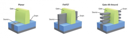
Complex Device Architectures: The evolution of semiconductor devices towards increasingly complex architectures, such as FinFETs, 3D NAND flash memory, and multi-layer interconnects, necessitates advanced etching techniques to achieve the desired device geometries and functionality. Plasma etching offers the flexibility and control required to pattern intricate device structures with multiple layers and dimensions.
Material Compatibility and Selectivity: As semiconductor materials diversify and compound semiconductor devices gain prominence, there is a growing need for plasma etching processes that can effectively etch a wide range of materials while maintaining high selectivity and uniformity. The development of specialized etching chemistries and process recipes enables precise control over material removal rates and sidewall profiles, ensuring optimal device performance and reliability.
Yield Enhancement and Process Control: Semiconductor manufacturers place a premium on yield enhancement and process control to minimize defects, improve device performance, and optimize production efficiency. Plasma etching plays a critical role in achieving these objectives by enabling precise pattern transfer with minimal variability, thereby reducing defect density, enhancing device uniformity, and maximizing wafer yields.
Emerging Applications and Technologies: The proliferation of emerging applications and technologies, such as 5G wireless communication, artificial intelligence (AI), Internet of Things (IoT), and autonomous vehicles, drives demand for semiconductor devices with specific performance characteristics and functionality. Plasma etching enables the customization and optimization of device structures to meet the requirements of these applications, opening up new market opportunities and driving innovation in semiconductor manufacturing.
Market Competition and Technological Innovation: The semiconductor industry is highly competitive, with manufacturers vying for market share, technological leadership, and innovation. Continuous advancements in plasma etching equipment, materials, and process technologies are driven by intense market competition, pushing the boundaries of etching capabilities and performance to meet evolving customer demands and gain competitive advantage.
Trends
Technological trends in semiconductor plasma etching are continuously evolving to address the growing demands of the semiconductor industry for higher performance, increased functionality, and enhanced manufacturability. Several key trends are driving innovation in plasma etching technologies:
Sub-Nanometer Feature Control: With the ongoing push towards smaller feature sizes and higher device densities, there is a critical need for plasma etching techniques capable of achieving sub-nanometer feature control. Advanced plasma sources, such as inductively coupled plasma (ICP) and electron cyclotron resonance (ECR), enable precise control over ion energy and flux, facilitating the etching of ultrafine features with sub-nanometer accuracy.
Selective Etching and Material Compatibility: As semiconductor devices incorporate a wider range of materials, including compound semiconductors, dielectrics, and metals, there is a growing demand for plasma etching processes that offer high selectivity and compatibility with diverse materials. Selective etching chemistries and process recipes enable the precise removal of target materials while minimizing damage to underlying layers and interfaces, ensuring optimal device performance and reliability.
Anisotropic Etching and Sidewall Control: Anisotropic etching, which produces vertical sidewalls with minimal sidewall roughness, is essential for fabricating advanced semiconductor structures with precise dimensions and profiles. Advanced plasma etching techniques, such as reactive ion etching (RIE) and deep reactive ion etching (DRIE), enable precise sidewall control and profile customization, facilitating the fabrication of complex device architectures, such as FinFETs, nanowires, and 3D memory structures.
Damage-Free Etching and Low-K Dielectric Preservation: With the increasing use of low-k dielectric materials in semiconductor devices to minimize signal delay and crosstalk, there is a growing emphasis on damage-free etching techniques that preserve the integrity of these sensitive materials. Plasma etching processes, such as downstream plasma etching and cryogenic etching, offer reduced ion energy and temperature, minimizing damage to low-k dielectrics and preserving their electrical properties.
Etch-Depth Uniformity and Across-Wafer Variability: Achieving uniform etch depths and minimizing across-wafer variability are critical for ensuring consistent device performance and yield in semiconductor manufacturing. Advanced plasma etching systems incorporate real-time process monitoring and control capabilities, such as optical emission spectroscopy (OES) and endpoint detection, to achieve precise etch-depth uniformity and minimize variations across the wafer, enhancing process repeatability and yield.
High-Aspect-Ratio Etching and Through-Silicon Via (TSV) Fabrication: The increasing demand for high-aspect-ratio structures, such as through-silicon vias (TSVs) and microelectromechanical systems (MEMS), requires plasma etching techniques capable of etching deep, narrow features with high aspect ratios. Deep silicon etching (DSE) and Bosch process-based etching enable the fabrication of TSVs and MEMS devices with precise control over sidewall profiles, aspect ratios, and etch depths, facilitating the integration of 3D device architectures and heterogeneous integration.
The Need for This Report
The semiconductor industry stands at the forefront of technological innovation, driving progress across various sectors from consumer electronics to healthcare and automotive. At the heart of semiconductor manufacturing lies the intricate process of plasma etching, a critical step in device fabrication that defines the intricate features and structures of modern semiconductor devices. As the demand for smaller, faster, and more energy-efficient electronic devices continues to soar, the importance of semiconductor plasma etching in enabling the production of advanced semiconductor devices cannot be overstated.
Plasma etching plays a pivotal role in the fabrication of semiconductor devices by selectively removing material layers from semiconductor substrates with unparalleled precision and control. By harnessing the unique properties of plasma—a highly ionized gas composed of charged particles—semiconductor manufacturers can achieve sub-micron feature sizes and complex device architectures essential for next-generation electronic applications. From logic and memory chips to advanced sensors and power devices, plasma etching technology underpins the development of a wide range of semiconductor products that drive innovation in virtually every aspect of modern life.
Against the backdrop of rapid technological advancements and growing market demands, the semiconductor plasma etching landscape is witnessing unprecedented evolution and innovation. Equipment manufacturers, materials suppliers, and semiconductor companies alike are continually pushing the boundaries of plasma etching technology to address the increasing complexity and performance requirements of semiconductor devices. From enhancing process uniformity and productivity to expanding the range of materials and device structures that can be etched, the semiconductor plasma etching industry is at the forefront of innovation, driving progress and shaping the future of electronics.
In this comprehensive report on semiconductor plasma etching, we delve into the intricacies of plasma etching technology, exploring its fundamental principles, key applications, and emerging trends shaping the industry. Through a detailed analysis of market dynamics, technological innovations, and competitive landscape, this report provides valuable insights and strategic intelligence for stakeholders across the semiconductor ecosystem. Whether you are a semiconductor equipment manufacturer, materials supplier, semiconductor company, or industry analyst, this report serves as a comprehensive guide to understanding the latest developments and opportunities in the dynamic field of semiconductor plasma etching.
About This Report
This 150-page report provides a comprehensive analysis of the semiconductor plasma etching market, including market size, growth drivers, challenges, and opportunities. Assessment of the competitive landscape, key players, market segmentation by product type, application, and geography.
Major segments are forecast with current and historic market shares are:
- Dielectric Etch
- Conductive Etch
- Plasma Strip
This report explores the wide range of applications of plasma etching in semiconductor manufacturing, including etching of silicon, compound semiconductors, dielectrics, metals, and other materials. Specific applications in logic devices, memory devices, sensors, power devices, and other semiconductor products.
Insights into the future outlook for semiconductor plasma etching technology, including emerging applications, market trends, and growth opportunities are detailed.
Table of Contents
Chapter 1. Introduction
- 1.1. The Need For This Report
Chapter 2. Executive Summary
- 2.1. Summary of Technical Issues
- 2.2. Summary of User Issues
- 2.3. Summary of Supplier Issues
- 2.4. Summary of Market Forecasts
Chapter 3. Technical Issues and Trends
- 3.1. Introduction
- 3.2. Processing Issues
- 3.2.1. Chlorine Versus Fluorine Processes
- 3.2.2. Multilevel Structures
- 3.2.3. New Materials
- 3.2.4. GaAs Processing
- 3.3. Plasma Stripping
- 3.3.1. Photoresist Stripping
- 3.3.2. Low-K Removal
- 3.4. Safety Issues
- 3.4.1. System Design Considerations
- 3.4.2. Gas Handling
- 3.4.3. Reactor Cleaning
Chapter 4. Market Forecast
- 4.1. Influence of Technology Trends on the Equipment Market
- 4.2. Market Forecast Assumptions
- 4.3. Market Forecast
Chapter 5. Strategic Issues: Users
- 5.1. Evaluating User Needs
- 5.1.1. Device Architecture
- 5.1.2. Wafer Starts and Throughput Requirements
- 5.1.3. Wafer Size
- 5.2. Benchmarking a Vendor
- 5.2.1. Pricing
- 5.2.2. Vendor Commitment and Attitudes
- 5.2.3. Vendor Capabilities
- 5.2.4. System Capabilities
- 5.3. Cost Analysis
- 5.3.1. Equipment Price
- 5.3.2. Installation Costs
- 5.3.3. Maintenance Costs
- 5.3.4. Sustaining Costs
- 5.3.5. Hidden Costs
- 5.4. User - Supplier Synergy
- 5.4.1. Feedback During Equipment Evaluation
- 5.4.2. Feedback During Device Production
Chapter 6. Strategic Issues: Suppliers
- 6.1. Competition
- 6.2. Customer Interaction
- 6.2.1. Customer Support
- 6.2.2. Cleanroom Needs in the Applications Lab
- 6.3. Equipment Compatibility in Class 1 Cleanrooms
- 6.3.1. Footprint Versus Serviceability
- 6.3.2. Particulate Generation
- 6.3.3. Automation
- 6.3.4. Etch Tools
- 発行日
- 発行
- Information Network
- ページ情報
- 英文
- 納期
- 2~3営業日


