Applied Materials:サービス対象市場の競合分析
Applied Materials: Competitive Analysis of Served Markets- 発行日
- ページ情報
- 英文
- 納期
- 2~3営業日
- 商品コード
- 1473282
- 翻訳ツール提供対象 PDF対応AI翻訳ツールの無料貸し出しサービスのご利用が可能です
- 電子部品/半導体関連専門 電子部品/半導体関連専門を専門とする市場調査会社です。
概要
イントロダクション
Applied Materialsは、競争の激しい半導体製造装置業界において、技術的リーダーシップ、戦略的市場ポジショニング、最新の半導体製造の課題に対する包括的アプローチにおいて傑出しています。半導体産業がノードの微細化とデバイスアーキテクチャの複雑化に向かう中、Applied Materialsのエッチング・蒸着・CMP・計測・イオン注入装置でのイノベーションは、次世代のエレクトロニクスデバイスの実現に不可欠な役割を果たすでしょう。Applied Materialsは、絶え間ないイノベーションと戦略的な先見性により、半導体技術と製造の未来を切り拓き、各市場において競合するなく主導しています。
エッチング・蒸着技術
Applied Materialsは、半導体デバイス製造の基盤となるエッチング・蒸着プロセスに優れています。同社のエッチング装置は、シリコン基板上のナノスケールの特徴を定義するのに重要なプラズマプロセスを精密に制御します。
蒸着では、化学蒸着法(CVD)、物理蒸着法(PVD)、原子層堆積法(ALD)のソリューションを提供しています。これらの技術は、半導体デバイスのさまざまな薄膜層を形成するために不可欠なもので、精度、プロセス効率、進化する業界の要件への適応性に重点を置いています。
CMP装置
CMP (化学機械研磨) 装置もApplied Materialsの注力分野で、製造工程間のウェーハ表面の平坦性を確保します。Applied MaterialsのCMP装置は製造ワークフローに統合され、スループットを最適化し、不良率を低減します。 これは製造歩留まりとコスト効率の向上に貢献し、半導体業界の目標に合致します。
計測・検査装置
計測・検査装置は、ウェーハの特性に関する重要なデータを提供し、プロセスの調整や欠陥の早期発見を促します。この種の装置は品質管理に不可欠であり、デバイスが複雑化する中、メーカーは製品の歩留まりと作業効率を高水準で維持できます。
イオン注入装置
Applied Materialsは、半導体材料のドーピングに不可欠なイオン注入技術にも特化しています。
同社のインプランターは、ドーパント種、エネルギー、ドーズ量を高精度に制御し、半導体デバイスで望ましい電気特性を実現するのに不可欠です。
当レポートについて
当レポートでは、世界の半導体製造装置市場におけるApplied Materialsの業績動向について分析し、全体的な技術開発・製造・供給動向 (2012~2023年) や、製品種類別の市場規模・シェア、主な競合企業の戦略・製品・業績、といった情報を取りまとめてお届けいたします。
目次
第1章 イントロダクション
第2章 Applied Materialsの戦略
- 市場戦略
- 製造装置の需要促進
- 国際的なプレゼンス
- 顧客ニーズを満たす
- 新CEOの戦略
- 事業戦略
- Silicon Systems Group
- Applied Global Services
- ディスプレイ
- エネルギー・環境ソリューション
- 技術戦略
- 製品戦略
- 買収戦略
- 法的戦略
- 財務分析
第3章 市場予測
- 市場促進要因
- 半導体市場
- 技術動向
- 経済動向
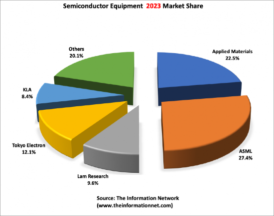
- Applied Materials:世界市場のリーダー (2019年まで)
- 市場規模と市場シェア
- 化学蒸着
- 物理蒸着
- ドライエッチング
- 急速熱処理/酸化/拡散
- シリコンエピタキシー
- CMP (化学機械平坦化)
- 計測・検査
- イオン注入
第4章 競合環境
- イントロダクション
- Lam Research
- Tokyo Electron Limited
- KLA
- ASM International
- Axcelis
- Canon Anelva
- Ebara
- Eugene Technology
- Hitachi High-Technologies
- Hitachi Kokusai Electric
- Jusung Engineering
- KC Tech
- Lasertec
- Nissin Ion Equipment
- NuFlare Technology
- Screen Semiconductor Solutions
- SEMES
- SEN
- TES
- Ulvac
- Wonik IPS
図表
List of Tables
- 3.1. Worldwide Capital Spending
- 3.2. Wafer Front End (WFE) Market By Device Type
- 3.3. Top Semiconductor Equipment Revenues
- 3.4. Worldwide CVD Market Forecast
- 3.5. Worldwide CVD Market Shares
- 3.6. Worldwide PVD Market Forecast
- 3.7. Worldwide PVD Market Shares
- 3.8. Worldwide Dry Etch Market Forecast
- 3.9. Worldwide Dry Etch Market Shares
- 3.10. Worldwide RTP/Oxidation/Diffusion Market Forecast
- 3.11. Worldwide RTP/Oxidation/Diffusion Market Shares
- 3.12. Worldwide Silicon Epitaxy Market Forecast
- 3.13. Worldwide Silicon Epitaxy Market Shares
- 3.14. Worldwide CMP Market Forecast
- 3.15. Worldwide CMP Market Shares
- 3.16. Worldwide M&I Market Forecast
- 3.17. Worldwide M&I Market Shares
- 3.18. Worldwide Ion Implantation Market Forecast
- 3.19. Worldwide Ion Implantation Market Shares
List of Figures
- 3.1. Semiconductor vs Equipment vs GDP
- 3.2. Recession Cycle
- 3.3. Semiconductor Equipment Share
- 3.4. Worldwide CVD Market Shares
- 3.5. Worldwide PVD Market Shares
- 3.6. Worldwide Dry Etch Market Shares
- 3.7. Worldwide RTP/Oxidation/Diffusion Market Shares
- 3.8. Worldwide Silicon Epitaxy Market Shares
- 3.9. Worldwide CMP Market Shares
- 3.10. Worldwide M&I Market Shares
- 3.11. Worldwide Ion Implantation Market Shares
目次
Introduction
In the competitive realm of semiconductor manufacturing equipment, Applied Materials stands out for its technological leadership, strategic market positioning, and comprehensive approach to addressing the challenges of modern semiconductor fabrication. As the industry moves towards smaller nodes and more complex device architectures, Applied Materials' innovations in etch, deposition, CMP, metrology, and ion implant equipment will continue to play a critical role in enabling the next generation of electronic devices. Through continuous innovation and strategic foresight, Applied Materials is not just competing but leading in the markets it serves, shaping the future of semiconductor technology and manufacturing.
Applied Materials' market leadership is supported by continuous innovation and a strategic approach to addressing semiconductor manufacturing challenges. The company's investment in research and development ensures its technologies meet current demands and anticipate future industry shifts.
As semiconductor fabrication evolves towards more advanced nodes and explores novel materials and architectures, Applied Materials is poised to play a central role. Its comprehensive technology portfolio, covering etch, deposition, CMP, metrology/inspection, and ion implant, positions the company as a key enabler of next-generation semiconductor devices.
Etch and Deposition Technologies
Applied Materials excels in etch and deposition processes, foundational to semiconductor device fabrication. The company's etch systems offer precise control over plasma processes, crucial for defining nanoscale features on silicon substrates. These systems enable the creation of intricate device structures required for current computing and memory applications.
In deposition, Applied Materials provides solutions across Chemical Vapor Deposition (CVD), Physical Vapor Deposition (PVD), and Atomic Layer Deposition (ALD). These technologies are critical for forming the various thin-film layers in semiconductor devices, with a focus on precision, process efficiency, and adaptability to evolving industry requirements.
CMP Systems
CMP equipment is another area of focus for Applied Materials, ensuring the planarity of wafer surfaces between fabrication steps. The company's CMP systems integrate with fabrication workflows, optimizing throughput and reducing defectivity. This contributes to improved manufacturing yields and cost efficiencies, aligning with the semiconductor industry's goals.
Metrology/Inspection Equipment
Metrology and inspection equipment from Applied Materials provides critical data on wafer properties, facilitating process adjustments and early defect identification. This category of equipment is vital for quality control, enabling manufacturers to uphold high standards of product yield and operational efficiency amid increasing device complexity.Ion Implant Equipment
Applied Materials also specializes in ion implantation technology, essential for doping semiconductor materials. The company's implanters deliver high precision in dopant species, energy, and dose control, critical for achieving desired electrical characteristics in semiconductor devices.
About This Report
This report addressed the Served Available Markets that Applied Materials competes. Namely:
- Chemical Vapor Deposition
- Physical Vapor Deposition
- Dry Etch
- Rapid Thermal Processing/Oxidation/Diffusion
- Silicon Epitaxy
- Chemical Mechanical Planarization
- Metrology and Inspection
- Ion Implantation
It presents forecasts for each sector and market shares for each equipment type between 2012 and 2023.
Table of Contents
Chapter 1. Introduction
Chapter 2. Applied's Strategies
- 2.1. Market Strategies
- 2.1.1. Driving Demand for Processing Equipment
- 2.1.2. A Global Presence
- 2.1.3. Meeting Customer Needs
- 2.1.4. New CEO's Strategy
- 2.2. Business Strategies 2.
- 2.2.1. Silicon Systems Group
- 2.2.2. Applied Global Services
- 2.2.3. Display
- 2.2.4. Energy and Environmental Solutions
- 2.3. Technology Strategies
- 2.4. Product Strategies
- 2.5. Acquisition Strategies
- 2.6. Legal Strategies
- 2.7. Financial Analysis
Chapter 3. Market Forecast
- 3.1. Market Drivers
- 3.1.1. Semiconductor Market
- 3.1.2. Technical Trends
- 3.1.3. Economic Trends
- 3.2. Applied Materials - Global Market Leader Until 2019
- 3.3. Market Size and Market Shares
- 3.3.1. Chemical Vapor Deposition
- 3.3.2. Physical Vapor Deposition
- 3.3.3. Dry Etch
- 3.3.4. Rapid Thermal Processing/Oxidation/Diffusion
- 3.3.5. Silicon Epitaxy
- 3.3.6. Chemical Mechanical Planarization
- 3.3.7. Metrology and Inspection
- 3.3.8. Ion Implantation
Chapter 4. Competitive Environment
- 4.1. Introduction
- 4.2. Lam Research
- 4.2.1. Strategies
- 4.2.2. Products
- 4.2.3. Financial Analysis
- 4.3. Tokyo Electron Limited
- 4.3.1. Strategies
- 4.3.2. Products
- 4.3.3. Financial Analysis
- 4.4. KLA
- 4.4.1. Strategies
- 4.4.2. Products
- 4.4.3. Financial Analysis
- 4.5. ASM International
- 4.5.1. Strategies
- 4.5.2. Products
- 4.5.3. Financial Analysis
- 4.6. Axcelis
- 4.6.1. Strategies
- 4.6.2. Products
- 4.6.3. Financial Analysis
- 4.7. Canon Anelva
- 4.7.1. Business Sectors Covered In The Market Analysis Chapter
- 4.7.2. Company Profile
- 4.7.3. Company Financials
- 4.8. Ebara
- 4.8.1. Business Sectors Covered In The Market Analysis Chapter
- 4.8.2. Company Profile
- 4.8.3. Company Financials
- 4.9. Eugene Technology
- 4.9.1. Business Sectors Covered In The Market Analysis Chapter
- 4.9.2. Company Profile
- 4.9.3. Company Financials
- 4.10. Hitachi High-Technologies
- 4.10.1. Business Sectors Covered In The Market Analysis Chapter
- 4.10.2. Company Profile
- 4.10.3. Company Financials
- 4.11. Hitachi Kokusai Electric
- 4.11.1. Business Sectors Covered In The Market Analysis Chapter
- 4.11.2. Company Profile
- 4.11.3. Company Financials
- 4.12. Jusung Engineering
- 4.12.1. Business Sectors Covered In The Market Analysis Chapter
- 4.12.2. Company Profile
- 4.12.3. Company Financials
- 4.13. KC Tech
- 4.13.1. Business Sectors Covered In The Market Analysis Chapter
- 4.13.2. Company Profile
- 4.13.3. Company Financials
- 4.14. Lasertec
- 4.14.1. Business Sectors Covered In The Market Analysis Chapter
- 4.14.2. Company Profile
- 4.14.3. Company Financials
- 4.15. Nissin Ion Equipment
- 4.15.1. Business Sectors Covered In The Market Analysis Chapter
- 4.15.2. Company Profile
- 4.15.3. Company Financials
- 4.16. NuFlare Technology
- 4.16.1. Business Sectors Covered In The Market Analysis Chapter
- 4.16.2. Company Profile
- 4.16.3. Company Financials
- 4.17. Screen Semiconductor Solutions
- 4.17.1. Business Sectors Covered In The Market Analysis Chapter
- 4.17.2. Company Profile
- 4.17.3. Company Financials
- 4.18. SEMES
- 4.18.1. Business Sectors Covered In The Market Analysis Chapter
- 4.18.2. Company Profile
- 4.18.3. Company Financials
- 4.19. SEN
- 4.19.1. Business Sectors Covered In The Market Analysis Chapter
- 4.19.2. Company Profile
- 4.19.3. Company Financials
- 4.20. TES
- 4.20.1. Business Sectors Covered In The Market Analysis Chapter
- 4.20.2. Company Profile
- 4.20.3. Company Financials
- 4.21. Ulvac
- 4.21.1. Business Sectors Covered In The Market Analysis Chapter
- 4.21.2. Company Profile
- 4.21.3. Company Financials
- 4.22. Wonik IPS
- 4.22.1. Business Sectors Covered In The Market Analysis Chapter
- 4.22.2. Company Profile
- 4.22.3. Company Financials
- 発行日
- 発行
- Information Network
- ページ情報
- 英文
- 納期
- 2~3営業日


