|
|
市場調査レポート
商品コード
1424146
フォトニックデザインオートメーションの市場規模と予測、世界と地域のシェア、動向、成長機会分析レポート範囲:構成別、展開別、組織規模別、用途別Photonic Design Automation Market Size and Forecasts, Global and Regional Share, Trends, and Growth Opportunity Analysis Report Coverage: By Component, Deployment, Organization Size, and Application |
||||||
|
|
|||||||
|
|||||||


| フォトニックデザインオートメーションの市場規模と予測、世界と地域のシェア、動向、成長機会分析レポート範囲:構成別、展開別、組織規模別、用途別 |
|
出版日: 2023年12月22日
発行: The Insight Partners
ページ情報: 英文 162 Pages
納期: 即納可能
|

- 全表示
- 概要
- 図表
- 目次
フォトニックデザインオートメーション市場規模は、2022年に13億9,000万米ドルと評価され、2030年には39億米ドルに達すると予測され、2022年から2030年までのCAGRは13.8%を記録すると予測されています。
エレクトロニックデザインオートメーション(EDA)ツールへのフォトニクスの統合は、フォトニックデザインオートメーション市場の重要な動向です。既存のEDAベンダーは、新興のフォトニックデザインオートメーション市場の可能性を認識し、既存のツールにフォトニクスに特化した機能や性能を組み込んでいます。この統合により、設計者はフォトニクスコンポーネントをシームレスに設計に取り入れることができ、設計プロセスを効率化し、フォトニクスデバイスの性能と機能を最適化することができます。フォトニクスをEDAツールに統合することで、設計者は使い慣れた設計環境とワークフローを活用することができ、専用のフォトニクス設計ツールに伴う学習曲線が短縮されます。また、フォトニクスをEDAツールに統合することで、エレクトロニクスとフォトニクスの融合が促進され、エレクトロニクスとフォトニクスの融合回路の開発が可能になります。この融合はシリコンフォトニクスのような技術の進歩にとって極めて重要であり、フォトニクスとIC設計の間でツール、プロセス、シミュレーションモデルを共有することで、フォトニックデザインオートメーション市場の開拓が加速されます。全体として、EDAツールへのフォトニクスの統合は、フォトニクスの重要性の高まりと、フォトニクス分野における効率的な設計プロセスと最適化技術の必要性に対する業界の認識を反映しています。これにより、設計者はフォトニクスの潜在能力を活用し、エレクトロニクス設計にシームレスに組み込むことができます。
コンパクトなモデリングおよびシミュレーションツールの進歩は、フォトニックデザインオートメーション市場に大きな影響を与えると予想されます。これらのツールは、エレクトロニクスとフォトニクスの融合において重要な役割を果たし、より迅速で効率的な設計プロセスを可能にします。コンパクトモデリングとは、複雑なフォトニクスデバイスの挙動を正確に示す簡略化された数学モデルの開発を指します。これらのモデルにより、設計者は高価で時間のかかるデバイスレベルのシミュレーションを行うことなく、フォトニックコンポーネントのシミュレーションと性能解析を行うことができます。コンパクトなモデリングを設計自動化ツールに組み込むことで、設計者は設計プロセスを合理化し、統合された電子-光回路の性能を最適化することができます。これらのツールは、電子-光協調設計から完全集積回路の開発への移行を容易にし、設計者が高性能と高効率を達成することを可能にします。このような利点により、より高度な応用が可能になり、フォトニックデザインオートメーション市場の成長が促進されます。
コンパクトなモデリングツールとシミュレーションツールをフォトニック設計自動化のワークフローに統合することで、設計者はさまざまな設計オプションを検討し、さまざまなパラメータの影響を評価し、情報に基づいた意思決定を行うことができます。これにより、設計の繰り返しが迅速化され、市場投入までの時間が短縮され、全体的な設計品質が向上します。フォトニックデザインオートメーション市場のプレーヤーが提供するコンパクトなモデリングおよびシミュレーションツールの重要性は、産業界と学界の両方によって認識されています。既存の電子設計自動化ベンダーは、自社の既存ツールにフォトニクスに特化した機能や性能を組み込んでおり、設計者はフォトニクスコンポーネントをシームレスに設計に組み込むことができます。
フォトニックデザインオートメーション市場のソリューション分野には、フォトニクス集積回路(PIC)やその他のフォトニクスデバイスの設計、シミュレーション、検証を容易にするさまざまなソフトウェアやツールが含まれます。これらのソリューションは、フォトニクス業界特有の課題やニーズに対応するために構築されています。フォトニック・デザイン・オートメーション(PDA)ツールは、シミュレーション、モデリング、解析のための高度な機能を設計者に提供することで、フォトニック・デバイスの開発と機能強化を促進するのに役立ちます。これらのツールにより、設計者は複雑なフォトニック回路の効率的な作成と検証、性能の最適化、効率的な製造プロセスの確保が可能になります。設計者がフォトニック回路を作成、レイアウトできるソフトウェアツールには、導波路、変調器、検出器、フィルタなどのコンポーネントがあります。これらのツールは、設計プロセスを合理化するために、ユーザーフレンドリーなインターフェースと高度な設計機能を提供することが多いです。フォトニックデザインオートメーション市場の成長は、通信、データセンター、ヘルスケア、センシング、イメージングなど、さまざまな用途でフォトニクスデバイスの需要が高まっていることが背景にあります。フォトニクス産業が進化と拡大を続ける中、効率的で信頼性の高い設計ツールの必要性がますます高まっています。
フォトニックデザインオートメーション市場の学術研究分野とは、フォトニクス設計や関連サービスに関連した研究開発活動を行う大学、研究機関、学術専門家の関与を指します。このセグメントは、フォトニクス分野を発展させ、設計手法、アルゴリズム、ツールの技術革新を推進する上で重要な役割を果たしています。学術機関や研究機関は、新しいコンセプトやアルゴリズム、技術を探求する研究開発活動に積極的に取り組んでいます。そのため、フォトニックデザインオートメーション市場のプレーヤーが提供するさまざまなソリューションを利用しています。これらの企業は、フォトニックコンポーネント、システム、集積回路の設計における課題や限界に対処するため、革新的なソリューションの開発に注力しています。この調査は、この分野の発展に貢献し、業界の実務者に貴重な洞察を提供します。学術研究者はしばしば、知識を共有し、アイデアを交換し、共同研究プロジェクトで協力するために、業界の専門家、他の学術機関、研究コンソーシアムと協力しています。このような共同研究は、学際的なアプローチを促進し、フォトニックデザインオートメーションにおける多様な視点の統合を可能にします。学術研究分野は、フォトニクス業界におけるコラボレーションと知識の共有を促進する上で重要な役割を果たしています。例えば、テキサス大学デザインオートメーション研究所(UTDA)は、フォトニクスデザインオートメーション市場におけるオプティクス/フォトニクス、エレクトロニクス、新興技術のデザインオートメーションアルゴリズム、手法、ツールの研究開発に注力しています。
産業研究および製造企業は、特にフォトニクス業界向けに設計自動化ツールを開発し、活用しています。これらのツールにより、設計者はレイアウト生成、シミュレーション、検証、最適化など、設計プロセスのさまざまな段階を自動化できます。これらのツールを活用することで、企業は設計サイクルを加速し、設計品質を向上させ、フォトニクス製品の市場投入までの時間を短縮することができます。産業研究・製造部門では、フォトニックデバイスの製造プロセスの最適化に注力しています。これには、高度な製造技術、プロセス制御手法、歩留まり向上戦略の開発が含まれます。製造効率や歩留まりを改善することで、企業は高品質なフォトニックコンポーネントやシステムをコスト効率よく製造することができます。フォトニックデザインオートメーション市場のプレーヤーは、しばしばフォトニックメーカーと協業し、製品の強化や販売促進を行っています。例えば、2022年3月、Cadence Design Systemsは、ハイパースケールコンピューティング、5G通信、航空宇宙システムなどのシリコンフォトニクスIC開発を加速するためにGlobalFoundriesと協業しました。このようなコラボレーションは、このような製品に関する認知度を大いに高め、フォトニックデザインオートメーション市場の成長も促進します。
世界のフォトニックデザインオートメーション市場は、コンポーネント、展開、組織規模、用途に基づいて区分されます。AIM Photonics Inc、Ansys Inc、Cadence Design Systems Inc、LioniX International BV、Luceda Photonics、Optiwave Systems Inc、Siemens AG、Synopsys Inc、SystemLab Inc、VPlphotonics GmbHなどがフォトニックデザインオートメーション市場の有力企業です。
目次
第1章 イントロダクション
第2章 エグゼクティブサマリー
- 主要洞察
- 市場の魅力
第3章 調査手法
- 調査範囲
- 2次調査
- 1次調査
第4章 フォトニックデザインオートメーション市場情勢
- PEST分析
- エコシステム分析
- バリューチェーンのベンダー一覧
第5章 フォトニックデザインオートメーション市場:主要市場力学
- フォトニックデザインオートメーション市場- 主な市場力学
- 市場促進要因
- 自動化需要の高まり
- 効率性と精度に対するニーズの高まり
- 市場抑制要因
- フォトニックデザインオートメーションの利点と能力に関する認識不足
- 市場機会
- フォトニックデバイスの進歩
- 高性能かつ環境的に持続可能なソリューションの重視
- 今後の動向
- 電子設計自動化(EDA)ツールへのフォトニクスの統合
- コンパクトなモデリングとシミュレーションツールの進歩
- 促進要因と阻害要因の影響
第6章 フォトニックデザインオートメーション市場:世界市場分析
- フォトニックデザインオートメーション市場の売上高、2022年~2030年
- フォトニックデザインオートメーション市場の予測と分析
第7章 フォトニックデザインオートメーション市場の分析:構成別
- ソリューション
- ソリューション市場、収益と2030年予測
- サービス
- サービス概要
- サービス市場、収益と2030年までの予測
第8章 フォトニックデザインオートメーション市場分析:展開別
- オンプレミス
- サービス概要
- オンプレミス市場、収益と2030年までの予測
- クラウド
- オンプレミスの概要
- クラウド市場、収益と2030年までの予測
第9章 フォトニックデザインオートメーション市場分析:組織規模別
- 中小企業
- 中小企業市場、収益と2030年までの予測
- 大企業
- 大企業の概要
- 大企業市場、収益と2030年までの予測
第10章 フォトニックデザインオートメーション市場分析:用途別
- 学術研究
- 学術研究市場、収益と2030年までの予測
- 産業研究・製造
- 産業研究・製造市場、収益と2030年までの予測
第11章 フォトニックデザインオートメーション市場:地域別分析
- 北米
- 米国
- カナダ
- 欧州
- ドイツ
- フランス
- 英国
- ロシア
- スイス
- その他欧州
- APAC
- 中国
- 日本
- 韓国
- 台湾
- APACのその他諸国
- 世界のその他の地域(RoW)
- RoW
- MEA
- 南米
- RoW
第12章 フォトニックデザインオートメーション市場:COVID-19パンデミックの影響
- COVID-19前後の影響
第13章 競合情勢
- 主要プレイヤー別ヒートマップ分析
- 企業のポジショニングと集中度
第14章 業界情勢
- 市場イニシアティブ
- 新製品開発
- 合併と買収
第15章 企業プロファイル
- Ansys Inc
- LioniX International BV
- VPlphotonics GmbH
- Optiwave Systems Inc
- Luceda Photonics
- Cadence Design Systems Inc
- Siemens AG
- Synopsys Inc
- AIM Photonics Inc
- SystemLab Inc
第16章 付録
List Of Tables
- Table 1. Photonic Design Automation Market Segmentation
- Table 2. Photonic Design Automation Market Revenue and Forecasts To 2030 (US$ Million)
- Table 3. Photonic Design Automation Market Revenue and Forecasts To 2030 (US$ Million) - Component
- Table 4. Photonic Design Automation Market Revenue and Forecasts To 2030 (US$ Million) - Deployment
- Table 5. Photonic Design Automation Market Revenue and Forecasts To 2030 (US$ Million) - Organization Size
- Table 6. Photonic Design Automation Market Revenue and Forecasts To 2030 (US$ Million) - Application
- Table 7. North America Photonic Design Automation Market Revenue and Forecasts To 2030 (US$ Mn) - By Component
- Table 8. North America Photonic Design Automation Market Revenue and Forecasts To 2030 (US$ Mn) - By Deployment
- Table 9. North America Photonic Design Automation Market Revenue and Forecasts To 2030 (US$ Mn) - By Organization Size
- Table 10. North America Photonic Design Automation Market Revenue and Forecasts To 2030 (US$ Mn) - By Application
- Table 11. North America Photonic Design Automation Market Revenue and Forecasts To 2030 (US$ Mn) - By Country
- Table 12. US Photonic Design Automation Market Revenue and Forecasts To 2030 (US$ Mn) - By Component
- Table 13. US Photonic Design Automation Market Revenue and Forecasts To 2030 (US$ Mn) - By Deployment
- Table 14. US Photonic Design Automation Market Revenue and Forecasts To 2030 (US$ Mn) - By Organization Size
- Table 15. US Photonic Design Automation Market Revenue and Forecasts To 2030 (US$ Mn) - By Application
- Table 16. Canada Photonic Design Automation Market Revenue and Forecasts To 2030 (US$ Mn) - By Component
- Table 17. Canada Photonic Design Automation Market Revenue and Forecasts To 2030 (US$ Mn) - By Deployment
- Table 18. Canada Photonic Design Automation Market Revenue and Forecasts To 2030 (US$ Mn) - By Organization Size
- Table 19. Canada Photonic Design Automation Market Revenue and Forecasts To 2030 (US$ Mn) - By Application
- Table 20. Europe Photonic Design Automation Market Revenue and Forecasts To 2030 (US$ Mn) - By Component
- Table 21. Europe Photonic Design Automation Market Revenue and Forecasts To 2030 (US$ Mn) - By Deployment
- Table 22. Europe Photonic Design Automation Market Revenue and Forecasts To 2030 (US$ Mn) - By Organization Size
- Table 23. Europe Photonic Design Automation Market Revenue and Forecasts To 2030 (US$ Mn) - By Application
- Table 24. Europe Photonic Design Automation Market Revenue and Forecasts To 2030 (US$ Mn) - By Country
- Table 25. Germany Photonic Design Automation Market Revenue and Forecasts To 2030 (US$ Mn) - By Component
- Table 26. Germany Photonic Design Automation Market Revenue and Forecasts To 2030 (US$ Mn) - By Deployment
- Table 27. Germany Photonic Design Automation Market Revenue and Forecasts To 2030 (US$ Mn) - By Organization Size
- Table 28. Germany Photonic Design Automation Market Revenue and Forecasts To 2030 (US$ Mn) - By Application
- Table 29. France Photonic Design Automation Market Revenue and Forecasts To 2030 (US$ Mn) - By Component
- Table 30. France Photonic Design Automation Market Revenue and Forecasts To 2030 (US$ Mn) - By Deployment
- Table 31. France Photonic Design Automation Market Revenue and Forecasts To 2030 (US$ Mn) - By Organization Size
- Table 32. France Photonic Design Automation Market Revenue and Forecasts To 2030 (US$ Mn) - By Application
- Table 33. UK Photonic Design Automation Market Revenue and Forecasts To 2030 (US$ Mn) - By Component
- Table 34. UK Photonic Design Automation Market Revenue and Forecasts To 2030 (US$ Mn) - By Deployment
- Table 35. UK Photonic Design Automation Market Revenue and Forecasts To 2030 (US$ Mn) - By Organization Size
- Table 36. UK Photonic Design Automation Market Revenue and Forecasts To 2030 (US$ Mn) - By Application
- Table 37. Russia Photonic Design Automation Market Revenue and Forecasts To 2030 (US$ Mn) - By Component
- Table 38. Russia Photonic Design Automation Market Revenue and Forecasts To 2030 (US$ Mn) - By Deployment
- Table 39. Russia Photonic Design Automation Market Revenue and Forecasts To 2030 (US$ Mn) - By Organization Size
- Table 40. Russia Photonic Design Automation Market Revenue and Forecasts To 2030 (US$ Mn) - By Application
- Table 41. Switzerland Photonic Design Automation Market Revenue and Forecasts To 2030 (US$ Mn) - By Component
- Table 42. Switzerland Photonic Design Automation Market Revenue and Forecasts To 2030 (US$ Mn) - By Deployment
- Table 43. Switzerland Photonic Design Automation Market Revenue and Forecasts To 2030 (US$ Mn) - By Organization Size
- Table 44. Switzerland Photonic Design Automation Market Revenue and Forecasts To 2030 (US$ Mn) - By Application
- Table 45. Rest of Europe Photonic Design Automation Market Revenue and Forecasts To 2030 (US$ Mn) - By Component
- Table 46. Rest of Europe Photonic Design Automation Market Revenue and Forecasts To 2030 (US$ Mn) - By Deployment
- Table 47. Rest of Europe Photonic Design Automation Market Revenue and Forecasts To 2030 (US$ Mn) - By Organization Size
- Table 48. Rest of Europe Photonic Design Automation Market Revenue and Forecasts To 2030 (US$ Mn) - By Application
- Table 49. APAC Photonic Design Automation Market Revenue and Forecasts To 2030 (US$ Mn) - By Component
- Table 50. APAC Photonic Design Automation Market Revenue and Forecasts To 2030 (US$ Mn) - By Deployment
- Table 51. APAC Photonic Design Automation Market Revenue and Forecasts To 2030 (US$ Mn) - By Organization Size
- Table 52. APAC Photonic Design Automation Market Revenue and Forecasts To 2030 (US$ Mn) - By Application
- Table 53. APAC Photonic Design Automation Market Revenue and Forecasts To 2030 (US$ Mn) - By Country
- Table 54. China Photonic Design Automation Market Revenue and Forecasts To 2030 (US$ Mn) - By Component
- Table 55. China Photonic Design Automation Market Revenue and Forecasts To 2030 (US$ Mn) - By Deployment
- Table 56. China Photonic Design Automation Market Revenue and Forecasts To 2030 (US$ Mn) - By Organization Size
- Table 57. China Photonic Design Automation Market Revenue and Forecasts To 2030 (US$ Mn) - By Application
- Table 58. Japan Photonic Design Automation Market Revenue and Forecasts To 2030 (US$ Mn) - By Component
- Table 59. Japan Photonic Design Automation Market Revenue and Forecasts To 2030 (US$ Mn) - By Deployment
- Table 60. Japan Photonic Design Automation Market Revenue and Forecasts To 2030 (US$ Mn) - By Organization Size
- Table 61. Japan Photonic Design Automation Market Revenue and Forecasts To 2030 (US$ Mn) - By Application
- Table 62. South Korea Photonic Design Automation Market Revenue and Forecasts To 2030 (US$ Mn) - By Component
- Table 63. South Korea Photonic Design Automation Market Revenue and Forecasts To 2030 (US$ Mn) - By Deployment
- Table 64. South Korea Photonic Design Automation Market Revenue and Forecasts To 2030 (US$ Mn) - By Organization Size
- Table 65. South Korea Photonic Design Automation Market Revenue and Forecasts To 2030 (US$ Mn) - By Application
- Table 66. Taiwan Photonic Design Automation Market Revenue and Forecasts To 2030 (US$ Mn) - By Component
- Table 67. Taiwan Photonic Design Automation Market Revenue and Forecasts To 2030 (US$ Mn) - By Deployment
- Table 68. Taiwan Photonic Design Automation Market Revenue and Forecasts To 2030 (US$ Mn) - By Organization Size
- Table 69. Taiwan Photonic Design Automation Market Revenue and Forecasts To 2030 (US$ Mn) - By Application
- Table 70. Rest of APAC Photonic Design Automation Market Revenue and Forecasts To 2030 (US$ Mn) - By Component
- Table 71. Rest of APAC Photonic Design Automation Market Revenue and Forecasts To 2030 (US$ Mn) - By Deployment
- Table 72. Rest of APAC Photonic Design Automation Market Revenue and Forecasts To 2030 (US$ Mn) - By Organization Size
- Table 73. Rest of APAC Photonic Design Automation Market Revenue and Forecasts To 2030 (US$ Mn) - By Application
- Table 74. RoW Photonic Design Automation Market Revenue and Forecasts To 2030 (US$ Mn) - By Component
- Table 75. RoW Photonic Design Automation Market Revenue and Forecasts To 2030 (US$ Mn) - By Deployment
- Table 76. RoW Photonic Design Automation Market Revenue and Forecasts To 2030 (US$ Mn) - By Organization Size
- Table 77. RoW Photonic Design Automation Market Revenue and Forecasts To 2030 (US$ Mn) - By Application
- Table 78. RoW Photonic Design Automation Market Revenue and Forecasts To 2030 (US$ Mn) - By Region
- Table 79. MEA Photonic Design Automation Market Revenue and Forecasts To 2030 (US$ Mn) - By Component
- Table 80. MEA Photonic Design Automation Market Revenue and Forecasts To 2030 (US$ Mn) - By Deployment
- Table 81. MEA Photonic Design Automation Market Revenue and Forecasts To 2030 (US$ Mn) - By Organization Size
- Table 82. MEA Photonic Design Automation Market Revenue and Forecasts To 2030 (US$ Mn) - By Application
- Table 83. SAM Photonic Design Automation Market Revenue and Forecasts To 2030 (US$ Mn) - By Component
- Table 84. SAM Photonic Design Automation Market Revenue and Forecasts To 2030 (US$ Mn) - By Deployment
- Table 85. SAM Photonic Design Automation Market Revenue and Forecasts To 2030 (US$ Mn) - By Organization Size
- Table 86. SAM Photonic Design Automation Market Revenue and Forecasts To 2030 (US$ Mn) - By Application
- Table 87. Heat Map Analysis By Key Players
- Table 88. List of Abbreviation
List Of Figures
- Figure 1. Photonic Design Automation Market Segmentation, By Geography
- Figure 2. PEST Analysis
- Figure 3. Ecosystem: Photonic Design Automation Market
- Figure 4. Impact Analysis of Drivers and Restraints
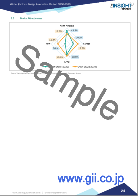
- Figure 5. Photonic Design Automation Market Breakdown by Geography, 2022 and 2030 (%)
- Figure 6. Photonic Design Automation Market Revenue (US$ Million), 2022 - 2030
- Figure 7. Photonic Design Automation Market Share (%) - Component, 2022 and 2030
- Figure 8. Solution Market Revenue and Forecasts To 2030 (US$ Million)
- Figure 9. Service Market Revenue and Forecasts To 2030 (US$ Million)
- Figure 10. Photonic Design Automation Market Share (%) - Deployment, 2022 and 2030
- Figure 11. On-Premise Market Revenue and Forecasts To 2030 (US$ Million)
- Figure 12. Cloud Market Revenue and Forecasts To 2030 (US$ Million)
- Figure 13. Photonic Design Automation Market Share (%) - Organization Size, 2022 and 2030
- Figure 14. SMEs Market Revenue and Forecasts To 2030 (US$ Million)
- Figure 15. Large Enterprises Market Revenue and Forecasts To 2030 (US$ Million)
- Figure 16. Photonic Design Automation Market Share (%) - Application, 2022 and 2030
- Figure 17. Academic Research Market Revenue and Forecasts To 2030 (US$ Million)
- Figure 18. Industrial Research & Manufacturing Market Revenue and Forecasts To 2030 (US$ Million)
- Figure 19. Photonic Design Automation Market Breakdown by Region, 2022 and 2030 (%)
- Figure 20. North America Photonic Design Automation Market Revenue and Forecasts To 2030 (US$ Mn)
- Figure 21. North America Photonic Design Automation Market Breakdown by Component (2022 and 2030)
- Figure 22. North America Photonic Design Automation Market Breakdown by Deployment (2022 and 2030)
- Figure 23. North America Photonic Design Automation Market Breakdown by Organization Size (2022 and 2030)
- Figure 24. North America Photonic Design Automation Market Breakdown by Application (2022 and 2030)
- Figure 25. North America Photonic Design Automation Market Breakdown by Key Countries, 2022 and 2030 (%)
- Figure 26. US Photonic Design Automation Market Revenue and Forecasts To 2030 (US$ Mn)
- Figure 27. Canada Photonic Design Automation Market Revenue and Forecasts To 2030 (US$ Mn)
- Figure 28. Europe Photonic Design Automation Market Revenue and Forecasts To 2030 (US$ Mn)
- Figure 29. Europe Photonic Design Automation Market Breakdown by Component (2022 and 2030)
- Figure 30. Europe Photonic Design Automation Market Breakdown by Deployment (2022 and 2030)
- Figure 31. Europe Photonic Design Automation Market Breakdown by Organization Size (2022 and 2030)
- Figure 32. Europe Photonic Design Automation Market Breakdown by Application (2022 and 2030)
- Figure 33. Europe Photonic Design Automation Market Breakdown by Key Countries, 2022 and 2030 (%)
- Figure 34. Germany Photonic Design Automation Market Revenue and Forecasts To 2030 (US$ Mn)
- Figure 35. France Photonic Design Automation Market Revenue and Forecasts To 2030 (US$ Mn)
- Figure 36. UK Photonic Design Automation Market Revenue and Forecasts To 2030 (US$ Mn)
- Figure 37. Russia Photonic Design Automation Market Revenue and Forecasts To 2030 (US$ Mn)
- Figure 38. Switzerland Photonic Design Automation Market Revenue and Forecasts To 2030 (US$ Mn)
- Figure 39. Rest of Europe Photonic Design Automation Market Revenue and Forecasts To 2030 (US$ Mn)
- Figure 40. APAC Photonic Design Automation Market Revenue and Forecasts To 2030 (US$ Mn)
- Figure 41. APAC Photonic Design Automation Market Breakdown by Component (2022 and 2030)
- Figure 42. APAC Photonic Design Automation Market Breakdown by Deployment (2022 and 2030)
- Figure 43. APAC Photonic Design Automation Market Breakdown by Organization Size (2022 and 2030)
- Figure 44. APAC Photonic Design Automation Market Breakdown by Application (2022 and 2030)
- Figure 45. APAC Photonic Design Automation Market Breakdown by Key Countries, 2022 and 2030 (%)
- Figure 46. China Photonic Design Automation Market Revenue and Forecasts To 2030 (US$ Mn)
- Figure 47. Japan Photonic Design Automation Market Revenue and Forecasts To 2030 (US$ Mn)
- Figure 48. South Korea Photonic Design Automation Market Revenue and Forecasts To 2030 (US$ Mn)
- Figure 49. Taiwan Photonic Design Automation Market Revenue and Forecasts To 2030 (US$ Mn)
- Figure 50. Rest of APAC Photonic Design Automation Market Revenue and Forecasts To 2030 (US$ Mn)
- Figure 51. RoW Photonic Design Automation Market Revenue and Forecasts To 2030 (US$ Mn)
- Figure 52. RoW Photonic Design Automation Market Breakdown by Component (2022 and 2030)
- Figure 53. RoW Photonic Design Automation Market Breakdown by Deployment (2022 and 2030)
- Figure 54. RoW Photonic Design Automation Market Breakdown by Organization Size (2022 and 2030)
- Figure 55. RoW Photonic Design Automation Market Breakdown by Application (2022 and 2030)
- Figure 56. RoW Photonic Design Automation Market Breakdown by Key Regions, 2022 and 2030 (%)
- Figure 57. MEA Photonic Design Automation Market Revenue and Forecasts To 2030 (US$ Mn)
- Figure 58. SAM Photonic Design Automation Market Revenue and Forecasts To 2030 (US$ Mn)
- Figure 59. Company Positioning & Concentration
The Photonic design automation market size was valued at US$ 1.39 billion in 2022 and is expected to reach US$ 3.90 billion by 2030; it is estimated to record a CAGR of 13.8% from 2022 to 2030.
The integration of photonics into electronic design automation (EDA) tools is a significant trend in the photonic design automation market. Established EDA vendors recognize the potential of the emerging photonic design automation market and incorporate photonics-specific features and capabilities into their existing tools. This integration enables designers to seamlessly incorporate photonics components into their designs, streamlining the design process and optimizing the performance and functionality of photonic devices. By integrating photonics into EDA tools, designers can leverage familiar design environments and workflows, reducing the learning curve associated with specialized photonic design tools. The integration of photonics into EDA tools also facilitates the convergence of electronics and photonics, enabling the development of integrated electronic-photonic circuits. This convergence is crucial for the advancement of technologies such as silicon photonics, where the sharing of tools, processes, and simulation models between photonics and IC design accelerates the development of photonic design automation market. Overall, the integration of photonics into EDA tools reflects the industry's recognition of the growing importance of photonics and the need for efficient design processes and optimization techniques in the photonic field. It enables designers to harness the potential of photonics and seamlessly incorporate it into their electronic designs.
Advancements in compact modeling and simulation tools are expected to have a significant impact on the photonic design automation market. These tools play a crucial role in the convergence of electronics and photonics, enabling faster and more efficient design processes. Compact modeling refers to the development of simplified mathematical models that precisely denote the behavior of complex photonic devices. These models allow designers to simulate and analyze the performance of photonic components without the need for expensive and time-consuming device-level simulations. By incorporating compact modeling into design automation tools, designers can streamline the design process and optimize the performance of integrated electronic-photonic circuits. These tools facilitate the transition from electronic-photonic co-design to the development of fully integrated circuits, enabling designers to achieve high performance and efficiency. Such advantages enable higher applications and promote photonic design automation market growth.
The integration of compact modeling and simulation tools into the photonic design automation workflow enables designers to explore different design options, evaluate the impact of various parameters, and make informed decisions. This leads to faster design iterations, reduced time-to-market, and improved overall design quality. The importance of compact modeling and simulation tools offered by photonic design automation market players is recognized by both industry and academia. Established electronic design automation vendors are incorporating photonics-specific features and capabilities into their existing tools, allowing designers to integrate photonics components into their designs seamlessly.
The solution segment of the photonic design automation market encompasses a variety of software and tools that facilitate the design, simulation, and verification of photonic integrated circuits (PICs) and other photonic devices. These solutions are purpose-built to address the distinctive challenges and needs of the photonics industry. Photonic design automation (PDA) tools are instrumental in expediting the development and enhancement of photonic devices by equipping designers with advanced capabilities for simulation, modeling, and analysis. These tools enable designers to effectively create and validate intricate photonic circuits, optimize performance, and ensure efficient production processes. Software tools that enable designers to create and lay out photonic circuits have components such as waveguides, modulators, detectors, and filters. These tools often provide a user-friendly interface and advanced design capabilities to streamline the design process. The photonic design automation market growth is driven by the growing demand for photonic devices in various applications, including telecommunications, data centers, healthcare, sensing, and imaging. As the photonics industry continues to evolve and expand, the need for efficient and reliable design tools becomes increasingly important.
The academic research segment of the photonic design automation market refers to the involvement of universities, research institutions, and academic professionals in conducting research and development activities related to photonic design and associated services. This segment plays a crucial role in advancing the field of photonics and driving innovation in design methodologies, algorithms, and tools. Academic institutions and research organizations actively engage in research and development activities to explore new concepts, algorithms, and techniques. They thus avail the different solutions offered by photonic design automation market players. They focus on developing innovative solutions to address the challenges and limitations in the design of photonic components, systems, and integrated circuits, by utilizing such solutions. This research contributes to the advancement of the field and provides valuable insights for industry practitioners. Academic researchers often collaborate with industry experts, other academic institutions, and research consortia to share knowledge, exchange ideas, and collaborate on joint research projects. These collaborations foster interdisciplinary approaches and enable the integration of diverse perspectives in photonic design automation. The academic research segment plays a vital role in facilitating collaboration and knowledge sharing within the photonics industry. For instance, the University of Texas Design Automation Laboratory (UTDA) focuses on the R&D of design automation algorithms, methodologies, and tools for optics/photonics, electronics, and emerging technologies in the photonic design automation market.
Industrial research and manufacturing companies develop and utilize design automation tools specifically tailored for the photonics industry. These tools enable designers to automate various stages of the design process, such as layout generation, simulation, verification, and optimization. By leveraging these tools, companies can accelerate the design cycle, improve design quality, and reduce time-to-market for photonic products. The industrial research and manufacturing segment focuses on optimizing the manufacturing processes for photonic devices. This includes developing advanced fabrication techniques, process control methodologies, and yield enhancement strategies. By improving manufacturing efficiency and yield rates, companies can achieve cost-effective production of high-quality photonic components and systems. Photonic design automation market players often collaborate with photonic manufacturers to enhance and promote their products. For instance, in March 2022, Cadence Design Systems collaborated with GlobalFoundries for accelerating silicon photonics IC development for hyperscale computing, 5G communications, and aerospace systems among others. Such collaborations greatly enhance the awareness regarding such products, and also promote photonic design automation market growth.
The global photonic design automation market is segmented based on component, deployment, organization size, and application. Based on component, the photonic design automation market is divided into solutions and services. In terms of deployment, the photonic design automation market is bifurcated into on-premise and cloud. By organization size, the photonic design automation market is bifurcated into SMEs and large enterprises. Based on application, the photonic design automation market is divided into academic research and industrial research & manufacturing. By geography, the photonic design automation market is segmented into North America, Europe, Asia Pacific (APAC), and Rest of the World (RoW). AIM Photonics Inc, Ansys Inc, Cadence Design Systems Inc, LioniX International BV, Luceda Photonics, Optiwave Systems Inc, Siemens AG, Synopsys Inc, SystemLab Inc, and VPlphotonics GmbH are among the prominent photonic design automation market players.
Reasons to Buy:
- Save and reduce time carrying out entry-level research by identifying the growth, size, leading players, and segments in the photonic design automation market.
- Highlights key business priorities in order to assist companies to realign their business strategies
- The key findings and recommendations such as specific country and segmental insight highlights crucial progressive industry trends in the photonic design automation market, thereby allowing players across the value chain to develop effective long-term strategies.
- Develop/modify business expansion plans by using substantial growth offering developed and emerging markets
- Scrutinize in-depth market trends and outlook coupled with the factors driving the market, as well as those hindering it
- Enhance the decision-making process by understanding the strategies that underpin commercial interest with respect to client products, segmentation, pricing, and distribution.
Table Of Contents
1. Introduction
- 1.1 The Insight Partners Research Report Guidance
- 1.2 Market Segmentation
2. Executive Summary
- 2.1 Key Insights
- 2.2 Market Attractiveness
3. Research Methodology
- 3.1 Coverage
- 3.2 Secondary Research
- 3.3 Primary Research
4. Photonic Design Automation Market Landscape
- 4.1 Overview
- 4.2 PEST Analysis
- 4.3 Ecosystem Analysis
- 4.3.1 List of Vendors in the Value Chain:
5. Photonic Design Automation Market - Key Market Dynamics
- 5.1 Photonic Design Automation Market - Key Market Dynamics
- 5.2 Market Drivers
- 5.2.1 Growing Demand for Automation
- 5.2.2 Increasing Need for Efficiency and Accuracy
- 5.3 Market Restraints
- 5.3.1 Lack of Awareness Regarding Benefits and Capabilities of Photonic Design Automation
- 5.4 Market Opportunities
- 5.4.1 Advancements in Photonic Devices
- 5.4.2 Emphasis on High Performance and Environmentally Sustainable Solutions
- 5.5 Future Trends
- 5.5.1 Integration of Photonics in Electronic Design Automation (EDA) Tools
- 5.5.2 Advancements in Compact Modelling and Simulation Tools
- 5.6 Impact of Drivers and Restraints:
6. Photonic Design Automation Market - Global Market Analysis
- 6.1 Photonic Design Automation Market Revenue (US$ Million), 2022 - 2030
- 6.2 Photonic Design Automation Market Forecast and Analysis
7. Photonic Design Automation Market Analysis - Component
- 7.1 Solution
- 7.1.1 Overview
- 7.1.2 Solution Market, Revenue and Forecast to 2030 (US$ Million)
- 7.2 Service
- 7.2.1 Overview
- 7.2.2 Service Market, Revenue and Forecast to 2030 (US$ Million)
8. Photonic Design Automation Market Analysis - Deployment
- 8.1 On-Premise
- 8.1.1 Overview
- 8.1.2 On-Premise Market, Revenue and Forecast to 2030 (US$ Million)
- 8.2 Cloud
- 8.2.1 Overview
- 8.2.2 Cloud Market, Revenue and Forecast to 2030 (US$ Million)
9. Photonic Design Automation Market Analysis - Organization Size
- 9.1 SMEs
- 9.1.1 Overview
- 9.1.2 SMEs Market, Revenue and Forecast to 2030 (US$ Million)
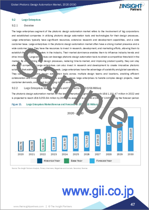
- 9.2 Large Enterprises
- 9.2.1 Overview
- 9.2.2 Large Enterprises Market, Revenue and Forecast to 2030 (US$ Million)
10. Photonic Design Automation Market Analysis - Application
- 10.1 Academic Research
- 10.1.1 Overview
- 10.1.2 Academic Research Market, Revenue and Forecast to 2030 (US$ Million)
- 10.2 Industrial Research & Manufacturing
- 10.2.1 Overview
- 10.2.2 Industrial Research & Manufacturing Market, Revenue and Forecast to 2030 (US$ Million)
11. Photonic Design Automation Market - Geographical Analysis
- 11.1 Overview
- 11.2 North America
- 11.2.1 North America Photonic Design Automation Market Overview
- 11.2.2 North America Photonic Design Automation Market Revenue and Forecasts to 2030 (US$ Mn)
- 11.2.3 North America Photonic Design Automation Market Breakdown by Component
- 11.2.3.1 North America Photonic Design Automation Market Revenue and Forecasts and Analysis - By Component
- 11.2.4 North America Photonic Design Automation Market Breakdown by Deployment
- 11.2.4.1 North America Photonic Design Automation Market Revenue and Forecasts and Analysis - By Deployment
- 11.2.5 North America Photonic Design Automation Market Breakdown by Organization Size
- 11.2.5.1 North America Photonic Design Automation Market Revenue and Forecasts and Analysis - By Organization Size
- 11.2.6 North America Photonic Design Automation Market Breakdown by Application
- 11.2.6.1 North America Photonic Design Automation Market Revenue and Forecasts and Analysis - By Application
- 11.2.7 North America Photonic Design Automation Market Revenue and Forecasts and Analysis - By Country
- 11.2.7.1 North America Photonic Design Automation Market Revenue and Forecasts and Analysis - By Country
- 11.2.7.2 US Photonic Design Automation Market Revenue and Forecasts to 2030 (US$ Mn)
- 11.2.7.2.1 US Photonic Design Automation Market Breakdown, by Component
- 11.2.7.2.2 US Photonic Design Automation Market Breakdown, by Deployment
- 11.2.7.2.3 US Photonic Design Automation Market Breakdown, by Organization Size
- 11.2.7.2.4 US Photonic Design Automation Market Breakdown, by Application
- 11.2.7.3 Canada Photonic Design Automation Market Revenue and Forecasts to 2030 (US$ Mn)
- 11.2.7.3.1 Canada Photonic Design Automation Market Breakdown, by Component
- 11.2.7.3.2 Canada Photonic Design Automation Market Breakdown, by Deployment
- 11.2.7.3.3 Canada Photonic Design Automation Market Breakdown, by Organization Size
- 11.2.7.3.4 Canada Photonic Design Automation Market Breakdown, by Application
- 11.3 Europe
- 11.3.1 Europe Photonic Design Automation Market Overview
- 11.3.2 Europe Photonic Design Automation Market Revenue and Forecasts to 2030 (US$ Mn)
- 11.3.3 Europe Photonic Design Automation Market Breakdown by Component
- 11.3.3.1 Europe Photonic Design Automation Market Revenue and Forecasts and Analysis - By Component
- 11.3.4 Europe Photonic Design Automation Market Breakdown by Deployment
- 11.3.4.1 Europe Photonic Design Automation Market Revenue and Forecasts and Analysis - By Deployment
- 11.3.5 Europe Photonic Design Automation Market Breakdown by Organization Size
- 11.3.5.1 Europe Photonic Design Automation Market Revenue and Forecasts and Analysis - By Organization Size
- 11.3.6 Europe Photonic Design Automation Market Breakdown by Application
- 11.3.6.1 Europe Photonic Design Automation Market Revenue and Forecasts and Analysis - By Application
- 11.3.7 Europe Photonic Design Automation Market Revenue and Forecasts and Analysis - By Country
- 11.3.7.1 Europe Photonic Design Automation Market Revenue and Forecasts and Analysis - By Country
- 11.3.7.2 Germany Photonic Design Automation Market Revenue and Forecasts to 2030 (US$ Mn)
- 11.3.7.2.1 Germany Photonic Design Automation Market Breakdown, by Component
- 11.3.7.2.2 Germany Photonic Design Automation Market Breakdown, by Deployment
- 11.3.7.2.3 Germany Photonic Design Automation Market Breakdown, by Organization Size
- 11.3.7.2.4 Germany Photonic Design Automation Market Breakdown, by Application
- 11.3.7.3 France Photonic Design Automation Market Revenue and Forecasts to 2030 (US$ Mn)
- 11.3.7.3.1 France Photonic Design Automation Market Breakdown, by Component
- 11.3.7.3.2 France Photonic Design Automation Market Breakdown, by Deployment
- 11.3.7.3.3 France Photonic Design Automation Market Breakdown, by Organization Size
- 11.3.7.3.4 France Photonic Design Automation Market Breakdown, by Application
- 11.3.7.4 UK Photonic Design Automation Market Revenue and Forecasts to 2030 (US$ Mn)
- 11.3.7.4.1 UK Photonic Design Automation Market Breakdown, by Component
- 11.3.7.4.2 UK Photonic Design Automation Market Breakdown, by Deployment
- 11.3.7.4.3 UK Photonic Design Automation Market Breakdown, by Organization Size
- 11.3.7.4.4 UK Photonic Design Automation Market Breakdown, by Application
- 11.3.7.5 Russia Photonic Design Automation Market Revenue and Forecasts to 2030 (US$ Mn)
- 11.3.7.5.1 Russia Photonic Design Automation Market Breakdown, by Component
- 11.3.7.5.2 Russia Photonic Design Automation Market Breakdown, by Deployment
- 11.3.7.5.3 Russia Photonic Design Automation Market Breakdown, by Organization Size
- 11.3.7.5.4 Russia Photonic Design Automation Market Breakdown, by Application
- 11.3.7.6 Switzerland Photonic Design Automation Market Revenue and Forecasts to 2030 (US$ Mn)
- 11.3.7.6.1 Switzerland Photonic Design Automation Market Breakdown, by Component
- 11.3.7.6.2 Switzerland Photonic Design Automation Market Breakdown, by Deployment
- 11.3.7.6.3 Switzerland Photonic Design Automation Market Breakdown, by Organization Size
- 11.3.7.6.4 Switzerland Photonic Design Automation Market Breakdown, by Application
- 11.3.7.7 Rest of Europe Photonic Design Automation Market Revenue and Forecasts to 2030 (US$ Mn)
- 11.3.7.7.1 Rest of Europe Photonic Design Automation Market Breakdown, by Component
- 11.3.7.7.2 Rest of Europe Photonic Design Automation Market Breakdown, by Deployment
- 11.3.7.7.3 Rest of Europe Photonic Design Automation Market Breakdown, by Organization Size
- 11.3.7.7.4 Rest of Europe Photonic Design Automation Market Breakdown, by Application
- 11.4 APAC
- 11.4.1 APAC Photonic Design Automation Market Overview
- 11.4.2 APAC Photonic Design Automation Market Revenue and Forecasts to 2030 (US$ Mn)
- 11.4.3 APAC Photonic Design Automation Market Breakdown by Component
- 11.4.3.1 APAC Photonic Design Automation Market Revenue and Forecasts and Analysis - By Component
- 11.4.4 APAC Photonic Design Automation Market Breakdown by Deployment
- 11.4.4.1 APAC Photonic Design Automation Market Revenue and Forecasts and Analysis - By Deployment
- 11.4.5 APAC Photonic Design Automation Market Breakdown by Organization Size
- 11.4.5.1 APAC Photonic Design Automation Market Revenue and Forecasts and Analysis - By Organization Size
- 11.4.6 APAC Photonic Design Automation Market Breakdown by Application
- 11.4.6.1 APAC Photonic Design Automation Market Revenue and Forecasts and Analysis - By Application
- 11.4.7 APAC Photonic Design Automation Market Revenue and Forecasts and Analysis - By Country
- 11.4.7.1 APAC Photonic Design Automation Market Revenue and Forecasts and Analysis - By Country
- 11.4.7.2 China Photonic Design Automation Market Revenue and Forecasts to 2030 (US$ Mn)
- 11.4.7.2.1 China Photonic Design Automation Market Breakdown, by Component
- 11.4.7.2.2 China Photonic Design Automation Market Breakdown, by Deployment
- 11.4.7.2.3 China Photonic Design Automation Market Breakdown, by Organization Size
- 11.4.7.2.4 China Photonic Design Automation Market Breakdown, by Application
- 11.4.7.3 Japan Photonic Design Automation Market Revenue and Forecasts to 2030 (US$ Mn)
- 11.4.7.3.1 Japan Photonic Design Automation Market Breakdown, by Component
- 11.4.7.3.2 Japan Photonic Design Automation Market Breakdown, by Deployment
- 11.4.7.3.3 Japan Photonic Design Automation Market Breakdown, by Organization Size
- 11.4.7.3.4 Japan Photonic Design Automation Market Breakdown, by Application
- 11.4.7.4 South Korea Photonic Design Automation Market Revenue and Forecasts to 2030 (US$ Mn)
- 11.4.7.4.1 South Korea Photonic Design Automation Market Breakdown, by Component
- 11.4.7.4.2 South Korea Photonic Design Automation Market Breakdown, by Deployment
- 11.4.7.4.3 South Korea Photonic Design Automation Market Breakdown, by Organization Size
- 11.4.7.4.4 South Korea Photonic Design Automation Market Breakdown, by Application
- 11.4.7.5 Taiwan Photonic Design Automation Market Revenue and Forecasts to 2030 (US$ Mn)
- 11.4.7.5.1 Taiwan Photonic Design Automation Market Breakdown, by Component
- 11.4.7.5.2 Taiwan Photonic Design Automation Market Breakdown, by Deployment
- 11.4.7.5.3 Taiwan Photonic Design Automation Market Breakdown, by Organization Size
- 11.4.7.5.4 Taiwan Photonic Design Automation Market Breakdown, by Application
- 11.4.7.6 Rest of APAC Photonic Design Automation Market Revenue and Forecasts to 2030 (US$ Mn)
- 11.4.7.6.1 Rest of APAC Photonic Design Automation Market Breakdown, by Component
- 11.4.7.6.2 Rest of APAC Photonic Design Automation Market Breakdown, by Deployment
- 11.4.7.6.3 Rest of APAC Photonic Design Automation Market Breakdown, by Organization Size
- 11.4.7.6.4 Rest of APAC Photonic Design Automation Market Breakdown, by Application
- 11.5 Rest of the World (RoW)
- 11.5.1 RoW Photonic Design Automation Market Overview
- 11.5.2 RoW Photonic Design Automation Market Revenue and Forecasts to 2030 (US$ Mn)
- 11.5.3 RoW Photonic Design Automation Market Breakdown by Component
- 11.5.3.1 RoW Photonic Design Automation Market Revenue and Forecasts and Analysis - By Component
- 11.5.4 RoW Photonic Design Automation Market Breakdown by Deployment
- 11.5.4.1 RoW Photonic Design Automation Market Revenue and Forecasts and Analysis - By Deployment
- 11.5.5 RoW Photonic Design Automation Market Breakdown by Organization Size
- 11.5.5.1 RoW Photonic Design Automation Market Revenue and Forecasts and Analysis - By Organization Size
- 11.5.6 RoW Photonic Design Automation Market Breakdown by Application
- 11.5.6.1 RoW Photonic Design Automation Market Revenue and Forecasts and Analysis - By Application
- 11.5.7 RoW Photonic Design Automation Market Revenue and Forecasts and Analysis - By Region
- 11.5.7.1 RoW Photonic Design Automation Market Revenue and Forecasts and Analysis - By Region
- 11.5.7.2 MEA Photonic Design Automation Market Revenue and Forecasts to 2030 (US$ Mn)
- 11.5.7.2.1 MEA Photonic Design Automation Market Breakdown, by Component
- 11.5.7.2.2 MEA Photonic Design Automation Market Breakdown, by Deployment
- 11.5.7.2.3 MEA Photonic Design Automation Market Breakdown, by Organization Size
- 11.5.7.2.4 MEA Photonic Design Automation Market Breakdown, by Application
- 11.5.7.3 SAM Photonic Design Automation Market Revenue and Forecasts to 2030 (US$ Mn)
- 11.5.7.3.1 SAM Photonic Design Automation Market Breakdown, by Component
- 11.5.7.3.2 SAM Photonic Design Automation Market Breakdown, by Deployment
- 11.5.7.3.3 SAM Photonic Design Automation Market Breakdown, by Organization Size
- 11.5.7.3.4 SAM Photonic Design Automation Market Breakdown, by Application
12. Photonic Design Automation Market - Impact of COVID-19 Pandemic
- 12.1 Pre & Post Covid-19 Impact
13. Competitive Landscape
- 13.1 Heat Map Analysis By Key Players
- 13.2 Company Positioning & Concentration
14. Industry Landscape
- 14.1 Overview
- 14.2 Market Initiative
- 14.2 New Product Development
- 14.3 Merger and Acquisition
15. Company Profiles
- 15.1 Ansys Inc
- 15.1.1 Key Facts
- 15.1.2 Business Description
- 15.1.3 Products and Services
- 15.1.4 Financial Overview
- 15.1.5 SWOT Analysis
- 15.1.6 Key Developments
- 15.2 LioniX International BV
- 15.2.1 Key Facts
- 15.2.2 Business Description
- 15.2.3 Products and Services
- 15.2.4 Financial Overview
- 15.2.5 SWOT Analysis
- 15.2.6 Key Developments
- 15.3 VPlphotonics GmbH
- 15.3.1 Key Facts
- 15.3.2 Business Description
- 15.3.3 Products and Services
- 15.3.4 Financial Overview
- 15.3.5 SWOT Analysis
- 15.3.6 Key Developments
- 15.4 Optiwave Systems Inc
- 15.4.1 Key Facts
- 15.4.2 Business Description
- 15.4.3 Products and Services
- 15.4.4 Financial Overview
- 15.4.5 SWOT Analysis
- 15.4.6 Key Developments
- 15.5 Luceda Photonics
- 15.5.1 Key Facts
- 15.5.2 Business Description
- 15.5.3 Products and Services
- 15.5.4 Financial Overview
- 15.5.5 SWOT Analysis
- 15.5.6 Key Developments
- 15.6 Cadence Design Systems Inc
- 15.6.1 Key Facts
- 15.6.2 Business Description
- 15.6.3 Products and Services
- 15.6.4 Financial Overview
- 15.6.5 SWOT Analysis
- 15.6.6 Key Developments
- 15.7 Siemens AG
- 15.7.1 Key Facts
- 15.7.2 Business Description
- 15.7.3 Products and Services
- 15.7.4 Financial Overview
- 15.7.5 SWOT Analysis
- 15.7.6 Key Developments
- 15.8 Synopsys Inc
- 15.8.1 Key Facts
- 15.8.2 Business Description
- 15.8.3 Products and Services
- 15.8.4 Financial Overview
- 15.8.5 SWOT Analysis
- 15.8.6 Key Developments
- 15.9 AIM Photonics Inc
- 15.9.1 Key Facts
- 15.9.2 Business Description
- 15.9.3 Products and Services
- 15.9.4 Financial Overview
- 15.9.5 SWOT Analysis
- 15.9.6 Key Developments
- 15.10 SystemLab Inc
- 15.10.1 Key Facts
- 15.10.2 Business Description
- 15.10.3 Products and Services
- 15.10.4 Financial Overview
- 15.10.5 SWOT Analysis
- 15.10.6 Key Developments
16. Appendix
- 16.1 Word Index