|
|
市場調査レポート
商品コード
1494914
半導体製造材料市場の2030年までの予測:材料タイプ、半導体タイプ、エンドユーザー、地域別の世界分析Semiconductor Fabrication Material Market Forecasts to 2030 - Global Analysis By Material Type (Chemical Mechanical Polishing Slurry & Pads, Photomasks, Photoresist Ancillaries and Other Material Types), Semiconductor Type, End User and By Geography |
||||||
|
|||||||
カスタマイズ可能
|
|||||||

| 半導体製造材料市場の2030年までの予測:材料タイプ、半導体タイプ、エンドユーザー、地域別の世界分析 |
|
出版日: 2024年06月06日
発行: Stratistics Market Research Consulting
ページ情報: 英文 200+ Pages
納期: 2~3営業日
|

全表示
- 概要
- 図表
- 目次
Stratistics MRCによると、世界の半導体製造材料市場は2024年に689億米ドルを占め、予測期間中にCAGR 7.2%で成長し、2030年には1,046億米ドルに達する見込みです。
半導体製造材料は、集積回路などの半導体デバイスの製造工程で使用される必須物質です。これらの材料には、シリコンウエハー、フォトマスク、化学機械研磨(CMP)スラリーやパッド、ウェットケミカル、工業用ガス、フォトレジストなどが含まれます。これらの材料は、半導体ウエハーのパターニングに重要な役割を果たし、さまざまなデバイスを駆動する電子部品の製造を可能にしています。
米国商務省(DOC)によると、半導体サプライチェーンの世界半導体市場規模は、2020年の4,400億米ドルから2021年には5,530億米ドルとなり、25%以上の成長を示しています。
民生用電子機器の需要増加
半導体製造材料市場は、民生用電子機器に対する需要の増加によって大きく牽引されています。世界中の消費者がスマートフォンからスマートホームデバイスに至るまで最新のガジェットを求め続けているため、高度な半導体製造材料の必要性が高まっています。これらの材料は、これらの機器に電力を供給する集積回路やチップの製造に不可欠であるため、市場の成長に拍車をかけています。
原材料価格の変動
原材料価格の変動は、半導体製造用材料市場の大きな抑制要因となっています。半導体製造に使用されるシリコン、金属、化学物質のコストは、市場の需要、地政学的緊張、サプライチェーンの混乱によって大きく変動する可能性があります。こうした変動は半導体製造の全体コストに影響を与え、メーカーの収益性と価格戦略に影響を与えます。
新興技術の採用拡大
5G、人工知能、モノのインターネットなどの新興技術の採用拡大が、半導体製造材料市場に大きな機会をもたらしています。これらの技術には、より高い性能と効率を持つ高度な半導体デバイスが必要とされ、これらの厳しい要件を満たすことができる革新的な製造材料への需要を牽引しています。
技術の陳腐化
技術の陳腐化は半導体製造用材料市場にとって脅威です。技術の急速な進歩は、既存の材料や製造プロセスを時代遅れにする可能性があり、企業は継続的な革新と適応を余儀なくされます。このような絶え間ない進化の必要性は研究開発資源を疲弊させ、市場力学に影響を与える可能性があります。
COVID-19の影響:
COVID-19の大流行は、半導体製造材料市場にさまざまな影響を与えました。当初、サプライチェーンと製造業務の混乱が短期的な需要減退につながった。しかし、パンデミックはデジタルトランスフォーメーションを加速させ、コンシューマーエレクトロニクスとコネクティビティソリューションの需要を増加させ、最終的には市場の回復と成長を刺激しました。
予測期間中、シリコンウエハーセグメントが最大となる見込み
予測期間中、シリコンウエハー部門が最大となる見込みです。シリコン・ウエハーは半導体製造の基盤材料であり、ほとんどの集積回路の基板となります。シリコン・ウエハーの需要は、電子機器の世界の需要に直結しており、市場の重要なセグメントとなっています。
予測期間中のCAGRはPタイプが最も高いと予想される
P-Typeセグメントは予測期間中に最も高いCAGRが見込まれます。P型半導体材料は、豊富な正孔を形成するためにドーピングされており、様々な電子部品の機能にとって極めて重要です。半導体デバイスの複雑化と、より効率的なエネルギー伝導の必要性が、P型材料の需要を牽引しています。
最大のシェアを占める地域:
アジア太平洋地域は、いくつかの要因から最大のシェアを誇り、半導体製造材料市場を独占することになります。これには、中国、韓国、台湾のような国々に主要な半導体製造拠点が存在し、先端製造技術への多額の投資が需要を牽引していることが含まれます。さらに、有利な政府政策、熟練労働力、強固なサプライチェーン・ネットワークが、半導体製造材料の生産と消費のリーダーとしてのこの地域の地位をさらに強化しています。
CAGRが最も高い地域:
アジア太平洋地域も半導体製造用材料市場の急成長が予想され、CAGRは最も高いです。この地域の成長の原動力となっているのは、民生用電子機器需要の増加、新興技術の採用拡大、工業化の進展です。政府の支援策と急成長する半導体産業のエコシステムが、この地域の成長予測に寄与しています。さらに、5G、IoT、AIなどの先端技術の急速な採用が、アジア太平洋地域における半導体製造材料の需要をさらに促進しています。
無料のカスタマイズ提供:
本レポートをご購読のお客様には、以下の無料カスタマイズオプションのいずれかをご利用いただけます:
- 企業プロファイル
- 追加市場プレイヤーの包括的プロファイリング(3社まで)
- 主要企業のSWOT分析(3社まで)
- 地域セグメンテーション
- 顧客の関心に応じた主要国の市場推計・予測・CAGR(注:フィージビリティチェックによる)
- 競合ベンチマーキング
- 製品ポートフォリオ、地理的プレゼンス、戦略的提携に基づく主要企業のベンチマーキング
目次
第1章 エグゼクティブサマリー
第2章 序文
- 概要
- ステークホルダー
- 調査範囲
- 調査手法
- データマイニング
- データ分析
- データ検証
- 調査アプローチ
- 調査情報源
- 1次調査情報源
- 2次調査情報源
- 前提条件
第3章 市場動向分析
- 促進要因
- 抑制要因
- 機会
- 脅威
- エンドユーザー分析
- 新興市場
- COVID-19の影響
第4章 ポーターのファイブフォース分析
- 供給企業の交渉力
- 買い手の交渉力
- 代替品の脅威
- 新規参入業者の脅威
- 競争企業間の敵対関係
第5章 世界の半導体製造材料市場:材料タイプ別
- 化学機械研磨(CMP)スラリーとパッド
- 産業ガス
- 三フッ化窒素(NF3)
- フッ化タングステン(WF6)
- 洗浄ガス(CIF3,20%F2N)
- バルクガスモノシラン
- フォトマスク
- フォトレジスト関連製品
- フォトレジスト
- シリコンウエハー
- スパッタターゲット
- 湿式化学薬品
- 静電チャック
- その他の材料タイプ
第6章 世界の半導体製造材料市場:半導体タイプ別
- N型
- P型
第7章 世界の半導体製造材料市場:エンドユーザー別
- 建築
- 自動車
- 通信
- コンピューター
- 消費財
- 防衛・航空宇宙
- 電気・電子
- プリント基板(PCB)アセンブリ
- 半導体パッケージングおよびアセンブリ
- パワーエレクトロニクスのパッケージング・組み立て
- 産業
- 医療とヘルスケア
- 発電
- 輸送機関
- 製造業
- エネルギー
- 石油ガス
- 太陽光エネルギー
- 風力エネルギー
- その他のエンドユーザー
第8章 世界の半導体製造材料市場:地域別
- 北米
- 米国
- カナダ
- メキシコ
- 欧州
- ドイツ
- 英国
- イタリア
- フランス
- スペイン
- その他欧州
- アジア太平洋地域
- 日本
- 中国
- インド
- オーストラリア
- ニュージーランド
- 韓国
- その他アジア太平洋地域
- 南米
- アルゼンチン
- ブラジル
- チリ
- その他南米
- 中東・アフリカ
- サウジアラビア
- アラブ首長国連邦
- カタール
- 南アフリカ
- その他中東とアフリカ
第9章 主な発展
- 契約、パートナーシップ、コラボレーション、合弁事業
- 買収と合併
- 新製品発売
- 事業拡大
- その他の主要戦略
第10章 企業プロファイリング
- Applied Materials, Inc.
- Lam Research Corporation
- Tokyo Electron Limited
- ASML Holding N.V.
- KLA Corporation
- SCREEN Semiconductor Solutions Co., Ltd.
- Hitachi High-Technologies Corporation
- JSR Corporation
- Sumitomo Chemical Co., Ltd.
- Shin-Etsu Chemical Co., Ltd.
- Entegris, Inc.
- ASM International N.V.
- Advantest Corporation
- Tokuyama Corporation
- Dow Electronic Materials
- Cabot Microelectronics Corporation
- Tokai Carbon Co., Ltd.
- Merck KGaA
- Birla Carbon
List of Tables
Table 1 Global Semiconductor Fabrication Material Market Outlook, By Region (2022-2030) ($MN)
- Table 2 Global Semiconductor Fabrication Material Market Outlook, By Material Type (2022-2030) ($MN)
- Table 3 Global Semiconductor Fabrication Material Market Outlook, By Chemical Mechanical Polishing (CMP) Slurry & Pads (2022-2030) ($MN)
- Table 4 Global Semiconductor Fabrication Material Market Outlook, By Industrial Gases (2022-2030) ($MN)
- Table 5 Global Semiconductor Fabrication Material Market Outlook, By Nitrogen Trifluoride (NF3) (2022-2030) ($MN)
- Table 6 Global Semiconductor Fabrication Material Market Outlook, By Tungsten Fluoride (WF6) (2022-2030) ($MN)
- Table 7 Global Semiconductor Fabrication Material Market Outlook, By Cleaning Gas (CIF3,20%F2N) (2022-2030) ($MN)
- Table 8 Global Semiconductor Fabrication Material Market Outlook, By Bulk Gas Monosilane (2022-2030) ($MN)
- Table 9 Global Semiconductor Fabrication Material Market Outlook, By Photomasks (2022-2030) ($MN)
- Table 10 Global Semiconductor Fabrication Material Market Outlook, By Photoresist Ancillaries (2022-2030) ($MN)
- Table 11 Global Semiconductor Fabrication Material Market Outlook, By Photoresists (2022-2030) ($MN)
- Table 12 Global Semiconductor Fabrication Material Market Outlook, By Silicon Wafers (2022-2030) ($MN)
- Table 13 Global Semiconductor Fabrication Material Market Outlook, By Sputter Targets (2022-2030) ($MN)
- Table 14 Global Semiconductor Fabrication Material Market Outlook, By Wet Chemicals (2022-2030) ($MN)
- Table 15 Global Semiconductor Fabrication Material Market Outlook, By Electrostatic Chucks (2022-2030) ($MN)
- Table 16 Global Semiconductor Fabrication Material Market Outlook, By Other Material Types (2022-2030) ($MN)
- Table 17 Global Semiconductor Fabrication Material Market Outlook, By Semiconductor Type (2022-2030) ($MN)
- Table 18 Global Semiconductor Fabrication Material Market Outlook, By N-Type (2022-2030) ($MN)
- Table 19 Global Semiconductor Fabrication Material Market Outlook, By P-Type (2022-2030) ($MN)
- Table 20 Global Semiconductor Fabrication Material Market Outlook, By End User (2022-2030) ($MN)
- Table 21 Global Semiconductor Fabrication Material Market Outlook, By Architecture (2022-2030) ($MN)
- Table 22 Global Semiconductor Fabrication Material Market Outlook, By Automotive (2022-2030) ($MN)
- Table 23 Global Semiconductor Fabrication Material Market Outlook, By Telecommunication (2022-2030) ($MN)
- Table 24 Global Semiconductor Fabrication Material Market Outlook, By Computers (2022-2030) ($MN)
- Table 25 Global Semiconductor Fabrication Material Market Outlook, By Consumer Goods (2022-2030) ($MN)
- Table 26 Global Semiconductor Fabrication Material Market Outlook, By Defense & Aerospace (2022-2030) ($MN)
- Table 27 Global Semiconductor Fabrication Material Market Outlook, By Electrical and Electronics (2022-2030) ($MN)
- Table 28 Global Semiconductor Fabrication Material Market Outlook, By Printed Circuit Board (PCB) Assembly (2022-2030) ($MN)
- Table 29 Global Semiconductor Fabrication Material Market Outlook, By Semiconductor Packaging and Assembly (2022-2030) ($MN)
- Table 30 Global Semiconductor Fabrication Material Market Outlook, By Power Electronics Packaging and Assembly (2022-2030) ($MN)
- Table 31 Global Semiconductor Fabrication Material Market Outlook, By Industrial (2022-2030) ($MN)
- Table 32 Global Semiconductor Fabrication Material Market Outlook, By Medical and Healthcare (2022-2030) ($MN)
- Table 33 Global Semiconductor Fabrication Material Market Outlook, By Power Generation (2022-2030) ($MN)
- Table 34 Global Semiconductor Fabrication Material Market Outlook, By Transportation (2022-2030) ($MN)
- Table 35 Global Semiconductor Fabrication Material Market Outlook, By Manufacturing (2022-2030) ($MN)
- Table 36 Global Semiconductor Fabrication Material Market Outlook, By Energy (2022-2030) ($MN)
- Table 37 Global Semiconductor Fabrication Material Market Outlook, By Oil & Gas (2022-2030) ($MN)
- Table 38 Global Semiconductor Fabrication Material Market Outlook, By Solar Energy (2022-2030) ($MN)
- Table 39 Global Semiconductor Fabrication Material Market Outlook, By Wind Energy (2022-2030) ($MN)
- Table 40 Global Semiconductor Fabrication Material Market Outlook, By Other End Users (2022-2030) ($MN)
Note: Tables for North America, Europe, APAC, South America, and Middle East & Africa Regions are also represented in the same manner as above.
According to Stratistics MRC, the Global Semiconductor Fabrication Material Market is accounted for $68.9 billion in 2024 and is expected to reach $104.6 billion by 2030 growing at a CAGR of 7.2% during the forecast period. Semiconductor fabrication materials are essential substances used in the process of manufacturing semiconductor devices, such as integrated circuits. These materials include silicon wafers, photomasks, chemical mechanical polishing (CMP) slurry and pads, wet chemicals, industrial gases, and photoresists. They play a critical role in patterning semiconductor wafers, enabling the creation of electronic components that power a wide range of devices.
According to the U.S. Department of Commerce (DOC), the semiconductor supply chain highlights that the global semiconductor market was valued at $553 billion in 2021, up from $440 billion in 2020, representing a growth of over 25%.
Market Dynamics:
Driver:
Increasing demand for consumer electronics
The semiconductor fabrication material market is significantly driven by the increasing demand for consumer electronics. As consumers worldwide continue to seek the latest gadgets, from smartphones to smart home devices, the need for advanced semiconductor fabrication materials escalates. These materials are crucial for manufacturing the integrated circuits and chips that power these devices, thus fueling market growth.
Restraint:
Fluctuations in raw material prices
Fluctuations in the prices of raw materials pose a major restraint to the semiconductor fabrication material market. The cost of silicon, metals, and chemicals used in semiconductor manufacturing can vary widely due to market demand, geopolitical tensions, and supply chain disruptions. These fluctuations impact the overall cost of semiconductor production, affecting profitability and pricing strategies for manufacturers.
Opportunity:
Growing adoption of emerging technologies
The growing adoption of emerging technologies such as 5G, artificial intelligence, and the internet of things present a significant opportunity for the semiconductor fabrication material market. These technologies require advanced semiconductor devices with higher performance and efficiency, driving the demand for innovative fabrication materials that can meet these stringent requirements.
Threat:
Technological obsolescence
Technological obsolescence represents a threat to the semiconductor fabrication material market. Rapid advancements in technology can render existing materials and manufacturing processes outdated, forcing companies to continuously innovate and adapt. This constant need for evolution can strain research and development resources and impact the market dynamics.
Covid-19 Impact:
The Covid-19 pandemic had a mixed impact on the semiconductor fabrication material market. Initially, disruptions in supply chains and manufacturing operations led to a short-term decline in demand. However, the pandemic also accelerated digital transformation and increased demand for consumer electronics and connectivity solutions, ultimately stimulating recovery and growth in the market.
The silicon wafers segment is expected to be the largest during the forecast period
The silicon wafers segment is expected to be the largest during the forecast period. Silicon wafers are the foundational material for semiconductor manufacturing, serving as the substrate for most integrated circuits. The demand for silicon wafers is directly tied to the global demand for electronic devices, making it a critical segment in the market.
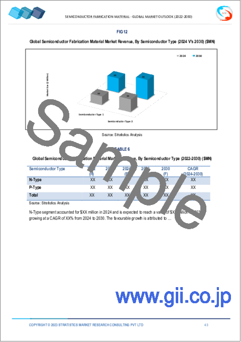
The P-Type segment is expected to have the highest CAGR during the forecast period
The P-Type segment is expected to have the highest CAGR during the forecast period. P-Type semiconductor materials are doped to create an abundance of holes, making them crucial for the function of various electronic components. The growing complexity of semiconductor devices and the need for more efficient energy conduction are driving the demand for P-Type materials.
Region with largest share:
The Asia Pacific region is set to dominate the semiconductor fabrication material market, boasting the largest share due to several factors. These include the presence of major semiconductor manufacturing hubs in countries like China, South Korea, and Taiwan, where significant investments in advanced fabrication technologies are driving demand. Additionally, favorable government policies, a skilled workforce, and robust supply chain networks further bolster the region's position as a leader in semiconductor fabrication material production and consumption.
Region with highest CAGR:
The Asia Pacific region also anticipates rapid growth in the semiconductor fabrication material market, with the highest CAGR. The region's growth is fueled by increasing demand for consumer electronics, expanding adoption of emerging technologies, and ongoing industrialization. Supportive government initiatives and a burgeoning semiconductor industry ecosystem contribute to the region's projected growth. Additionally, the rapid adoption of advanced technologies like 5G, IoT, and AI further fuels the demand for semiconductor fabrication materials in the Asia Pacific region.
Key players in the market
Some of the key players in Semiconductor Fabrication Material Market include Applied Materials, Inc., Lam Research Corporation, Tokyo Electron Limited, ASML Holding N.V., KLA Corporation, SCREEN Semiconductor Solutions Co., Ltd., Hitachi High-Technologies Corporation, JSR Corporation, Sumitomo Chemical Co., Ltd., Shin-Etsu Chemical Co., Ltd., Entegris, Inc., ASM International N.V., Advantest Corporation, Tokuyama Corporation, Dow Electronic Materials, Cabot Microelectronics Corporation, Tokai Carbon Co., Ltd., Merck KGaA and Birla Carbon.
Key Developments:
In June 2023, Semiconductor technology is critical in enabling a global digital economy. With device complexity on the rise, advanced technology scaling is harder than ever. It means finding new ways to accelerate innovation, at lower cost, across a globally distributed industry, all while reducing the industry's environmental impact. To overcome these challenges, a new paradigm must be embraced: A physical and virtual connected semiconductor ecosystem that will enable labs and fabs to unleash the power of innovation for a better world
In May 2023, Applied Materials, a maker of semiconductor fabrication equipment, plans to plow $4 billion into a collaborative research and development facility in Silicon Valley over the next seven years. The 180,000 square foot Equipment and Process Innovation and Commercialization (EPIC) Center is expected to create 2,000 engineering jobs and provide chipmakers and university researchers with a space to develop and prototype designs on next-generation process tech and pre-release equipment, if the facility comes online in 2026.
In February 2023, Applied Materials, Inc. unveiled a breakthrough in patterning technology that allows chipmakers to create high-performance transistors and interconnect wiring with fewer EUV lithography steps, thereby lowering the cost, complexity and environmental impact of advanced chipmaking.
Material Types Covered:
- Chemical Mechanical Polishing (CMP) Slurry & Pads
- Industrial Gases
- Photomasks
- Photoresist Ancillaries
- Photoresists
- Silicon Wafers
- Sputter Targets
- Wet Chemicals
- Electrostatic Chucks
- Other Material Types
Semiconductor Types Covered:
- N-Type
- P-Type
End Users Covered:
- Architecture
- Automotive
- Telecommunication
- Computers
- Consumer Goods
- Defense & Aerospace
- Electrical and Electronics
- Industrial
- Medical and Healthcare
- Power Generation
- Transportation
- Manufacturing
- Other End Users
Regions Covered:
- North America
- US
- Canada
- Mexico
- Europe
- Germany
- UK
- Italy
- France
- Spain
- Rest of Europe
- Asia Pacific
- Japan
- China
- India
- Australia
- New Zealand
- South Korea
- Rest of Asia Pacific
- South America
- Argentina
- Brazil
- Chile
- Rest of South America
- Middle East & Africa
- Saudi Arabia
- UAE
- Qatar
- South Africa
- Rest of Middle East & Africa
What our report offers:
- Market share assessments for the regional and country-level segments
- Strategic recommendations for the new entrants
- Covers Market data for the years 2022, 2023, 2024, 2026, and 2030
- Market Trends (Drivers, Constraints, Opportunities, Threats, Challenges, Investment Opportunities, and recommendations)
- Strategic recommendations in key business segments based on the market estimations
- Competitive landscaping mapping the key common trends
- Company profiling with detailed strategies, financials, and recent developments
- Supply chain trends mapping the latest technological advancements
Free Customization Offerings:
All the customers of this report will be entitled to receive one of the following free customization options:
- Company Profiling
- Comprehensive profiling of additional market players (up to 3)
- SWOT Analysis of key players (up to 3)
- Regional Segmentation
- Market estimations, Forecasts and CAGR of any prominent country as per the client's interest (Note: Depends on feasibility check)
- Competitive Benchmarking
- Benchmarking of key players based on product portfolio, geographical presence, and strategic alliances
Table of Contents
1 Executive Summary
2 Preface
- 2.1 Abstract
- 2.2 Stake Holders
- 2.3 Research Scope
- 2.4 Research Methodology
- 2.4.1 Data Mining
- 2.4.2 Data Analysis
- 2.4.3 Data Validation
- 2.4.4 Research Approach
- 2.5 Research Sources
- 2.5.1 Primary Research Sources
- 2.5.2 Secondary Research Sources
- 2.5.3 Assumptions
3 Market Trend Analysis
- 3.1 Introduction
- 3.2 Drivers
- 3.3 Restraints
- 3.4 Opportunities
- 3.5 Threats
- 3.6 End User Analysis
- 3.7 Emerging Markets
- 3.8 Impact of Covid-19
4 Porters Five Force Analysis
- 4.1 Bargaining power of suppliers
- 4.2 Bargaining power of buyers
- 4.3 Threat of substitutes
- 4.4 Threat of new entrants
- 4.5 Competitive rivalry
5 Global Semiconductor Fabrication Material Market, By Material Type
- 5.1 Introduction
- 5.2 Chemical Mechanical Polishing (CMP) Slurry & Pads
- 5.3 Industrial Gases
- 5.3.1 Nitrogen Trifluoride (NF3)
- 5.3.2 Tungsten Fluoride (WF6)
- 5.3.3 Cleaning Gas (CIF3,20%F2N)
- 5.3.4 Bulk Gas Monosilane
- 5.4 Photomasks
- 5.5 Photoresist Ancillaries
- 5.6 Photoresists
- 5.7 Silicon Wafers
- 5.8 Sputter Targets
- 5.9 Wet Chemicals
- 5.10 Electrostatic Chucks
- 5.11 Other Material Types
6 Global Semiconductor Fabrication Material Market, By Semiconductor Type
- 6.1 Introduction
- 6.2 N-Type
- 6.3 P-Type
7 Global Semiconductor Fabrication Material Market, By End User
- 7.1 Introduction
- 7.2 Architecture
- 7.3 Automotive
- 7.4 Telecommunication
- 7.5 Computers
- 7.6 Consumer Goods
- 7.7 Defense & Aerospace
- 7.8 Electrical and Electronics
- 7.8.1 Printed Circuit Board (PCB) Assembly
- 7.8.2 Semiconductor Packaging and Assembly
- 7.8.3 Power Electronics Packaging and Assembly
- 7.9 Industrial
- 7.10 Medical and Healthcare
- 7.11 Power Generation
- 7.12 Transportation
- 7.13 Manufacturing
- 7.14 Energy
- 7.14.1 Oil & Gas
- 7.14.2 Solar Energy
- 7.14.3 Wind Energy
- 7.15 Other End Users
8 Global Semiconductor Fabrication Material Market, By Geography
- 8.1 Introduction
- 8.2 North America
- 8.2.1 US
- 8.2.2 Canada
- 8.2.3 Mexico
- 8.3 Europe
- 8.3.1 Germany
- 8.3.2 UK
- 8.3.3 Italy
- 8.3.4 France
- 8.3.5 Spain
- 8.3.6 Rest of Europe
- 8.4 Asia Pacific
- 8.4.1 Japan
- 8.4.2 China
- 8.4.3 India
- 8.4.4 Australia
- 8.4.5 New Zealand
- 8.4.6 South Korea
- 8.4.7 Rest of Asia Pacific
- 8.5 South America
- 8.5.1 Argentina
- 8.5.2 Brazil
- 8.5.3 Chile
- 8.5.4 Rest of South America
- 8.6 Middle East & Africa
- 8.6.1 Saudi Arabia
- 8.6.2 UAE
- 8.6.3 Qatar
- 8.6.4 South Africa
- 8.6.5 Rest of Middle East & Africa
9 Key Developments
- 9.1 Agreements, Partnerships, Collaborations and Joint Ventures
- 9.2 Acquisitions & Mergers
- 9.3 New Product Launch
- 9.4 Expansions
- 9.5 Other Key Strategies
10 Company Profiling
- 10.1 Applied Materials, Inc.
- 10.2 Lam Research Corporation
- 10.3 Tokyo Electron Limited
- 10.4 ASML Holding N.V.
- 10.5 KLA Corporation
- 10.6 SCREEN Semiconductor Solutions Co., Ltd.
- 10.7 Hitachi High-Technologies Corporation
- 10.8 JSR Corporation
- 10.9 Sumitomo Chemical Co., Ltd.
- 10.10 Shin-Etsu Chemical Co., Ltd.
- 10.11 Entegris, Inc.
- 10.12 ASM International N.V.
- 10.13 Advantest Corporation
- 10.14 Tokuyama Corporation
- 10.15 Dow Electronic Materials
- 10.16 Cabot Microelectronics Corporation
- 10.17 Tokai Carbon Co., Ltd.
- 10.18 Merck KGaA
- 10.19 Birla Carbon
