|
|
市場調査レポート
商品コード
1138042
プラズマエッチング装置市場- 成長、動向、予測(2022年-2027年)Plasma Etching Equipment Market - Growth, Trends, and Forecasts (2022 - 2027) |
||||||
|
|
|||||||
|
● お客様のご希望に応じて、既存データの加工や未掲載情報(例:国別セグメント)の追加などの対応が可能です。 詳細はお問い合わせください。 |
|||||||

| プラズマエッチング装置市場- 成長、動向、予測(2022年-2027年) |
|
出版日: 2022年10月13日
発行: Mordor Intelligence
ページ情報: 英文 120 Pages
納期: 2~3営業日
|
- 全表示
- 概要
- 目次
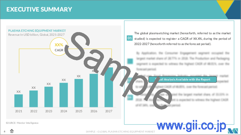
プラズマエッチング装置市場は、予測期間中にCAGR7.8%を記録すると予想されています。
プラズマエッチング装置の需要は、予測期間中、エッチングプロセスの使用により、さらに小さな寸法を実現するエッチング技術および関連装置の重要性が高まっていることが要因であると考えられます。プラズマエッチングは、マイクロエレクトロニクス産業における微細化のための厳しいプロセス要求に対応するための様々な修正を可能にしています。
主なハイライト
- プラズマエッチングは洗練された汎用性の高い技術であり、様々なデバイスを作成することができます。現在、半導体メーカーは、薬品の消費量が少なく、自動化やウエハー製造に適していることから、従来のウェットエッチングからプラズマエッチングシステムに切り替えつつあります。小型でエネルギー効率に優れ、高性能な電子機器への要求が高まる中、半導体集積回路(IC)の小型化のニーズが高まっています。ICを小型化するためには、微細な形状を持つ高度な回路形成工程を経る必要があり、正確なパターン転写が求められます。
- プラズマエッチングは、半導体やマイクロエレクトロメカニカルシステム産業で広く使用されています。例えば、プリント基板(PCB)の製造では、機械加工後や電気メッキ前の回路をプラズマ洗浄するために等方性エッチングが使用されます。また、ウエハーに回路パターンを形成する際には、異方性エッチングが用いられます。この異方性プラズマエッチングは高エネルギーであり、反応性イオンエッチング(RIE)と呼ばれます。
- さらに、世界中のさまざまな消費者に技術的に高度なインテリジェントデバイスを提供するためにIoTアプリケーションで行われている大規模な技術的アップグレードも、高度な半導体の需要を加速させ、市場の成長にプラスの影響を与えると予測されています。IoTアプリケーションの成長に伴い、スマートデバイスが増加し、半導体の小型化が進んでいるため、プラズマエッチングの需要が高まっています。
- スマートフォンなど半導体ICを必要とするアプリケーションも、無線技術(5G)や人工知能などの技術進歩がこれらの分野の動向に大きな影響を与えており、家電や自動車などの業界におけるプラズマエッチングの需要全体を押し上げる要因となっています。また、モノのインターネット(IoT)機器の増加により、半導体業界はインテリジェントな製品を実現するためにこの装置への投資を余儀なくされると予想されます。SEMI Silicon Manufacturers Group(SMG)は、シリコンウェーハ業界の四半期レビューで、2021年第3四半期の世界のシリコンウェーハ出荷量が3.3%増の36億4900万平方インチとなり、業界最高を更新したことを明らかにしました。2021年第3四半期のシリコンウェーハの出荷量は、前年同期比16.4%増の31億3500万平方インチとなっています。
- しかし、この装置はウェットケミカルエッチング装置よりもコストが高いことが多いです。また、ウェットケミカルエッチングによるレジストの消費が早いため、本装置が提供する選択性はウェットケミカルエッチング装置と比較して低くなります。これらは、市場の成長を阻む主な要因の一部です。
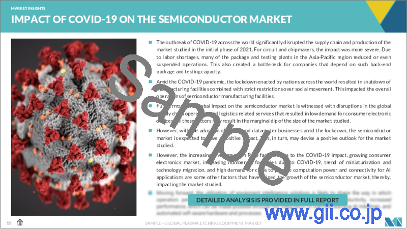
- COVID-19の大流行により、半導体製造装置業界では、世界のほとんどの地域でロックダウンが続き、いくつかのアイテムの製造が停止しました。このような状況下、半導体製造装置業界では、世界の需給逼迫の影響を受け、家電製品の需要が減少しました。また、自動車の世界の需要減退と輸出の減少が半導体市場に悪影響を及ぼし、半導体製造装置の需要に減速が見られるようになりました。しかし、産業活動が大流行前の水準に戻るにつれて、需要は徐々に牽引されると予想されます。
主な市場動向
コンシューマーエレクトロニクス分野が需要を牽引
- 電気・電子産業には、航空宇宙製品、発光ダイオードなどのランプ・照明器具、テレビ、家電製品、電子医療機器、マイクロエレクトロニクス部品、自動車用ソフトウェアなどの家電製品、車載診断装置(OBD)、車載用タッチパネル、カメラ、ナビゲーションシステムなどの電気・電子部品など、さまざまな製品が含まれています。半導体産業の成長を牽引するもうひとつの重要な要因は、民生用電子機器分野の拡大です。
- COVID-19の大流行により、世界中の人々が仕事や学習、余暇を自宅で過ごすことを余儀なくされ、家電製品の需要が高まっています。しかし、世界のチップ不足とサプライチェーンのボトルネックにより、多くの電気機器はまだ供給不足の状態にあります。前年と比較すると、2020年の世界の電気・電子部門は成長しなかっています。2021年には成長が予測され、2022年にはCOVID-19に関連する懸念事項への対応が進み、産業は成長すると予想されています。ドイツの電気・デジタル分野の協会であるZVEIによると、2021年から2022年にかけて、この産業は世界的に6%成長すると予測されました。
- インドなどの新興国は、2013年以降、データ通信料が95%削減され、その結果、スマートフォンユーザーが驚異的に増加しています。ASSOCHAMによると、インドのスマートフォンユーザーは2017年の4億6800万人から2022年にはCAGR12.9%で約8億5900万人に倍増すると予想されています。このようなスマートフォン普及の大幅な数量増加は、スマートフォン産業における半導体の需要を生み出すと予想されます。さらに、Indian Brand Equity Foundationによると、インドでは家電・民生機器産業が倍増し、2025年には211億8000万米ドルに達すると予想されています。
- 世界各国の政府が、自国の需要の一部を満たすために投資を増やし、支援的な規制を設けていることが、研究対象市場の成長にとって良い市場シナリオを生み出しています。
- さらに、家電業界からの需要の高まりも、半導体メーカーによる生産設備の拡張を後押ししています。例えば、2021年10月、台湾積体電路製造公司(TSMC)は、現地の顧客のニーズに対応するため、日本に新しい準専門工場を建設する計画を発表しました。この工場は、2024年後半の稼働時には、日本で最も先進的なロジック工場となる予定です。このような拡張は、調査された市場の成長機会を創出することになります。
アジア太平洋地域が大きな成長を遂げる見込み
- アジア太平洋地域は、プラズマエッチング装置の主要市場の1つです。その主な理由は、大手半導体メーカーの存在、多数のエンドユーザー産業における先端技術に対する需要の高まり、家電産業の高い成長、同地域の半導体産業に対する政府の支援政策などです。
- また、スマートデバイスやポータブルデバイスの需要の高まりは、小型集積回路(IC)の需要を押し上げ、予測期間中にプラズマエッチング装置市場のニーズを急速に高めると予想されています。GSMAによると、中国のユニークモバイル加入者率は世界最高水準にあります。2020年には12億2000万人であったが、2026年には12億6000万人に達し、全人口の約85%を占めると推定されます。
- この地域の多くの国の政府は、半導体産業を支援しています。例えば、中国では、半導体産業の現地化を支援する政策が継続的に導入されています。Made in China 2025」イニシアティブは、半導体装置生産の現地化のための明確なロードマップを提供しています。SEMIによると、ここ数年、厦門のUMC、南京のTSMC、合肥のPSC、成都のGLOBALFOUNDRIES、武漢と南京のYMTCなど、中国で多くの新しい12インチファブプロジェクトが発表、建設開始、あるいは立ち上げ段階にあるとのことです。
- 同様に、政府が複数のPLIスキームを発表した後、複数の半導体製造企業がインドに製造施設を設立するために投資を増やしています。例えば、2022年8月、タミル・ナードゥ州に拠点を置く半導体チップメーカーのポリマテックは、製造施設を拡張するために10億米ドル相当の投資を発表しました。
競合情勢について
プラズマエッチング装置市場は競合が多いです。既存のプレーヤーが市場に浸透しているため、ベンダー間の競争は激しく、今後も成長が見込まれます。主なプレイヤーは、アプライドマテリアルズ、ラムリサーチ、東京エレクトロンなど。
- 2022年3月- エッチング、蒸着、表面処理加工装置メーカーのサムコは、新しいプラズマエッチングクラスターツール"Cluster H"を発表しました。Cluster Hは、最先端のプラズマ技術を駆使し、SiC/GaNパワーデバイス、高周波フィルター、GaAs VCSEL、CMOSイメージセンサー、マイクロOLED/LED、先進パッケージングなどの化合物半導体デバイスを本格的に生産することができます。
- 2022年3月- ドライエッチング装置メーカーのAPTCは、2023年のデモテキストに提供する300mm酸化膜エッチング装置を開発中と発表しました。APTCは、まずプラズマ源を用いてポリシリコンをエッチングするエッチング装置を提供しました。これにより、同社はドライエッチング装置市場におけるプレゼンスをさらに拡大することに注力します。
その他の特典。
- エクセル形式の市場予測(ME)シート
- アナリストによる3ヶ月間のサポート
目次
第1章 イントロダクション
- 調査の前提条件と市場の定義
- 調査対象範囲
第2章 調査手法
第3章 エグゼクティブサマリー
第4章 マーケットインサイト
- 市場概要
- 産業バリューチェーン分析
- 産業の魅力-ポーターのファイブフォース分析
- 新規参入業者の脅威
- 買い手の交渉力
- 供給企業の交渉力
- 代替品の脅威
- 競争企業間の敵対関係
- COVID-19が市場に与える影響
第5章 市場の力学
- 市場促進要因
- 半導体産業の成長
- 小型でエネルギー効率に優れた電子機器への需要の高まり
- 市場抑制要因
- 回路構造の微細化に伴う複雑化
第6章 市場セグメンテーション
- タイプ別
- リアクティブイオンエッチング(RIE)
- 誘導結合プラズマエッチング(ICP)
- 深堀り反応性イオンエッチング(DRIE)
- その他のタイプ
- アプリケーション別
- 産業用途
- 医療用
- 民生用エレクトロニクス
- その他の用途
- 地域別
- 北米
- 欧州
- アジア太平洋地域
- 世界のその他の地域
第7章 競合情勢
- 企業プロファイル
- SPTS Technologies(KLA company)
- Applied Materials Inc.
- Lam Research Corporation
- Oxford Instruments PLC
- Tokyo Electron Limited
- Plasma Etch Inc.
- Plasma-Therm LLC
- Thierry Corporation
- Samco Inc.
- Advanced Micro-Fabrication Equipment Inc.
- Sentech Instruments GmbH
- GigaLane Co. Ltd
第8章 投資分析
第9章 市場の将来展望
The Plasma Etching Equipment Market is expected to register a CAGR of 7.8% over the forecast period. The demand for plasma etching equipment is expected to be driven by the increasing importance of etching technology and related equipment with the use of etching processes to achieve even smaller dimensions over the forecast period. Plasma etching has enabled various modifications to address stringent process demands for miniaturization in the microelectronics industry.
Key Highlights
- Plasma etching is a sophisticated, versatile technology that creates a wide range of devices. Today, semiconductor manufacturers are switching to the plasma etch system from traditional wet etching, as it consumes fewer chemicals and is more suitable for automation and single wafer manufacturing. Increasing demand for compact, energy-efficient electronic devices having improved performance is boosting the need for developing miniature semiconductor integrated circuits (ICs). For miniaturizing IC, the course has to undergo an advanced circuit fabrication process with small geometries and thus requires precise pattern transfer.
- Plasma etching is used extensively in the semiconductor and microelectromechanical systems industries. For instance, in manufacturing printed circuit boards (PCBs), isotropic etching is used to plasma clean circuits after machining and before electroplating. Anisotropic etching is used to form circuit patterns in wafers. This anisotropic plasma etching is highly energetic and called reactive ion etching (RIE).
- Moreover, massive technological upgradation taking place in the IoT application to offer technologically advanced intelligent devices to different consumers across the globe is also predicted to accelerate the demand for advanced semiconductors, thereby positively affecting the market's growth. With the growth in IoT applications, smart devices are increasing, giving rise to miniature semiconductors, thus raising the demand for plasma etching.
- Smartphones and other applications that require semiconductor ICs are other factors driving the overall demand for plasma etching in consumer electronics, automotive, and other industries, as technology advancements like wireless technologies (5G) and artificial intelligence have significantly impacted the trend of these sectors. Also, the increasing number of Internet of Things (IoT) devices is expected to force the semiconductor industry to invest in this equipment to attain intelligent products. The SEMI Silicon Manufacturers Group (SMG) revealed in its quarterly review of the silicon wafer industry that worldwide silicon wafer shipments grew 3.3% to 3,649 million square inches in the third quarter of 2021, which was a new industry high. Shipments of silicon wafers in the third quarter of 2021 increased by 16.4% over the same quarter the previous year, to 3,135 million square inches.
- However, this equipment is often costlier than wet-chemical etching equipment. Also, due to faster consumption of resists due to wet chemical etching, the selectivity offered by this equipment is reduced compared to wet-chemical etching equipment. These are some of the primary factors challenging the growth of the market.
- The COVID-19 pandemic halted the manufacturing of several items in the semiconductor production equipment industry, owing to continued lockdown in most regions across the world. Lockdown measures reduced demand for consumer electronic gadgets, which had a global impact on the semiconductor sector. The continued decline in worldwide demand and export shipments for automobiles provided a negative impact on the semiconductor market, which is currently slowing the demand for semiconductor manufacturing equipment. However, the demand is expected to gain traction gradually with the industrial activities returning back to the pre-pandemic level.
Key Market Trends
Consumer Electronics Segment to Drive the Demand
- The electrical and electronics industry includes a wide range of products, including aerospace products, lamps and light fixtures, including light-emitting diodes, consumer electronics, such as television sets, electrical household appliances, electronic medical equipment, microelectronic components, and automotive software, and electrical and electronic components, like on-board diagnostics (OBD), in-car touch screens, cameras, and navigation systems. Another key factor driving the semiconductor industry's growth is the expanding consumer electronics sector.
- People worldwide were forced to work, learn, and spend their free time at home due to the COVID-19 pandemic, which increased the demand for consumer electronics. Many electrical devices, however, are still in low supply due to a global lack of chips and supply chain bottlenecks. Compared to the previous year, the global electrical and electronics sector did not grow in 2020. The industry was predicted to grow in 2021 and is expected to grow in 2022, as the concerns linked to COVID-19 are being increasingly addressed. According to ZVEI, a German association of the electrical and digital sector, the industry was predicted to grow by 6% globally between 2021 and 2022.
- Emerging economies, such as India, have witnessed a reduction in data costs by 95% since 2013, resulting in tremendous growth in smartphone users. According to ASSOCHAM, smartphone users in India were expected to double from 468 million users in 2017 to approximately 859 million by 2022, at a CAGR of 12.9%. Such significant volume growth in smartphone adoption is expected to create a demand for semiconductors in the smartphone industry. Moreover, the appliances and consumer electronics industry is expected to double, to reach USD 21.18 billion by 2025, in India, according to the Indian Brand Equity Foundation.
- Increasing investment and supportive regulations being framed by governments worldwide to meet some portion of their local demand are creating a good market scenario for the studied market growth.
- Furthermore, the growing demand from the consumer electronics industry is also encouraging semiconductor manufacturers to expand their production facilities. For instance, in October 2021, Taiwan Semiconductor Manufacturing Company Ltd (TSMC) announced its plans to build a new semi-specialist factory in Japan to meet the needs of local customers. The factory will be the most advanced logic factory in Japan when it operates in the second half of 2024. Such expansions will create opportunities for the studied market to grow.
Asia-Pacific is Expected to Witness Significant Growth
- Asia-Pacific is one of the prominent markets for plasma etching equipment, primarily attributed to the presence of some of the leading semiconductor manufacturers, growing demand for advanced technologies across numerous end-user industries, high consumer electronics industry growth, and supporting government policies for the semiconductor industry in the region.
- Growing demand for smart and portable devices is also anticipated to boost the demand for miniature integrated circuits (ICs), which is expected to rapidly fuel the need for the plasma etching equipment market over the forecast period. According to GSMA, China's unique mobile subscriber rate is among the highest in the world. While it was 1.22 billion in 2020, it is estimated to reach 1.26 billion in 2026, approximately 85% of the total population.
- The governments in many countries across the region are supporting the semiconductor industry. For instance, China has continuously introduced policies to support the localization of the semiconductor industry. The "Made in China 2025" initiative has provided a clear roadmap for the localization of semiconductor equipment production. According to SEMI, in recent years, many new 12-inch fab projects have been announced, started construction, or are in the ramp-up stage in China, including UMC in Xiamen, TSMC in Nanjing, PSC in Hefei, GLOBALFOUNDRIES in Chengdu, as well as YMTC in Wuhan and Nanjing.
- Similarly, several semiconductor manufacturing companies are increasing their investment to establish manufacturing facilities in India after the government announced several PLI schemes. For instance, in August 2022, Polymatech, a Tamil Nadu based semiconductor chip manufacturer, announced an investment worth USD 1 billion to expand its manufacturing facilities.
Competitive Landscape
The plasma etching equipment market is competitive. There is enormous competition among the vendors owing to the intense market penetration of some existing players in the market expected to grow further. Some major players include Applied Materials Inc., Lam Research Corporation, and Tokyo Electron Ltd., among others.
- March 2022 - Samco, an etching, deposition, and surface treatment processing equipment manufacturer, introduced the new plasma etching cluster tool "Cluster H." By leveraging its cutting-edge plasma technology, Cluster H provides the full-scale production capabilities for compound semiconductor devices such as SiC/GaN power devices, high-frequency filters, GaAs VCSELs, CMOS image sensors, micro-OLED/LED, and advanced packaging.
- March 2022 - APTC, a dry etching equipment maker, announced that it is developing a 300mm oxide etching equipment to offer for a demo text in 2023. APTC offered etching equipment that uses a plasma source to etch polysilicon first. With this, the company focuses on further expanding its presence in the dry etching equipment market.
Additional Benefits:
- The market estimate (ME) sheet in Excel format
- 3 months of analyst support
TABLE OF CONTENTS
1 INTRODUCTION
- 1.1 Study Assumptions and Market Definition
- 1.2 Scope of the Study
2 RESEARCH METHODOLOGY
3 EXECUTIVE SUMMARY
4 MARKET INSIGHTS
- 4.1 Market Overview
- 4.2 Industry Value Chain Analysis
- 4.3 Industry Attractiveness - Porter's Five Forces Analysis
- 4.3.1 Threat of New Entrants
- 4.3.2 Bargaining Power of Buyers
- 4.3.3 Bargaining Power of Suppliers
- 4.3.4 Threat of Substitute Products
- 4.3.5 Intensity of Competitive Rivalry
- 4.4 Impact of COVID-19 on the Market
5 MARKET DYNAMICS
- 5.1 Market Drivers
- 5.1.1 Growth of the Semiconductor Industry
- 5.1.2 Rising Demand for Compact and Energy Efficient Electronic Devices
- 5.2 Market Restraints
- 5.2.1 Growing Complexities Related to Miniaturized Structures of Circuits
6 MARKET SEGMENTATION
- 6.1 By Type
- 6.1.1 Reactive Ion Etching (RIE)
- 6.1.2 Inductively Coupled Plasma Etching (ICP)
- 6.1.3 Deep Reactive Ion Etching (DRIE)
- 6.1.4 Other Types
- 6.2 By Application
- 6.2.1 Industrial Applications
- 6.2.2 Medical Applications
- 6.2.3 Consumer Electronics
- 6.2.4 Other Applications
- 6.3 Geography
- 6.3.1 North America
- 6.3.2 Europe
- 6.3.3 Asia Pacific
- 6.3.4 Rest of the World
7 COMPETITIVE LANDSCAPE
- 7.1 Company Profiles
- 7.1.1 SPTS Technologies (KLA company)
- 7.1.2 Applied Materials Inc.
- 7.1.3 Lam Research Corporation
- 7.1.4 Oxford Instruments PLC
- 7.1.5 Tokyo Electron Limited
- 7.1.6 Plasma Etch Inc.
- 7.1.7 Plasma-Therm LLC
- 7.1.8 Thierry Corporation
- 7.1.9 Samco Inc.
- 7.1.10 Advanced Micro-Fabrication Equipment Inc.
- 7.1.11 Sentech Instruments GmbH
- 7.1.12 GigaLane Co. Ltd