
|
市場調査レポート
商品コード
1642058
ガリウムヒ素(GaAs)ウエハ:市場シェア分析、産業動向、成長予測(2025~2030年)Gallium Arsenide GaAs Wafer - Market Share Analysis, Industry Trends & Statistics, Growth Forecasts (2025 - 2030) |
||||||
カスタマイズ可能
適宜更新あり
|
|||||||
| ガリウムヒ素(GaAs)ウエハ:市場シェア分析、産業動向、成長予測(2025~2030年) |
|
出版日: 2025年01月05日
発行: Mordor Intelligence
ページ情報: 英文 120 Pages
納期: 2~3営業日
|

全表示
- 概要
- 目次
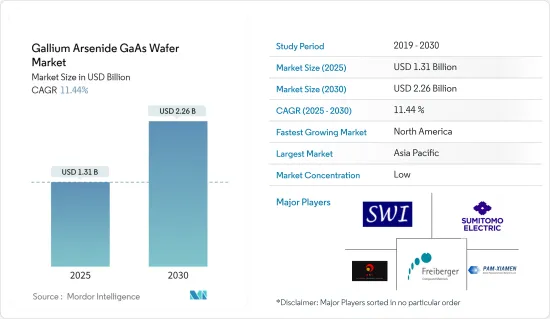
ガリウムヒ素(GaAs)ウエハ市場規模は、2025年に13億1,000万米ドルと推定され、予測期間(2025-2030年)のCAGRは11.44%で、2030年には22億6,000万米ドルに達すると予測されます。
GaAsは主に半導体製造などのエレクトロニクス分野で一般的に使用されています。LED、レーザーダイオード、オプトエレクトロニクスデバイス、モノリシックマイクロ波集積回路などの製品でGaAsウエハの採用が増加していることが、調査対象市場の成長を促進する主な要因の一つと考えられています。この化合物の価格が規制されることで、ガリウムヒ素(GaAs)ウエハメーカーの成長機会が増えます。
ガリウムヒ素またはGaAsは、2つの元素からなる化合物材料です。GaAsウエハの製造に使用される半導体はダイレクトバンドギャップ半導体であり、電子が干渉をあまり受けずにコンポーネントを素早く通過できるため、オプトエレクトロニクスデバイスに特に有用です。
スマートフォンやコンピューティングデバイスの普及が進み、一般照明への発光ダイオード(LED)の普及が進んでいることが、この市場の大きな成長促進要因となっています。また、IoTの登場も市場動向拡大の大きな要因の一つとなっています。この技術は、GaAsベースのICを搭載した高周波通信デバイスの需要も生み出しています。
その結果、複数の通信会社が通信インフラを拡大するにつれて、GaAsウエハの需要は増加し、今後数年間の研究市場の成長にプラスの影響を与えると思われます。さらに、GaAsウエハ固有の特徴により、エレクトロニクス、航空宇宙・防衛、通信など、さまざまなエンドユーザー産業でGaAsウエハのニーズが高まっており、これもGaAsウエハの世界の需要を牽引しています。
例えば、GaAsウエハは、放射線障害に強い広い直接バンドギャップ材料であるため、高出力の宇宙用電子機器や光学窓にも最適であり、市場拡大の好機となるとともに、電子戦システム、電気航空機、ブロードバンド携帯電話ネットワーク技術の開発など、新たな市場動向や使用事例を生み出すと予測されています。
しかし、GaAsウエハの価格は、その利用率の低さを説明する大きな欠点の一つです。このような問題を解決するため、研究者たちは、シリコンに代わるデバイスの製造に役立つ低コストのガリウムヒ素薄膜の新しい製造方法を実現し、調査市場の成長を支えています。
COVID-19パンデミックの世界の発生と、それに続くウイルスの蔓延を抑えるために取られた政府の決定的な行動は、半導体分野に顕著な影響を与え、半導体部品の製造に影響を与え、顧客需要を低下させ、それによって世界市場の成長を阻害しました。しかし、デジタル技術に触れる機会が増えたことで、先進的な民生用電子機器とそれを支えるデジタルインフラの需要が大幅に高まり、調査対象市場の成長にプラスの影響を与えました。
ガリウムヒ素(GaAs)ウエハ市場動向
高周波エレクトロニクスが市場で大きなシェアを占める
GaAs基板で製造される高周波(RF)デバイスは、無線ネットワーク(WLAN)、4G/5G基地局、モバイル通信、衛星通信、Wi-Fi通信などの無線通信アプリケーションで広く使用されています。このような動向の開発は、4Gや5Gサービスをサポートするスマートフォンやその他の携帯端末に必要とされる、次世代、超小型、高性能のRFフロントエンドチップセットの開発における重要なマイルストーンとなります。
また、GaAsウエハの高効率化と低消費電力化も市場参入企業の採用を促し、GaAsウエハ需要にプラスの影響を与えています。光電子デバイスは、以前はコンピュータ周辺機器や短距離光通信に広く使われていました。それでも、拡張現実(AR)、ライダー、顔認識などの新しい用途で高い需要があります。
世界的に、特にインドやブラジルなどの新興諸国ではインターネットの普及率が上昇しており、GaAsウエハの需要を刺激しています。その後、光ファイバーネットワークやバックホール、基地局、無線通信インフラとのWi-Fi接続製品へのニーズが高まり、世界のインターネットの普及を支えています。
さらに、モバイルデータ消費率の伸びとIoTデバイスの広範な採用も、Wi-Fiやその他の無線通信デバイスへの要求を後押ししています。こうした製品や無線通信関連技術の高い成長率が、GaAsウエハの採用を後押ししています。例えば、5G Americaによると、世界のモバイル5G契約数は2023年の190万件から2027年には590万件に増加すると予想されています。
予測期間中、アジア太平洋地域が市場を独占する
アジア太平洋地域では、インテリジェントな民生用電子機器の需要が増加しています。中国、台湾、日本、インドでは、スマートフォン、ウェアラブル端末、コンピュータ、ラップトップなどの先端技術機器に対する需要が急増しており、この地域の市場成長をさらに促進しています。GaAs製品は、シリコンベースのデバイスよりもデータ・トランスミッションと品質が向上するため、接続性が向上し、需要が増加しています。さらに、GaAs製品は高い歩留まり率で大規模に製造できるため、ビジネスの成長も向上しています。インターネットの普及、4Gおよび5Gネットワークの拡大、電子産業も、この地域におけるGaAsウエハ市場の開拓を後押しすると期待されています。
アジア太平洋地域の主な促進要因の1つは、コンピューティングデバイス、スマートフォン、タブレット、ノートパソコンなどの先端技術機器に対する需要の高まりです。トランジスタのようなGaAs製品は、スマートフォンやその他のワイヤレス通信機器に使用できるため、需要の増加はGaAsウエハのニーズを有望な速度で促進しています。
中国は、エレクトロニクス産業の市場を独占している主要国であり、これは、中国における研究市場の開拓を促進している政府の多大な支援によるものです。例えば、中国政府は業界関係者に資金を提供することで、国内技術市場を促進しています。このような動向は、新規参入企業による同国でのプレゼンス拡大を後押ししています。例えば、2023年2月、GaAsウエハ基板などの化合物半導体ウエハ基板メーカーであるAXT社は、北京工場での事業拡大を発表しました。同社は、化合物半導体基板の主要プロバイダーとしての地位をさらに強化するため、原料抽出設備に投資しました。
中国はまた、5Gインフラ開発、その他の民生用電子機器や電動モビリティ・ソリューションの採用においても主要国のひとつです。例えばMIITによると、2022年末までに中国の5G基地局は約231万局に達します。これらの産業の成長とともに、中国における研究市場の成長に有利な見通しが生まれています。
台湾は、ウエハ市場が技術開発の重要な分野の1つであることを目の当たりにしています。その結果、台湾も世界のGaAsウエハ市場で大きなシェアを占めると予想されています。台湾の企業は、特殊な材料やプロセスに対応するため、フロントエンドとバックエンドの先進パッケージング・アーキテクチャのサプライチェーン・ニーズに取り組んでおり、その結果、調査された市場全体に影響を与えています。
ガリウムヒ素(GaAs)ウエハ産業概要
ガリウムヒ素(GaAs)ウエハ市場は競争が激しく、AXT Inc.、住友電気工業、Semiconductor Wafer Inc.、Freiberger Compound Materials GmbH、Xiamen Powerway Advanced Materialなど少数の企業が大きな市場シェアを占めています。既存企業は、研究開発に多額の投資を行い、より優れた技術的に高度な製品を顧客に提供することで、その地位を強化することに注力しています。
2023年5月、半導体ウエハのスペシャリストであるQEは、マイクロLEDディスプレイの認定用に特別に設計された200mm RGBエピタキシャルウエハの新製品群を発表しました。同社によると、GaNとGaAsエピタキシーは、マイクロLEDの急速な普及を促進する上で引き続き重要な役割を果たすと予想されています。
2022年5月、南カリフォルニア大学情報科学研究所のMOSISサービスとWINセミコンダクターズ社は、WINセミコンダクターズ社のGaAsおよびGaNプロセス技術によりGaAsおよびGaNモノリシックマイクロ波集積回路の開発を加速させる覚書に調印しました。このパートナーシップは、MOSISサービスとWINセミコンダクターズとのマルチプロジェクト・ウエハ(MPW)プロジェクトを通じて、信頼性が高く、革新的で、効果的な設計と試作のフローをサポートします。
その他の特典
- エクセル形式の市場予測(ME)シート
- 3ヶ月間のアナリストサポート
目次
第1章 イントロダクション
- 調査の前提条件と市場定義
- 調査範囲
第2章 調査手法
第3章 エグゼクティブサマリー
第4章 市場洞察
- 市場概要
- 業界の魅力度-ポーターのファイブフォース分析
- 供給企業の交渉力
- 買い手の交渉力
- 新規参入業者の脅威
- 代替品の脅威
- 競争企業間の敵対関係
- 技術スナップショット
- 液体封止チョクラルスキー(LEC)成長GaAs
- 垂直勾配凍結(VGF)成長GaAs
- COVID-19の市場への影響評価
第5章 市場力学
- 市場促進要因
- 世界の5Gインフラ採用の増加
- オプトエレクトロニクスデバイスの需要急増
- 市場抑制要因
- 高い製造コスト
第6章 市場セグメンテーション
- 用途別
- 高周波エレクトロニクス
- 発光ダイオード
- 光起電力デバイス
- フォトトニックデバイス
- その他の用途
- 地域別
- 米国
- 台湾
- 中国
- 日本
- 英国
- ドイツ
- 世界のその他の地域
第7章 競合情勢
- 企業プロファイル
- Semiconductor Wafer Inc
- AXT Inc.
- Freiberger Compound Materials GmbH
- Xiamen Powerway Advanced Material Co. Ltd.
- Sumitomo Electric Industries Ltd.
- Wafer Technology Ltd.
- MTI Corporation
- Vital Materials Co Limited
- Dowa Electronics Materials Co. Ltd.
- American Elements
第8章 投資分析
第9章 市場機会と今後の動向
The Gallium Arsenide GaAs Wafer Market size is estimated at USD 1.31 billion in 2025, and is expected to reach USD 2.26 billion by 2030, at a CAGR of 11.44% during the forecast period (2025-2030).
GaAs is mainly used is common in electronics, such as semiconductor manufacturing. The growing adoption of GaAs wafers in products such as LEDs, laser diodes, optoelectronic devices, and monolithic microwave integrated circuits is considered among the primary factors driving the growth of the studied market. The price of this compound being regulated creates more growth opportunities for gallium arsenide (GaAs) wafers manufacturers.
Gallium Arsenide or GaAs is a compound material made up of two elements. The semiconductor used to manufacture GaAs wafers is a direct bandgap semiconductor, meaning that electrons can pass through components much quicker without much interference, making them particularly useful in optoelectronic devices.
The increasing adoption of smartphones and computing devices and the growing penetration of light-emitting diodes (LEDs) in general lighting are significant growth drivers for this market. The advent of IoT has also been one of the major reasons responsible for the increasing market trend. The technology has also created a demand for high-frequency communication devices with GaAs-based ICs.
As a result, with several telecommunication companies expanding their communication infrastructure, the demand for GaAs wafers will increase, which will positively influence the growth of the studied market in the forthcoming years. Additionally, owing to its inherent features, the need for GaAs wafers across various end-user industries such as electronics, aerospace & defense, and communications is increasing, which, in turn, is also driving the demand for GaAs Wafers globally.
For instance, GaAs wafers are also a great choice for high-power outer space electronics and optical windows due to their wide direct bandgap material that resists radiation damage which is also predicted to offer profitable chances for market expansion and give rise to new market trends and use cases, including their higher adoption in electronic warfare systems, electric aircraft, and developments in broadband cellular network technology.
However, the price of GaAs wafers is among the major disadvantage, which explains its low utilization. To solve such issues, researchers have achieved new methods of manufacturing thin films of low-cost gallium arsenide to help create devices that would replace silicon to support the studied market's growth.
The global outbreak of the COVID-19 pandemic and the subsequent decisive government actions taken to curb the spread of the virus had a notable impact on the semiconductor sector, affecting the manufacture of semiconductor components and lowering customer demand, thereby impeding the global market's growth. However, higher exposure to digital technologies significantly enhanced the demand for advanced consumer electronic devices and supporting digital infrastructure, which positively influenced the growth of the studied market.
Gallium Arsenide (GaAs) Wafer Market Trends
Radio Frequency Electronics to Hold the Significant Share in the Market
Radio-frequency (RF) devices produced with GaAs substrates are widely used in wireless communication applications, including wireless networks (WLAN), 4G/5G base stations, mobile communication, satellite, and Wi-Fi communications. The development of such trends marks an important milestone in developing next-generation, ultra-compact, and high-performance RF front-end chipsets that are needed for smartphones and other handsets, supporting 4G and 5G services.
GaAs wafers' higher efficiency and lower power consumption are also enticing market participants to adopt them, positively influencing the demand for GaAs wafers. Optoelectronic devices were previously widely used in computer peripherals and short-range optical communications. Still, they are in high order for new applications such as augmented reality (AR), lidar, and facial recognition.
Globally, internet penetration is rising, especially in developing countries such as India and Brazil, stimulating the demand for GaAs wafers. Subsequently, the need for fiber-optic networks and backhaul, base stations, and Wi-Fi connectivity products with wireless communication infrastructure and have supported the growing penetration of the internet worldwide, which, in turn, is driving the adoption of GaAs wafers.
Further, the growth of mobile data consumption rate and the wide adoption of IoT devices also propel the requirement for Wi-Fi and other wireless communication devices. As a result of the high growth rates for such products and technologies related to wireless communications are aiding the adoption of GaAs wafers. For instance, according to 5G America, the global number of mobile 5G subscriptions is expected to grow from 1.9 million in 2023 to 5.9 million by 2027.
Asia Pacific to Dominate the Market During the Forecast Period
The Asia Pacific region has an increasing demand for intelligent consumer electronic devices. China, Taiwan, Japan, and India have surging demand for advanced technological devices such as smartphones, wearables, computers, and laptops, further augmenting the regional market's growth. GaAs products offer better connectivity through enhanced data transmission and quality than silicon-based devices, so their demand has increased. Additionally, GaAs products can be manufactured on large scales with high yield rates, which improves business growth. The increasing Internet penetration, expansion of 4G and 5G networks, and the electronic industry are also expected to fuel the development of the GaAs wafer market in the region.
One major driving factor in the Asia Pacific region is the growing demand for advanced technological devices such as computing devices, smartphones, tablets, and laptops. As GaAs products such as transistors can be used for smartphones and other wireless communication devices, the growing demand is driving the need for GaAs wafers at a promising rate.
China is the major country dominating the market for the electronics industry owing to considerable government support, which is fostering the development of the studied market in China. For instance, the Chinese government is promoting its domestic technology market by funding the industry players. Such trends are encouraging new players to expand their presence in the country. For instance, in February 2023, AXT, a manufacturer of compound semiconductor wafer substrates such as GaAs wafer substrates, announced an expansion of operations at its Beijing facility. The company invested in raw material extraction facilities to further strengthen its position as the leading provider of compound semiconductor substrates.
China is also among the leading countries in 5G infrastructure development and adopting other consumer electronic and electric mobility solutions. For instance, according to MIIT, by the end of 2022, China had about 2.31 million 5G base stations. Together the growth of these industries is creating a favorable outlook for the growth of the studied market in China.
Taiwan has witnessed the wafer market as one of the critical areas of technological development. As a result, Taiwan is also expected to hold a significant market share in the global GaAs wafer market. Companies across Taiwan are addressing the supply chain needs of front and back-end advanced wafer-level packaging architectures to cater to specialty materials and processes, thus, influencing the overall market studied.
Gallium Arsenide (GaAs) Wafer Industry Overview
The Gallium Arsenide GaAs Wafer Market is competitive and highly concentrated with a few companies such as AXT Inc, Sumitomo Electric Industries Ltd., Semiconductor Wafer Inc, Freiberger Compound Materials GmbH, Xiamen Powerway Advanced Material Co. Ltd, holding a significant market share. Established companies focus on strengthening their position by investing heavily in R&D and providing customers with better and technologically advanced products.
In May 2023, QE, a semiconductor wafer specialist, introduced a new range of 200mm RGB epitaxial wafer products specifically designed for microLED display qualification. According to the company, GaN and GaAs epitaxy is anticipated to continue to play a crucial role in driving the rapid adoption of microLEDs.
In May 2022, The MOSIS Service of Information Sciences Institute, University of Southern California, and WIN Semiconductors Corp. signed a Memorandum of Understanding (MoU) to accelerate the development of GaAs and GaN monolithic microwave integrated circuits with WIN Semiconductors' GaAs and GaN process technologies. The partnership will support the reliable, innovative, and effective design and prototyping flow through the multi-project wafer (MPW) projects with the MOSIS Service and WIN Semiconductors.
Additional Benefits:
- The market estimate (ME) sheet in Excel format
- 3 months of analyst support
TABLE OF CONTENTS
1 INTRODUCTION
- 1.1 Study Assumptions and Market Definition
- 1.2 Scope of the Study
2 RESEARCH METHODOLOGY
3 EXECUTIVE SUMMARY
4 MARKET INSIGHTS
- 4.1 Market Overview
- 4.2 Industry Attractiveness - Porter's Five Forces Analysis
- 4.2.1 Bargaining Power of Suppliers
- 4.2.2 Bargaining Power of Buyers
- 4.2.3 Threat of New Entrants
- 4.2.4 Threat of Substitute Products
- 4.2.5 Intensity of Competitive Rivalry
- 4.3 Technology Snapshot
- 4.3.1 Liquid Encapsulated Czochralski (LEC) Grown GaAs
- 4.3.2 Vertical Gradient Freeze (VGF) Grown GaAs
- 4.4 Assessment of the Impact of COVID-19 on the Market
5 MARKET DYNAMICS
- 5.1 Market Drivers
- 5.1.1 Increasing Adoption of 5G Infrastructure Across the World
- 5.1.2 Surging Demand for Opto-electronic Devices
- 5.2 Market Restraints
- 5.2.1 High Production Cost
6 MARKET SEGMENTATION
- 6.1 By Application
- 6.1.1 Radio Frequency Electronics
- 6.1.2 Light Emitting Diodes
- 6.1.3 Photovoltaic Devices
- 6.1.4 Phototonic Devices
- 6.1.5 Other Applications
- 6.2 By Geography
- 6.2.1 United States
- 6.2.2 Taiwan
- 6.2.3 China
- 6.2.4 Japan
- 6.2.5 United Kingdom
- 6.2.6 Germany
- 6.2.7 Rest of the World
7 COMPETITIVE LANDSCAPE
- 7.1 Company Profiles
- 7.1.1 Semiconductor Wafer Inc
- 7.1.2 AXT Inc.
- 7.1.3 Freiberger Compound Materials GmbH
- 7.1.4 Xiamen Powerway Advanced Material Co. Ltd.
- 7.1.5 Sumitomo Electric Industries Ltd.
- 7.1.6 Wafer Technology Ltd.
- 7.1.7 MTI Corporation
- 7.1.8 Vital Materials Co Limited
- 7.1.9 Dowa Electronics Materials Co. Ltd.
- 7.1.10 American Elements
