ウエハー洗浄装置:市場シェア分析、産業動向、統計、成長予測(2025年~2030年)
Wafer Cleaning Equipment - Market Share Analysis, Industry Trends & Statistics, Growth Forecasts (2025 - 2030)- 発行日
- ページ情報
- 英文 120 Pages
- 納期
- 2~3営業日
- 商品コード
- 1851710
- カスタマイズ可能 お客様のご希望に応じて、既存データの加工や未掲載情報(例:国別セグメント)の追加などの対応が可能です。詳細はお問い合わせください。
- 適宜更新あり 本レポートは最新情報反映のため適宜更新し、内容構成変更を行う場合があります。ご検討の際はお問い合わせください。
- 翻訳ツール提供対象 PDF対応AI翻訳ツールの無料貸し出しサービスのご利用が可能です
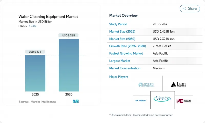
ウエハー洗浄装置市場規模は2025年に64億2,000万米ドル、2030年には93億2,000万米ドルに達すると予測され、2025-2030年のCAGRは7.74%です。
この拡大は、10nm以下のパーティクル除去が必須となる1.6nmプロセス技術への半導体業界の動きを反映しています。EUVリソグラフィーの採用、台湾、韓国、中国、米国における鋳造能力の増強、炭化ケイ素と窒化ガリウムの300mmウェハーへの移行が、ウエハー洗浄装置市場全体の需要を拡大しています。フッ素系温室効果ガスをターゲットとする環境規制と超純水コストの上昇により、装置の選択基準が変化しているが、水効率の高いソリューションや極低温ソリューションを提供するサプライヤーがシェアを獲得しています。洗練されたプロセスノウハウ、長い認定サイクル、サービスのフットプリントが参入障壁となっているため、競合の激しさは依然として緩やかです。
世界のウエハー洗浄装置市場の動向と洞察
3次元NANDとDRAMノードのシュリンクの急増が無欠陥FEOL洗浄の需要を牽引
2030年までに1,000層の3-D NANDを目指す量産ロードマップでは、層が増えるたびにパーティクルによる歩留まり損失が増加するため、洗浄工程が増えます。SK Hynixは、2028年までのメモリ拡張に750億米ドルを計上し、80%を高帯域幅メモリに向ける。ラムリサーチは、深いトレンチでのポリマー残留を軽減するためにCryo 3.0エッチングを導入しました。サブオングストロームの除去精度を実現する装置メーカーは、層数の増加から恩恵を受け、ウエハー洗浄装置市場を引き上げています。メモリー工場は、現在、工具購入の決定を10nm以下の除去効率の実証と契約上結びつけており、長期的な需要を強化しています。
米国、韓国、台湾における鋳造能力の拡大が新たな工具設置基盤を生み出す
CHIPS法は、TSMCのコンプレックスが数千のプロセスツールを必要とするアリゾナでの大規模なツール調達を引き起こしました。サムスンとSKハイニックスは、2047年までに16の新工場に622兆ウォン(約4,710億米ドル)を投じ、当面の受注サイクルを強化しました。東京エレクトロンは、次世代の機会を確保するため、研究開発費を5年間で1兆5,000億円とほぼ倍増させました。生産能力増強は3nm以下に重点を置いており、先進的なウエハー洗浄装置市場参入企業のみが対応可能なツールスペックとなります。工具のリードタイムが短く、サービスに近接していることから、全自動洗浄プラットフォームの注文が直ちに急増しました。
フッ素系温室効果ガス(F-GHG)の厳しい排出規制
世界の半導体業界はPFOAを段階的に廃止することを約束し、化学物質の選択肢が狭まりました。米国環境保護庁(EPA)のPFAS見直し加速は、化学物質のロードマップに不確実性をもたらします。欧州の半導体工場は、主に減衰モジュールの改修により、2010年から2020年にかけてPFC排出量を42%削減しました。装置メーカーは現在、スクラバーとクローズドループの化学リサイクル装置をバンドルしているため、取得コストが上昇し、ROIのタイムラインが延び、ウエハー洗浄装置市場の成長予測が緩やかになっています。
セグメント分析
全自動プラットフォームは、高度なロジックラインにおける厳格なコンタミネーションコントロールの義務化により、2024年の売上高の74.5%を占め、ウエハー洗浄装置市場を自動化優先のパラダイムに置いた。半自動ツールはR&Dクリーンルームに留まり、手動システムは特殊またはレガシーフローに限定されました。全自動化分野は、AIを活用したレシピ最適化により、年率8.5%の成長が見込まれています。当社のスピンスクラバー「SS-3200」は、純水使用量を削減しながら毎時500枚のウエハーを処理し、交換サイクルを下支えしています。
マシンコントローラーに組み込まれたプロセス分析は、現在、ロットごとに数百万のデータポイントを保存し、工場がエクスカーションを予測し、ライン停止を防ぐことを可能にします。ベンダーは、ノズルの汚れや流れの不安定にフラグを立てる予知保全モジュールを組み込んでいます。このようなデジタル・ワークフローは、スマート・マニュファクチャリングに沿ったもので、プレミアム価格をサポートします。その結果、ウエハー洗浄装置市場では、購買決定が設備投資のみから、稼働時間指標と節水を軸とした総所有コストへとシフトしています。
ウエハースプレーラインは、設置面積の小ささ、化学薬品の節約、レシピの柔軟性を兼ね備え、2024年には33.2%の売上シェアを獲得し、ウエハー洗浄装置市場の軌道維持に貢献しました。極低温CO2装置は、新しいものではあるが、液体排出がほぼゼロであることから、CAGRの見通しが最速の12.2%を記録しました。バッチ式浸漬ツールは大量の汎用ラインで生き残り、バッチ式スプレーは中位層を占めました。スクラバーは、化学薬品だけでは対応できないブランケット酸化物の除去に貢献しました。
東京エレクトロンの低温エッチングは、CO2排出量を80%削減し、グリーンケミストリーの主張を実証しました。ACM調査のUltra C Tahoeは、従来の性能に匹敵する一方で硫酸の使用量を75%削減し、複数の鋳造工場で採用されました。現在、技術決定は、パーティクルカウントのスペックと同様に、水と温室効果ガスの指標を中心に行われており、ウエハー洗浄装置市場における枚葉式ウエハーのイノベーションの戦略的重要性が強化されています。
ウエハー洗浄装置市場は、動作モード(自動装置、その他)、技術タイプ(枚葉式スプレー、枚葉式低温、その他)、ウエハーサイズ(<=150 Mm, 200 Mm, 300 Mm, and>=450 Mm)、アプリケーション(スマートフォンおよびタブレット、メモリデバイス、その他)、エンドユーザー(鋳造、IDM、OSAT)、地域(北米、欧州、アジア太平洋、南米、中東アフリカ)で区分されます。
地域分析
アジア太平洋地域は2024年の売上の72.5%を占め、台湾、韓国、中国におけるクラスター投資が、合計で月産770万枚以上の洗浄能力を設置しました。高雄と新竹における鋳造の拡張は、近い将来のツールの普及を促進し、輸出規制下にある中国のIDMの急増は、国内ツールの普及を促進しました。
北米のシェアは、CHIPS法補助金を活用したTSMCアリゾナ工場とインテル・オハイオ工場の投資によって上昇しました。これらの工場は、米国を拠点とするサービスチームとスペアパーツハブを指定し、ウエハー洗浄装置市場内のベンダー選択力学を変化させました。
欧州は専門分野でのリーダーシップを維持した:InfineonとSTMicroelectronicsはSiC生産を拡大し、オランダは1,200万ユーロを投じてChipNLセンターを立ち上げ、洗浄と計測のプラットフォームを共同開発しました。自動車向け需要が堅調な工具更新を支えました。
南米と中東・アフリカでは、組立工場からの需要が漸増しました。アラブ首長国連邦とブラジルの政府による優遇措置は、現地でのウエハー洗浄サービスを必要とするバックエンド施設の誘致を目指しており、ウエハー洗浄装置市場の長期的な地域多様化を示唆しています。
その他の特典:
- エクセル形式の市場予測(ME)シート
- 3ヶ月間のアナリストサポート
よくあるご質問
目次
第1章 イントロダクション
- 調査の前提条件と市場の定義
- 調査範囲
第2章 調査手法
第3章 エグゼクティブサマリー
第4章 市場情勢
- 市場概要
- 市場促進要因
- 3次元NANDとDRAMノードのシュリンクの普及が無欠陥FEOL洗浄の需要を牽引
- 米国、韓国、台湾における鋳造能力の拡大が新たな工具設置ベースを生み出す
- 新しいウエットベンチ化学薬品を必要とする300mm SiCおよびGaNパワーウエハーへの移行
- 超低パーティクルクリーン<10 nmを必要とするEUVリソグラフィの採用
- 米国輸出規制にもかかわらず、中国IDMによる急速なファブ投資
- 市場抑制要因
- フッ素系温室効果ガス(F-GHG)の厳しい排出規制
- 干ばつに見舞われやすい半導体拠点における超純水(UPW)コストの上昇
- BEOLにおける高い設備投資強度と代替ドライプラズマクリーニングの比較
- バリューチェーン分析
- 規制とテクノロジーの展望
- ポーターのファイブフォース分析
- 新規参入業者の脅威
- 買い手の交渉力
- 供給企業の交渉力
- 代替品の脅威
- 競争企業間の敵対関係
- 投資分析
第5章 市場規模と成長予測
- 動作モード別
- 自動機器
- 半自動装置
- 手動機器
- 技術タイプ別
- 枚葉式スプレー
- 枚葉式クライオジェニック
- バッチ浸漬
- バッチスプレー
- スクラバー
- ウエハーサイズ別
- 150 mm以下
- 200 mm
- 300 mm
- 450 mm以上
- 用途別
- スマートフォンおよびタブレット
- メモリーデバイス
- RF機器
- LED
- パワーディスクリートとIC
- CMOSイメージセンサー
- エンドユーザー別
- ファウンドリ
- 統合デバイスメーカー(IDM)
- 半導体組立・テストアウトソーシング(OSAT)
- 地域別
- 北米
- 米国
- カナダ
- メキシコ
- 欧州
- ドイツ
- フランス
- 英国
- 北欧諸国
- その他欧州地域
- アジア太平洋地域
- 中国
- 台湾
- 韓国
- 日本
- インド
- その他アジア太平洋地域
- 南米
- ブラジル
- メキシコ
- アルゼンチン
- その他南米
- 中東・アフリカ
- 中東
- サウジアラビア
- アラブ首長国連邦
- トルコ
- その他中東
- アフリカ
- 南アフリカ
- その他アフリカ
- 北米
第6章 競合情勢
- 市場集中度
- 戦略的動向
- 市場シェア分析
- 企業プロファイル
- SCREEN Semiconductor Solutions Co., Ltd.
- ACM Research Inc.
- MEI Wet Processing Systems & Services LLC
- Modutek Corporation
- Akrion Technologies LLC
- RENA Technologies GmbH
- JST Manufacturing Inc.
- Yield Engineering Systems(YES)Inc.
- AP&S International GmbH
- Semsysco GmbH
- MT Systems Co., Ltd.
- Expertech Systems Inc.
- Samco Inc.
- Naura Technology Group
- Applied Materials
- Tokyo Electron Limited(TEL)
- Kaijo Corporation
- Surpass Industry Co., Ltd.
- Kingsemi Co., Ltd.
- Hwatsing Technology Co., Ltd.
第7章 市場機会と将来の展望
- 発行日
- 発行
- Mordor Intelligence
- ページ情報
- 英文 120 Pages
- 納期
- 2~3営業日


