
|
市場調査レポート
商品コード
1910440
電子設計自動化ツール(EDA):市場シェア分析、業界動向と統計、成長予測(2026年~2031年)Electronic Design Automation Tools (EDA) - Market Share Analysis, Industry Trends & Statistics, Growth Forecasts (2026 - 2031) |
||||||
カスタマイズ可能
適宜更新あり
|
|||||||
| 電子設計自動化ツール(EDA):市場シェア分析、業界動向と統計、成長予測(2026年~2031年) |
|
出版日: 2026年01月12日
発行: Mordor Intelligence
ページ情報: 英文 120 Pages
納期: 2~3営業日
|

概要
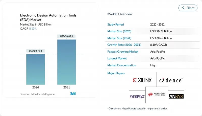
電子設計自動化ツール(EDA)市場規模は、2026年に207億8,000万米ドルと推定され、2025年の192億2,000万米ドルから成長が見込まれます。
2031年の予測では306億7,000万米ドルに達し、2026年から2031年にかけてCAGR8.1%で拡大する見通しです。
この見通しは、トランジスタの微細化加速、AIを活用した設計フロー、ファウンドリと設計ツールの連携強化に基づいています。チップ設計者は、手動によるルール調整からデータ駆動型最適化へ移行しており、これによりテープアウトサイクルの短縮とリスピンのリスク低減が図られています。クラウドベースのキャパシティバーストにより高度な検証技術へのアクセスが拡大する一方、自動車分野の機能安全規制が形式手法を主流設計へ押し進めています。2025年に完了予定のシノプシスによるアンシス社350億米ドル買収は、シリコン・パッケージ・システム全体の性能を同時に最適化できる統合デバイス・システムプラットフォームへの体系的な移行を示しています。一方、地政学的な輸出規制は並行するEDAエコシステムを促進し、ベンダーは収益減少を回避するため複数地域のファウンドリ向けにフローの認証を迫られています。
世界の電子設計自動化ツール(EDA)市場の動向と洞察
先進ノードにおけるチップ密度の急増
ゲート・オール・アラウンド(GAA)トランジスタ、裏面給電技術、マルチダイパッケージングにより、設計ルールチェック(DRC)は7nmプロセスと比較して10倍に増加しています。ファウンドリは現在、EDAリーダー企業と共同でフローを開発しており、シノプシスとTSMCは2025年4月にA16およびN2Pノード向けの完全なデジタル・アナログツールチェーンの認証を完了しました。統一された探索からサインオフまでの環境は、コストのかかる再設計を削減します。3nmプロセスでは、再設計のコストは1件あたり5,000万米ドルを超えます。インテルの18Aプログラムも同様に、単一の基板上に演算、メモリ、I/Oを統合する2.5D/3Dアーキテクチャ向けの統合フローに依存しています。
AI/MLアクセラレータとカスタムSoCの普及
ハイパースケールおよびエッジプロバイダーは、専用推論シリコンの採用を加速しています。カデンツ社は2025年第1四半期に半導体IP収益が前年比40%増を記録し、この成長はAIおよびチップレットプロジェクトに起因すると説明しています。NVIDIA、ASML、TSMC、シノプシス各社は、CuLithoソフトウェアスタックによるリソグラフィシミュレーション速度の40倍高速化を達成し、AIの電力効率目標を満たすレチクルレイアウトを実現しました。アクセラレータの異種混在化が進む中、SIPの再利用やパッケージ内相互接続規格の標準化がIP検証の需要を加速させております。
主要EDAスイートのライセンシングコスト上昇
包括的な3nmサインオフのための年間エンタープライズバンドルは、現在1シートあたり100万米ドルを超え、中堅ファブはツールモジュールの優先順位付けと更新サイクルの延長を余儀なくされています。寡占的な供給構造により、特にオープンソース代替品が存在しないタイミングクロージャーやリソグラフィシミュレーションパッケージにおいて、ベンダー側の価格決定力が維持されています。
セグメント分析
半導体知的財産(SIP)は、検証済みインターフェースブロックや混合信号コアを必要とするチップレットアーキテクチャの増加により、ツールカテゴリー中最も高い9.7%のCAGR予測を示しています。2025年にはSIPが電子設計自動化ツール(EDA)市場収益の18.74%を占めましたが、ファウンドリが既知良品ダイ戦略を推進する中、プロジェクト当たりのアタッチレートは2023年比で倍増しています。SIPアプリケーション向け電子設計自動化ツール(EDA)市場規模は、モノリシックSoCからヘテロジニアスアセンブリへの移行を背景に、2031年までに大幅な成長が見込まれます。
IC物理設計・検証分野は、配置配線・静的タイミング・DRCが全テープアウト工程で必須であることから35.82%のシェアを維持しています。ただしAI強化フロアプランニングによる多目的最適化の自動化により、最近の3nm設計ではターンアラウンドタイムが30%短縮されました。
フロントエンド設計ツールは、高レベル合成(HLS)や自然言語からRTLへの生成ツールによる生産性向上により、CAGR 9.35%を記録しています。RTL自動化分野における電子設計自動化ツール(EDA)市場規模は、機能意図を少ない反復で捕捉するAI支援コード生成技術の後押しを受け、2031年までに大幅な成長が見込まれます。レイアウト・配線・タイミングクロージャーは依然として電子設計自動化ツール(EDA)市場シェアの32.10%を占めており、サインオフレベルのタイミング収束と高度な3D寄生成分抽出の代替不可能性を反映しています。
ジェネレーティブ設計プラットフォームは現在、配置ガイダンスを生成し、人的スクリプトと比較して配線長を11%、リーク電流を9%削減します。しかしながら、最終的なSOC引き渡しには、鋳造が承認する認定済みタイミングおよび電気的ルールレポートが依然として必要であり、確立されたバックエンドツールチェーンの重要性が確固たるものとなっています。
電子設計自動化ツール(EDA)レポートは、ツールタイプ(コンピュータ支援設計、IC物理設計・検証など)、設計フロー段階(フロントエンド設計RTLなど)、導入形態(オンプレミス、クラウドベースなど)、エンドユーザー業界(通信インフラ、民生用電子機器など)、地域(北米など)別に分類されています。市場予測は金額(米ドル)で提供されます。
地域別分析
アジア太平洋地域は2025年に42.05%のシェアを占め、2031年までCAGR9.55%で拡大します。台湾と韓国におけるファウンドリ集積が地域のツール需要を支える一方、中国は米国の輸出規制に対応し、自国開発のEDAスタック構築を加速させています。政府主導の施策により、AI支援配置配線エンジンやSPICEシミュレータへの補助金が投入され、3nmプロセス量産化前にフローの現地化を目指しています。インドは豊富なエンジニア人材を活かし、欧米顧客がコスト効率の高いRTL・DFT支援を求める中、現地設計サービス企業は2024年に17%成長しました。
北米はAIアルゴリズム、IPカタログ、クラウドインフラにおける主導権を通じて影響力を維持しています。同地域のシェアは2025年に29.15%へ小幅に縮小したもの、最先端ノード向けリファレンスツールフローの主要供給源であり続けています。輸出管理体制によりベンダーはライセンスキーのジオフェンシング実装を義務付けられており、コンプライアンスコストが増加する一方で北米のIPチェーンが固定化されています。インテルファウンドリーとシノプシスの18A認定フローにおける協業は、米国が先進製造シェア回復を目指す動きを強化しています。欧州は自動車・産業用途に注力し、ISO 26262規格がプレミアム検証ツールの導入を促進しています。TSMCが2025年にミュンヘンに設計センターを開設する目的は、ファウンドリ技術者を地域サプライチェーンに組み込み、3D-ICパッケージングや省電力型AIアクセラレータに対する直接的な支援を提供することにあります。EUチップ法による助成金は、電子設計クラスター向けの研究開発税額控除を重点的に支援し、地域のEDA導入をさらに促進します。中東・アフリカおよび南米は依然として発展途上ですが、政府主導のファブプロジェクトやIoT展開が進む地域では二桁成長を示しています。
その他の特典:
- エクセル形式の市場予測(ME)シート
- アナリストによる3ヶ月間のサポート
よくあるご質問
目次
第1章 イントロダクション
- 調査の前提条件と市場の定義
- 調査範囲
第2章 調査手法
第3章 エグゼクティブサマリー
第4章 市場情勢
- 市場概要
- 市場促進要因
- 先進ノードにおけるチップ密度の急上昇
- AI/機械学習アクセラレータおよびカスタムSoCの普及
- クラウドネイティブEDAワークフローの台頭(EDA-as-a-Service)
- 自動車業界におけるISO 26262機能安全規格の適合要件
- オープンソースハードウェアの広がりが検証需要を牽引
- 米国と中国の輸出管理の二極化が加速する国内設計フロー
- 市場抑制要因
- 主要EDAスイートのライセンシング費用の高騰
- 5nm以下の物理設計エンジニアの人材不足
- クラウド導入における知的財産権侵害およびサイバー侵入リスク
- 予想を下回るムーアの法則の延長ペース
- バリューチェーン分析
- 規制情勢
- テクノロジーの展望
- ポーターのファイブフォース分析
- 供給企業の交渉力
- 買い手の交渉力
- 新規参入業者の脅威
- 代替品の脅威
- 競争企業間の敵対関係
- 投資分析
- マクロ経済要因が市場に与える影響
第5章 市場規模と成長予測
- ツールタイプ別
- コンピュータ支援エンジニアリング(CAE)
- IC物理設計および検証
- プリント基板(PCB)およびマルチチップモジュール(MCM)
- 半導体知的財産(SIP)
- サービス
- 設計フロー段階別
- フロントエンド設計(RTL)
- 論理合成および機能検証
- レイアウト、配線、タイミングクロージャ
- 最終承認(DFM、電源、SI、熱設計)
- 展開モード別
- オンプレミス
- クラウドベース
- エンドユーザー産業別
- 通信インフラ
- 民生用電子機器
- 自動車・モビリティ
- 産業・エネルギー
- 航空宇宙・防衛
- 医療機器
- その他の産業
- 地域別
- 北米
- 米国
- カナダ
- メキシコ
- 南米
- ブラジル
- アルゼンチン
- その他南米
- 欧州
- ドイツ
- 英国
- フランス
- イタリア
- その他欧州地域
- アジア太平洋地域
- 中国
- 日本
- 韓国
- インド
- その他アジア太平洋地域
- 中東
- サウジアラビア
- アラブ首長国連邦
- その他中東
- アフリカ
- 南アフリカ
- その他アフリカ
- 北米
第6章 競合情勢
- 市場集中度
- 戦略的動向
- 市場シェア分析
- 企業プロファイル
- Ansys Inc.
- Cadence Design Systems Inc.
- Synopsys Inc.
- Siemens Digital Industries Software(Mentor Graphics)
- Keysight Technologies Inc.
- Altium Limited
- Zuken Ltd.
- Xilinx Inc.(AMD Adaptive and Embedded Computing Group)
- Aldec Inc.
- Agnisys Inc.
- Lauterbach GmbH
- Silvaco Inc.
- Real Intent Inc.
- Axiomise Ltd.
- Imperas Software Ltd.
- PDF Solutions Inc.
- Flex Logix Technologies Inc.
- Andes Technology Corp.
- Cobham Gaisler AB
- Arteris Inc.

